Quantcast
Channel: Power management
Viewing all 437 articles
Browse latest View live

How to design a limited power source industrial AC/DC power supply with minimal components – part 2

$
0
0


Part one of this blog discussed basic needs of a Limited Power Source (LPS) and provided a brief overview of standards that govern LPS circuits.

To address the needs of protection and limiting, conventional power supplies as illustrated in Figure 1 rely on multiple feedback loops based on two or more optocouplers. These optocouplers transmit the load voltage, load current and open-fault information to the main controller – typically a flyback controller for wattages up to 150W. In addition, the current-sensing circuitry has external current-sense resistors, precision operational amplifiers for amplification and setting the constant current-constant voltage (CC-CV), and constant power feedback loops. Overall, discrete circuits have high component counts, use up valuable real estate on the board and add cost to the system.

Figure 1: Typical block diagram showing the conventional architecture of a 100W industrial power supply

Figure 2 shows a proposed design architecture with reduced feedback loops. The architecture uses the UCC28740, a CC-CV flyback controller with optocoupled feedback for voltage and primary-side regulation (PSR) for constant current. The high level of integration of the controls in the UCC28740 controller aids in low component count design and reduced cost.

Figure 2: Proposed design architecture with reduced feedback loops

The two key benefits of this proposed architecture are:

  • Precise current and power limit, just with primary-side sensing. In the conventional approach shown in Figure 1,The output load current is sensed through discrete operational amplifier circuits and transmitted to main controller through opto-coupler. In some cases an additional opto-coupler is used for feedback redundancy. the output load current is directly sensed and the information is fed back to the flyback controller through a separate optocoupler circuit. The proposed architecture, on the other hand, uses cost-effective and reliable primary-side current sensing. A high degree of precision in the output-current limit is made possible by precision PSR current-sense techniques embedded into the UCC28740. The current limit causes the voltage foldback and ensures tight power limiting.
  • Cost-effective open-loop protection and feedback redundancy. The conventional approach shown in Figure 1 uses two feedback loops, both of which are based on optocouplers. The identical nature of these optocouplers and their associated circuitry bring in an additional risk of failure; each of the optocouplers can fail simultaneously under similar stress conditions, which can be detrimental.

The proposed architecture uses a single optocoupler feedback precision-output voltage control. A PSR circuit provides a redundant voltage-control loop. PSR activates during open-loop conditions such as failure in the optocoupler feedback network. Thus, output voltage is limited and regulated  to the value set by as  the primary-side feedback components.

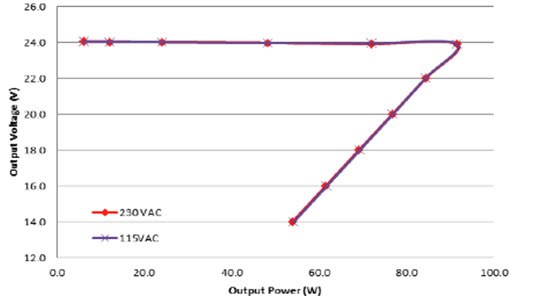
The  60W, 24V High Efficiency Industrial Power Supply with Precision Voltage, Current and Power Limit highlights the performance results of precision current and voltage limiting. Figures 3 and 4 show the results of the reference design board for precision current regulation and power foldback.

Figure 3: Precision CC-CV operation


Figure 4: Precision power foldback characteristics

 Additional resources

Explore these industrial power-supply reference designs:

References

IEC60950-1 Information Technology Equipment - Safety - Part 1: General Requirements

NFPA 70: National Electrical Code (NEC) standard


Output inductor considerations in a synchronous buck converter

$
0
0

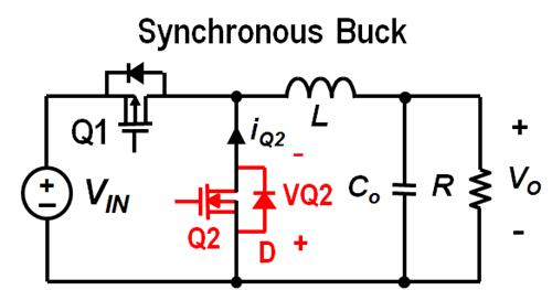
Inductors are an essential component of switching voltage regulators and synchronous buck converters, as shown in Figure 1. In all switching regulators, the output inductor stores energy from the power input source when the MOSFETs switch on and releases the energy to the load (output).

Figure 1: Synchronous buck DC/DC converter

You should select inductors to manage output capacitor size, load transients and output ripple current. There are benefits of both low and high inductance values.

The benefits of low inductance include:

  • Lower DC resistance (DCR), which is inherent in the inductor wire, and which affects ripple and power loss.
  • Higher saturation current, for higher output-current capability.
  • Higher slew rate (di/dt), which improves load transient response and reduces output capacitance for a given load transient.

The benefits of high inductance include:

  • Lower ripple current, which in turn reduces:
    • AC losses (inductor skin effect).
    • MOSFET root-mean-square (RMS) current.
    • Output capacitor RMS current.
    • Output capacitance for an equivalent output ripple.
    • Continuous inductor current over a wider load range.

Equation 1 calculates the output inductor value:

where L is the output inductance, VOUT is the target output voltage, VIN(max) is the maximum input voltage, FS is the buck converter switching frequency and IRIPPLE is the target output ripple current.

I recommend sizing the ripple current for 10% to 30% of full load. Plugging values into Equation 1, Equation 2 shows the output inductance calculation result:

In this case, I selected the PG0077.801 inductor from Pulse Electronics. Table 1 shows its relevant parameters.

Table 1: PG0077.801 inductor parameters (image courtesy of Pulse Electronics)

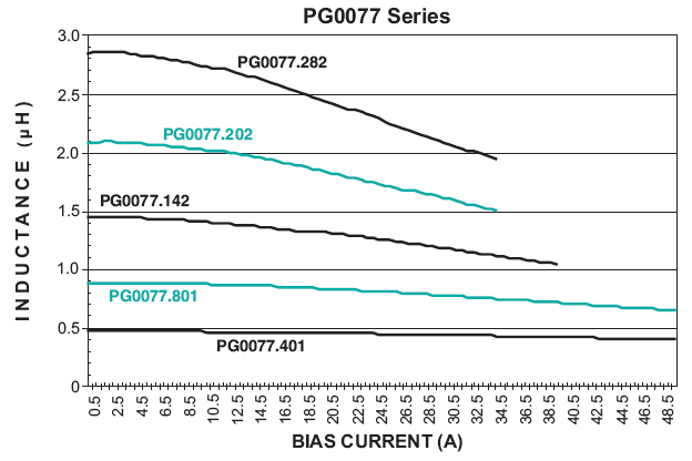
It is important to check the inductance vs. the load (bias) current, as inductance decreases with increasing current. Then you can determine what the actual inductance is at the target load current.

If you assume 15A of continuous output current, the actual inductance is 0.83mH, as shown in Figure 2.

Figure 2: Inductance vs. current (image courtesy of Pulse Electronics)

Once you know the actual inductance value, you can recalculate the ripple and RMS currents. Equation 3 recalculates ripple current:

Equation 4 recalculates RMS current:

You can also calculate the inductor losses. Total inductor losses are winding losses and core losses, expressed by Equations 5 and 6:

where K1 = 13.77 x 10⁻⁹ , K2 = 39.4, FSW = 500kHz, DI = 3.32A (the calculated ripple current) and PCORE = 0.983W.

In this example, the total inductor power loss is 0.294W + 0.983W = 1.277W.

There are many inductor types to choose from, but most buck DC/DC converters typically use ferrite drum and iron powder toroid inductors. So when designing a buck converter, keep these inductor selection criteria in mind for a high-performance, stable and reliable design. Check out TI’s buck converter and buck controller selection tables for a variety of buck DC/DC solutions.

How an eFuse can help provide robust industrial power path protection

$
0
0

Any electronic systems are often subjected to harsh environments and threats such as electrostatic discharge (ESD), electrical fast transient (EFT) and lightning surges. Power designers must prioritize circuit protection to prevent system failure, especially for industrial applications with a 24V supply rail. 

Circuit protection schemes are capable of protecting the power supply and the overall system from events such as overcurrent, short circuit, input inrush current, overvoltage, undervoltage, input reverse polarity protection (commonly known as miswiring) and reverse current blocking.

In this blog I will give an overview of several approaches to robust industrial power path protection including discrete implementation, hot-swap plus ORing controller approach and integrated implementation.

Discrete implementation

Figure 1: Discrete protection scheme

Discrete implementation schemes are the most traditional way of power path protection using a protection scheme in the power path one example is shown in Figure 1.

A discrete implementation utlizes a power diode in series to protect the system from reverse polarity (miswiring) and reverse current. If a circuit draws 2A of current, it dissipates ~1W of power across the diode, which will increase the board temperature. Resonant circuit (L-C) filters and multiple TVS diodes control the input line transients during surge test (International Electrotechnical Commission (IEC) 61000-4-5).

The implementation utilizes a PFET (high-side switch) along with bi-polar junction transistor BJTs, operational amplifiers, Zener diodes, resistors and capacitors to fulfill all protection requirements. This system solution is bulky and has a larger bill of materials (BOM) count. Additionally, this implementation does not address thermal shutdown protection and current-limit accuracy variations with temperature.

By utilizing a traditional fuse, a discrete implementation protects against short-circuit events. The fuse takes milliseconds to seconds to break during short circuit, which can damage the load. Be sure to check out my colleague’s blog for more information on upgrading your fuse.

Hot-swap plus ORing controller approach

Figure 2: Controller + MOSFET protection scheme

Another common approach, as shown in Figure 2, to power protection is through a hot-swap controller and an ORing controller. This scheme uses external FETs to make the design more efficient and reliable. Unfortunately, this implementation still has challenges, such as controlling external FETs, external sense resistance and implementing an additional circuit for input reverse-polarity protection. This implementation struggles to manage thermal and safe operating area (SOA) protections due to the external FET architecture. Even though this solution is better than a discrete implementation, it is not suitable for space-constrained systems such as input/output (I/O) modules.

Integrated implementation (eFuse)

Figure 3: Integrated protection scheme

On the other hand, imagine that your entire discrete implementation vanishes into a single integrated device, barring a few components like Transient Voltage Suppressor (TVS) diodes, resistors and capacitors, as shown in Figure 3. That would be really cool, right? An eFuse typically integrates all of the protection features mentioned above into single device, efficiently and with minimal design efforts.  EFuses also incorporate features like voltage, current monitoring and fault indication for system diagnosis – apart from power path protection.

The SOA protection of FETs and robust thermal protection ensures the protection of the eFuse, as well as the load in harsh environments. It is also suitable for space-constrained applications, as integration helps reduce the system solution by more than half.

One of these types of solutions is the TPS2660, the industry’s first 60V back-to-back FET integrated eFuse. The device is definitely worth considering for your new designs as it supports protection against inrush current, overcurrent, short circuit, input reverse polarity protection (miswiring), overvoltage and undervoltage conditions. It also provides current monitoring and fault indication for system diagnosis. The integrated 60V back-to back-FET architecture lets you design robust circuits and protect loads against industry-standard tests such as surge (IEC 61000-4-5), EFT (IEC 61000-4-4), and voltage dips and interruption tests in accordance with IEC 61131-2.

A robust and efficient power supply protection scheme is essential for electronic system design.  With integrated protection devices, designers can create their system more simply, , efficiently and get to market faster. If you have a design which uses power path protection for 24V power supply rail, stay a step ahead and start designing today with the Input Protection and Backup Supply Reference Design for a 25W PLC Controller Unit.


Additional resources

How to meet power sequencing requirements with a PMIC

$
0
0

When designing a power solution for an application processor, your first considerations are often the number of rails needed, the output voltage and the maximum load current. There are tools like the Quick Search that can help you select the right power-management IC (PMIC) for the processor or application, whether it’s an industrial application like Factory Automation or Human Machine Interface (HMI), or an automotive application like infotainment or advanced drivers assistance systems (ADAS).

But you also need to ask yourself:

  • How will you handle power-up and power-down sequencing?
  • How will you ensure the completion of the power-down sequence when power is removed?

Let’s take a look at these questions in more detail.

Power-up and power-down sequencing

Power-up and power-down sequencing are very important and are specified in the processor’s data manual. If the PMIC has enable pins and voltage-selection pins for each rail, one idea for handling power-up and power-down sequencing would be to have each PMIC output enable the next regulator in the sequence. This has a few drawbacks, however, since the output voltage needs to be high enough to send a logic-high signal to the enable, and it also makes a reverse power-down sequence very difficult, if not impossible.

A second approach is to use a microcontroller’s general-purpose input/output (GPIO) pins to enable each rail in sequence to meet the sequencing requirements. However, this requires extra pins (and therefore a bigger package), as well as a sequencing microcontroller and some firmware to get the system running.

An easier way is to use the PMIC’s one-time programmable (OTP) memory, which contains default output voltages and power-up and power-down sequencing for the device. So when the PMIC is enabled or disabled, a pre-programmed sequence will execute without any interaction from a microcontroller. The PMIC can also start the power sequence within a few milliseconds, which leads to faster boot times than when booting up a microcontroller before running power sequencing.

Using the PMIC in different configurations doesn’t require any different firmware, or actually any firmware at all. For example, the TPS659037 has two different configurations, based on the orderable part number, to power the AM572x Sitara™ depending on processor frequency and the number of cores used. The PMIC will enable or disable core rails depending on the configuration. So you can use the same PMIC in two different configurations, with no hardware changes or additional firmware development.  Configurations for other processors or applications are possible by programming a different sequence in the OTP memory.

Power-down sequence when power is removed unexpectedly

There is often more to the power-down sequence than just meeting the timing requirements. Even though the PMIC contains a power-down sequence that meets the processor’s timing requirements, what happens when power is removed unexpectedly? If the input voltage to the PMIC is removed very quickly, there won’t be enough input power to maintain the output voltage during sequencing. In a simple solution, all rails will discharge based on output capacitance and load current. It may not be easy to predict the ramp-down rates, so it’s possible that the power-off could happen out of order. So how do you fix this?

You need a way to block reverse current, a method to store energy and a disable signal to the PMIC. A Schottky diode can block reverse current when the input is removed. Capacitors can hold up the input voltage while the power-down sequence occurs. Disabling the PMIC will depend on the system configuration, however. In many cases, it is desirable to have an always-on system, so let’s consider a case in which the system will be enabled when power is first supplied. You can create an always-on system in one of two ways:

  • A supervisor, which creates a logic signal to indicate that power is good, for systems where VIN directly powers the PMIC.
  • A power-good signal for systems using a pre-regulator to generate the PMIC supply.

Figure 1 shows the implementation of the first option, while Figure 2 shows the implementation of the second option.

Figure 1: Supporting uncontrolled power down when VIN powers the PMIC


Figure 2: Supporting uncontrolled power down when a pre-regulator powers the PMIC

In the case of the pre-regulator, the pre-regulator output capacitance can also act as the energy storage to hold VCC up. You should base your chosen total supply capacitance on the worst-case leakage current during power down so that the voltage is held up until the power-down sequence completes.

Use Equation 1 to calculate the required capacitance:

Where I is the leakage current, Vcc is the supply voltage to the PMIC, Vmin is the minimum input voltage the PMIC needs to operate, and ΔT is the time it takes the power-down sequence to complete. For TI’s TPS659037 and TPS65916, Vmin is 2.75V, and the pre-programmed power-down sequence is typically 1ms.

See our PMIC page to learn about more ways to enable your system power with TI’s broad portfolio of scalable PMICs.

Additional resources


Don’t power your FPGA like this!

$
0
0


Oops. I attached my field-programmable gate array (FPGA) to the output of my DC/DC converter and now the DC/DC won’t start. When I look at the circuit with an oscilloscope, I see Figure 1. The output voltage just doesn’t enter regulation. What went wrong?

Figure 1: Because of this FPGA’s high startup load and very high decoupling capacitance, the DC/DC converter cannot bring its output voltage into regulation

FPGAs present some unique challenges for their power supplies. For example, FPGA vendors typically require hundreds or even thousands of microfarads (µF) of decoupling capacitance on their input supply to maintain the required regulation of the FPGA’s supply voltage among the different frequencies of transients produced by the FPGA, as well as to reduce ripple on the supply voltage. Many FPGAs also require a specific startup time (not too fast and not too slow) and startup monotonicity (with VOUT reaching its set point in a straight line without any downward movements).

In addition to FPGA-related design challenges, more and more FPGA designers must also design the power supply for their FPGA. Being FPGA experts, many of these designers have little experience in power-supply design and so need a very simple power supply – a power module is an obvious choice.

Power modules achieve simplicity by integrating many or all of the required passive components. Fewer components to select results in a faster and simpler design time. Control-loop compensation is one of the first things to integrate into the power module, but this constrains the design’s stable range – and with the large amount of capacitance, an internally compensated power module may not be stable. Consult the device data sheet and application notes for guidance on stability. The DCS-Control topology used in many of TI’s TPS82xxx power modules is very stable and supports a wide range of output capacitance.

The very small size of power modules means there are fewer pins to work with. Fewer pins means a simpler device, but also fewer features. Another feature commonly integrated into power modules is soft-start (SS) time. This time is set internally on some power modules, like the TPS82085, but is programmable with a capacitor on other power modules, like the TPS82130. A programmable SS time is generally required for meeting a specific startup time requirement and is very helpful for starting a power module with all of that capacitance connected.

But let’s get back to what went wrong. In the waveform shown in Figure 1, the DC/DC converter can’t start up when driving the FPGA and its capacitance. This application note explains the details, but here is a short summary of various ways to fix the issue:

How have you overcome startup issues in your past designs?


Additional resources:

Power Tips: Improve power supply reliability with high voltage GaN devices

$
0
0

Gallium nitride (GaN) high electron mobility transistors (HEMT) improve converter efficiency, with a lower gate charge, lower output charge and lower on-resistance then silicon FETs with the same voltage rating. In high-voltage DC/DC converter applications with bus voltages greater than 380V, depletion-mode (d-mode) GaN HEMTs are more popular than enhancement-mode (e-mode) GaN HEMTs. That’s because d-mode GaN HEMTs have a much wider gate voltage range than e-mode GaN HEMTs. However, d-mode GaN HEMTs have a “normally on” feature, which is not desirable for common switch-mode power-supply applications. Two commercially available high-voltage GaN devices, shown in Figure 1, use d-mode GaN HEMTs with different configurations to form “normally off” devices.

Figure 1: High-voltage GaN devices using synchronous drive technology (a); and direct drive technology (b)

Both GaN devices have a high-voltage GaN HEMT in series with a low-voltage silicon FET but have different driving schemes. A high-voltage GaN device with synchronous-drive technology shorts its high-voltage GaN HEMT gate pin to the source pin of its low-voltage silicon FET. By switching the low-voltage silicon FET on, you can control the on/off of the whole device.

There are three possible states of a synchronous-drive high-voltage GaN device:

  • Forward blocking. When VDS,device> 0 and VGS,LV_Si< VGS(th),LV_Si, the high-voltage GaN HEMT could be either on or off, depending on whether VDS,device is higher than the high-voltage GaN HEMT VGS threshold voltage (VGS(th),HV_GaN). Notice VGS(th),LV_Si is the VGS threshold voltage of the low-voltage silicon FET. Since VGS,LV_Si< VGS(th),LV_Si, the low-voltage silicon FET is in an off state without conducting any current. If VDS,device< |VGS(th),HV_GaN|, the high-voltage GaN HEMT maintains the on state and the low-voltage silicon FET holds the VDS stress of the entire device. If VDS,device≥ |VGS(th),HV_GaN|, the high-voltage GaN HEMT turns off and the VDS voltage of the high-voltage GaN HEMT maintains at VDS,device + VGS(th),HV_GaN, where VGS(th),HV_GaN< 0.
  • Forward conduction. When VDS,device> 0 and VGS,LV_SiVGS(th),LV_Si, the low-voltage silicon FET is on. Regardless of whether the high-voltage GaN HEMT is off or on before entering the forward conduction state, the conduction of the low-voltage silicon FET will force VGS,HV_GaN≈ 0 and turn on the high-voltage GaN HEMT.
  • Reverse conduction. When VDS,device< 0 and VGS,LV_Si< VGS(th),LV_Si, VGS,HV_GaN will clamp to the low-voltage silicon FET body-diode forward voltage. Therefore, current will flow through the low-voltage silicon FET body diode and the high-voltage GaN HEMT. When VDS,device< 0 and VGS,LV_SiVGS(th),LV_Si, the low-voltage silicon FET then turns on and VGS,HV_GaN is forced to zero. Therefore, current flows through the drain-source channel of both the low-voltage silicon FET and high-voltage GaN HEMT.

Unlike synchronous-drive high-voltage GaN devices, a direct-drive high-voltage GaN device only switches the low-voltage silicon FET on once after its VDD voltage goes above undervoltage lockout. You can analyze device operation under these two conditions:

  • Without VDD applied. When VDD is not yet applied to the device after applying a positive VDS,device, VGS,HV_GaN stays at a zero voltage and the VDS of the low-voltage silicon FET starts to increase. When the VDS voltage increases to VGS(th),HV_GaN, the high-voltage GaN HEMT will turn off and hold the voltage of VDS,device+VGS(th),HV_GaN. This operation is similar to the forward-blocking state of a synchronous-drive high-voltage GaN device.
  • With VDD applied. After the device powers up by applying VDD, the gate driver can generate a negative voltage to turn off the high-voltage GaN HEMT directly. Once the gate driver takes control of the high-voltage GaN HEMT, the low-voltage silicon FET can then be on continuously before removing VDD or detecting any failure.

With a different driving technology, synchronous-drive high-voltage GaN devices and direct-drive high-voltage GaN devices have very different features. Synchronous-drive high-voltage GaN devices can be used as a drop-in replacement for silicon FETs. However, the low-voltage silicon FET is synchronously switched with the high-voltage GaN HEMT. That is, the body diode of the low-voltage FET may conduct current in a steady-state operation. Therefore, the low-voltage silicon FET reverse-recovery charge (Qrr) will introduce additional losses and limit the achievable switching frequency with a synchronous-drive high-voltage GaN device.

In contrast to a synchronous-drive high-voltage GaN device, the low-voltage silicon FET in a direct-drive high-voltage GaN device only switches from off to on once and stays on in steady state. This eliminates the reverse-recovery effect due to the low-voltage silicon FET body diode. In addition, the integration of gate driver and startup logic increases the reliability of whole power supply.

TI’s 600V LMG3410 GaN device adapts direct-drive technology to achieve zero Qrr and lower gate charge. Overtemperature protection (OTP) and overcurrent protection (OCP) with a 50nS fast-fault trigger time are also built in. Using TI direct-drive GaN devices in power supplies with a totem-pole switch configuration – like a totem-pole power-factor correction circuit or an inductor-inductor-capacitor (LLC) series resonant half-bridge converter – can eliminate the worry of shoot-through and improper dead-time setting.

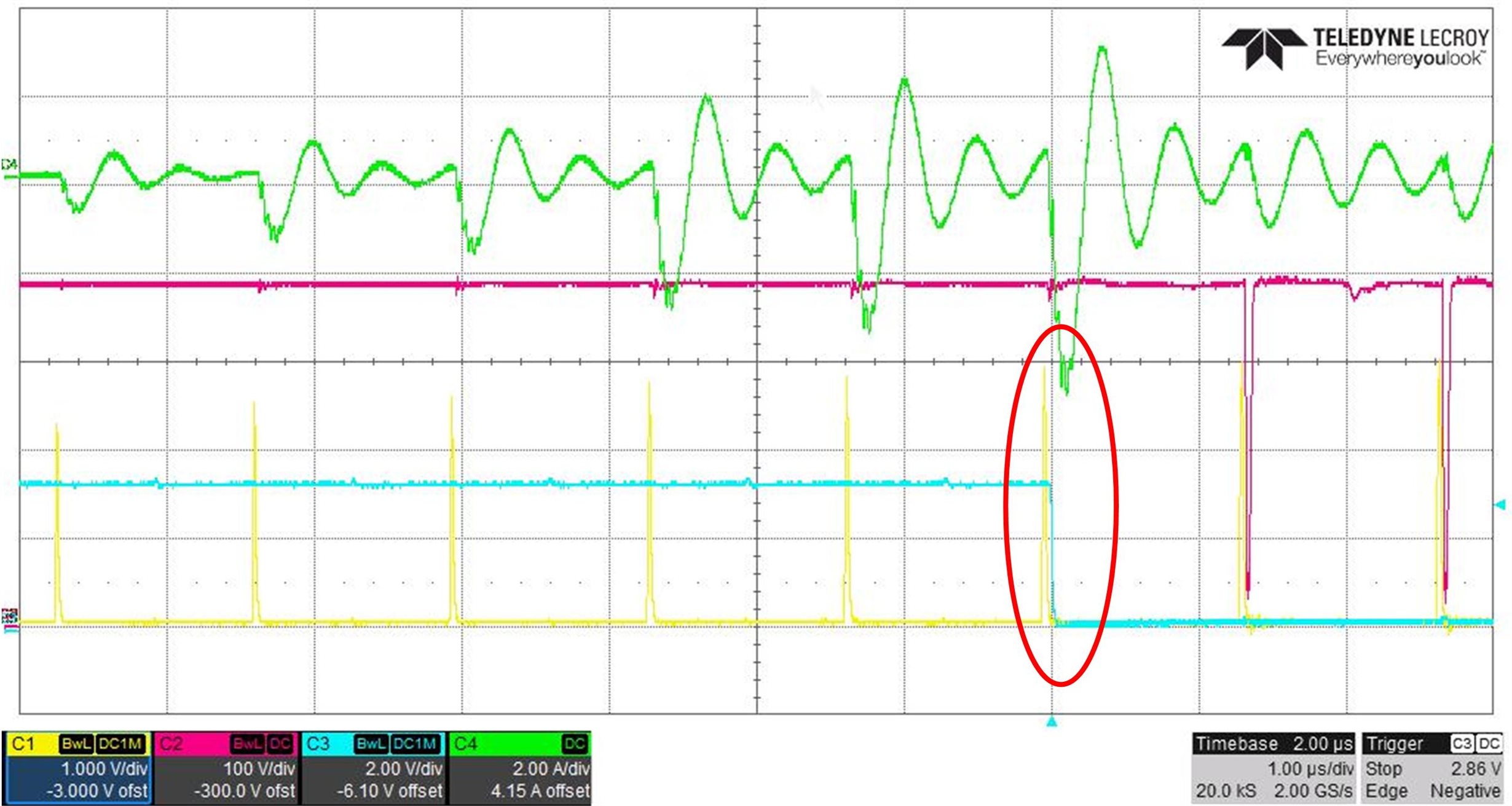
Figure 2 shows a shoot-through test on an LLC series resonant half-bridge converter with the TI LMG3410 as input switches. During the test, a high-side switch is forced on, with the low-side switch controlled by a driving signal with gradually increased duty cycles. Once the OCP trips, the LMG3410 quickly disables its driver inside to turn off the switch. This prevents the device from catastrophic failure.

Figure 2: An TI LMG3410 shoot-through test on an LLC series resonant half-bridge converter: C1 = low-side switch driving signal, CH2 = switching-node voltage, CH3 = high-side switch driving signal, CH4 = primary inductor current

We also tested LMG3410 OTP on the same LLC series resonant half-bridge board with an improper dead-time setting to force the converter into hard-switching operation. You can watch the OTP testing video.

With OCP and OTP built into this zero Qrr GaN device, you’ve cleared the most worrisome issues of totem-pole switches. Contact your local TI representative to get a LMG3410 daughtercard to evaluate how TI direct-drive GaN devices improve system reliability and efficiency.

Additional resources


PMBus benefits in multi-rail systems

$
0
0

You can find hardware systems with multiple low-voltage rails that need regulation, sequencing and monitoring in cloud infrastructure equipment like base stations, networking switches, servers and storage, as well as test and measurement applications such as integrated circuit (IC) testers, oscilloscopes and network analyzers.

The Power Management Bus (PMBus) digital interface is a popular interface, which I discussed in another blog post, “A PMBus primer: common PMBus questions answered.”

TI has a complete PMBus power solution for systems using 48VDC on the front end and 12VDC or another low-voltage DC rail as the intermediate bus; see Figure 1.

Figure 1: 48V to point-of-load PMBus power system

The benefits of a complete PMBus solution in multirail systems are many: ease of use; reduced design time (as a new design can be generated in seconds by reconfiguring the on-chip nonvolatile memory [NVM]); reduction in overall component count and total solution cost; a unified and seamless design and programming method through a single graphical user interface (GUI); much simpler board characterization through PMBus margining; and improved diagnostics through voltage, current, temperature, power and fault monitoring.

Multirail PMBus sequencers/managers such as the 24-rail UCD90240 and the new 32-rail UCD90320 can sequence, margin, monitor and report faults for up to 32 rails using TI’s Fusion Digital Power™ GUI. They can also be stacked in fours for up to 128 rails, managed through the SYNC_CLK pin if needed.

Additionally, the UCD90240 and UCD90320 have true black-box logging that provides detailed information about all rails, General Purpose Input (GPI), and General Purpose Output (GPO) status on the first fault, as shown in Figure 2.

Figure 2: UCD90240/UCD90320 black-box logging

UCD90xxx PMBus sequencers/managers work with analog and PMBus point-of-load voltage regulators to provide a PMBus management and voltage-regulation solution in multirail systems, which almost always have one or more high-current application-specific integrated circuits (ASICs), processors and/or field-programmable gate arrays (FPGAs).

The loads require precise multiphase step-down conversion from the 12V intermediate bus to their respective rails. Typical load currents range from 50A to 200A, and the multiphase converter may require up to six phases to distribute power and thermals effectively and reduce the size and count of the inductor and output capacitors through phase interleaving.

One such six-phase converter is the TPS53667.

How does a multirail UCD90xxx PMBus sequencer come together with multiple PMBus voltage regulators in a design? The TI Designs PMBus Power System for Enterprise Ethernet Switches Reference Design is a good example, as shown in Figure 3.

The design employs a PMBus sequencer, a PMBus hot-swap IC (for the input current) and eight analog and PMBus voltage regulators, including a four-phase PMBus buck controller and a double-data-rate (DDR) termination (Vtt) switcher. The Fusion Digital Power GUI provides a graphical representation of the power tree and offers the capability to program the main parameters on the top half, while monitoring key parameters such as voltage, current, temperature and power on the bottom half.

Figure 3: The reference design’s PMBus board and Fusion Digital Power GUI

If you are designing multirail systems with high-current processors, ASICs and/or FPGAs and want to simplify your design and characterization, reduce development time, and increase your system’s diagnostic capability, consider TI’s PMBus power solutions.

Additional resources

How to simplify high-voltage power-supply design

$
0
0

High voltage power supplies are ubiquitous whether you are designing an AC/DC adapter or your high voltage on-board power supply for industrial applications. You find them commonly to step down your high voltage input voltage to a lower intermediate voltage before you power your point-of-load (POL) converters. The design of these front-end power supplies pose unique challenges from the requirements that they have. This post is intended to give you a basic understanding of high-voltage power-supply design, and how design tools can make it simple to design for these applications. There are three main things that you need while designing for your AC/DC or high-voltage DC/DC application.

1. Understand your system requirements.

Most of you know where your end equipment will be used and whether you will need a universal voltage range (85V to 265V) or region-specific voltages such as U.S. (120V), Japan (100V), U.K. (230V) or China (220V). Also, are you designing for a charger-type application or an on-board power supply? Are you designing for a supply that needs tight output-voltage regulation? What type of isolation requirements do you have?

The answers to each of these questions will help you make appropriate trade-offs while you design. Designing for universal voltage ranges ensures operability across different parts of the globe at the expense of higher voltage-/current-rated components, which come at a higher price and footprint. Charger-type supplies typically require a constant-voltage/constant-current (CV/CC) characteristic. So selecting a controller that meets this requirement is essential.

If your power supply requires tight regulation of the output, you need to consider secondary-side regulated controllers that tightly regulate the voltage on the secondary, versus primary-side controller regulators where the output could vary with changes in the transformer or secondary diode parameters. Certain applications require that your transformer provide a certain class of isolation for safer, robust end equipment.

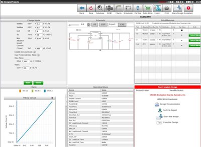
TI’s WEBENCH® High-Voltage Power Designer is an easy to use tool to design your AC/DC or HV-DC/DC applications.  You simply enter your voltage and current requirements and find solutions that work for your application. With the optimizer dial, you can optimize your design for cost, footprint and efficiency based on your system needs. To get started, visit the WEBENCH panel on ti.com. Figure 1 below shows a view of the power solutions generated by WEBENCH Power Designer.

Figure 1: WEBENCH Power Designer with High Voltage solutions

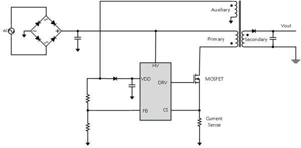
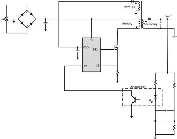
Figure 2 below shows an AC/DC flyback using primary-side regulation that provides a low-cost, low-footprint solution, as well as loose regulation of the output on the secondary. Figure 2 shows an AC/DC flyback in secondary-side regulation using optocoupler feedback, which is more expensive but provides tighter regulation on the secondary.

Figure 2: AC/DC Flyback with primary-side regulation


Figure 3: AC/DC Flyback with secondary-side regulation using optocoupler feedback

2. Select the right topology/control scheme.

At low power (greater than 10W and less than 100W), flyback is the most widely used topology. Forward and half-bridge topologies typically serve power levels from 100W to 500W, with full-bridge topologies serving >500W. Theoretically, you could build a flyback for high power levels too, but the voltage/current stress on the components makes this topology require higher voltage-/current-rated components, which are expensive and bulky. This paves the way for the natural adoption of other topologies at higher power levels.

You could design the controller to operate in continuous conduction mode (CCM) (the magnetizing current in the transformer does not reach zero), discontinuous conduction mode (DCM) (the magnetizing current reaches zero and stays zero till the next switching cycle), or transition mode (TM) (the magnetizing current reaches zero and the next switching cycle starts immediately). CCM is typical for higher power levels, while DCM and TM provide lower-loss solutions.

WEBENCH Power Designer saves you time and effort by creating the complete design for the topology using the necessary equations depending on the device and its operating mode. The tool also lets you evaluate efficiency and also other parameters such as output ripple, the RMS currents, losses etc. at various operating points within the design range.

3. Design your transformer.

One of the main things required in a good high-voltage power supply design is designing the transformer correctly for your applications. The transformer is generally the energy-conversion element in a high-voltage design, which also provides isolation between the primary and secondary.

By definition, transformers do not store energy, but transfer energy from the primary to the secondary. This is one of the main reasons why people refer to flyback transformers as coupled inductors, because components in the flyback topology store energy during the on-time of the switching cycle and then transfer that energy to the secondary during the off-time.

Transformers typically have a core (which is the magnetic element); the bobbin (or coil former), which is the plastic housing for the core (see Figure 4); and the wire that gets wound on the core-bobbin structure.

Figure 4: Core, coil former and assembled transformer

Assembled pre-built transformers are readily available from manufacturers with a fixed turns ratio (Ns/Np) and primary inductance (the magnetizing inductance of the transformer that causes energy to build up). Depending on the operating frequency and output power levels, the requirements for the primary inductance and the turns ratio vary widely, and a pre-assembled off-the-shelf transformer might not be available. In such cases, selecting a transformer core and bobbin and winding the transformer will be necessary. This requires an in-depth knowledge of transformer magnetics.

WEBENCH design tools now give you the ability to design the transformer by selecting the core and bobbin that meet the requirements and also provides the winding structure details as well. You can click on the transformer symbol in the schematic to view and download the transformer details and also to change the transformer core/bobbin combination. Figure 5 shows a view of the transformer design window giving you the various core/bobbin combinations for a specific design requirement. You can also compare different transformers in terms of height, losses (core/copper losses), footprint and cost. If you have a preference for a specific core type or material, use the transformer listing to pick the one that is appropriate for your needs.

The transformer construction diagram gives you instructions on how to wind the transformer. This along with the transformer construction details table gives you information on the number of layers, strands, the AWG of the wire and more. You can also download the transformer design report as shown in Figure 6 to get this information. This will simplify your effort to build the transformer whether you are prototyping it yourself or having it wound by a transformer winding company. 

Figure 5: Transformer design capability in WEBENCH


Figure 6: Transformer Design Report

Additional resources


Extend the input-voltage range of boost controllers

$
0
0

I was recently reading an amusing article posted on The Telegraph titled “50 technological advances your children will laugh at.” It is incredible to see how quickly technology is changing, and how must-have gadgets from one decade become the big, clunky gadgets that kids start laughing at the next decade.

With the increasing number of electronics being powered off of lithium-ion (Li-ion) batteries, it is important to design an efficient and robust power supply. Just take a look around you: I am sure you have at least two or three electronic devices that are being powered off of a battery source. I recently got a new laptop computer and I am impressed with the sleek, compact design that still provides excellent battery life. However, you have to keep in mind that Li-ion batteries will constantly charge and discharge, which will affect the operation of other integrated circuits within the system.

Wide input voltage range DC/DC controllers usually have built-in undervoltage lockout (UVLO) circuits to prevent the converters from misoperating when the input voltage is below the UVLO threshold. In the event of a load transient or a supercapacitor discharging, the input voltage may drop below the UVLO threshold, causing an undesirable shutdown of the system. Furthermore, these controllers generally cannot be used in applications where the input voltage is always lower than the UVLO threshold. You can consider a split-rail approach to extend the boost converter’s input voltage range, however, enabling the use of these controllers in applications where the input voltage is lower than the UVLO threshold.

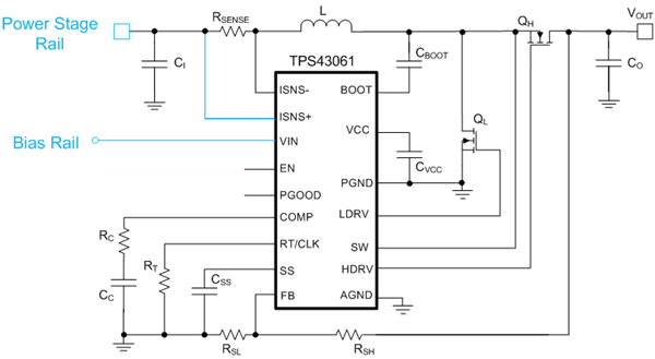
Texas Instruments’ TPS43060 and TPS43061 low quiescent current synchronous boost DC/DC controllers with wide input voltage ranges are used commonly across 5V, 12V and 24VDC bus power systems. Synchronous rectification and a compact 3mm-by-3mm 16-pin solution enable high efficiency and high power density for high-current applications. The TPS43061 is an example of a boost controller that can support a split-rail configuration. As shown in Figure 1, the input supply to the boost converter can split into two rails: the power-stage input rail and the controller’s bias input rail. The power-stage rail is the input to the boost converter for power conversion. The bias input rail is used to power the controller itself, which can be an additional auxiliary supply or derived from the output. With the split-rail configuration, the TPS43061 can support an input as low as 1.9V.

Figure 1: Split-rail configuration

In some applications with only one input supply, the input supply voltage may be greater than the UVLO turn-on threshold at startup but may fall below the range afterwards, causing an undesirable shutdown. One example is a power system using a photovoltaic panel combined with a supercapacitor as an input supply; the input voltage may drop below the UVLO threshold due to the discharging capacitor. For this type of application, if the output voltage is within the bias input specification range (or, in other words, if VOUT is greater than the UVLO turn-on threshold), then VOUT can be fed back as the bias supply through a diode, as shown in Figure 2.

Figure 2: VIN biased from VOUT of TPS43061

With Li-ion batteries used across several applications such as smartphones, tablets and laptop computers, the voltage of a single-cell Li-ion battery can range from 2.7V to 4.2V due to discharge and charge. For these applications, you need a separate bias supply other than the battery input. As shown in Figure 3, a 4.5V or higher source connected to the bias rail can power on the controller. Since the bias supply needs to supply low voltage, you can connect another supply rail within the system above the UVLO turn-on threshold to the bias rail. Another approach is to add a charge pump that can produce the bias voltage.

Figure 3: VIN biased from an additional supply

A split-rail approach separates the power rail from the bias supply rail to eliminate the constraint on the minimum operating voltage of the power rail. By extending the input voltage range of the boost controller, you’ll have more time to design the next must-have gadget. Consider TI’s TPS43060 and TPS43061 low quiescent current synchronous boost DC/DC controllers for your next split-rail design.

Power designs require powerful tools

$
0
0

Your boss just asked you to create a voltage regulator design to power the latest board revision. Do you have all the tools you need to create your design?

  • Brain, check.
  • Books, check.
  • Coffee, check.
  • Tools, hmmm ... maybe …

You probably know the steps you have to take, and of course, you have Google to search for anything not covered in your books or that you might have forgotten about power design (or face it, maybe never knew). You probably have a tool to create your circuit schematic, and you either have a calculator or your computer to calculate the equations. You might even have a SPICE simulator to dive deeper into transient behaviors.

OK, now you’re depressed … am I right? It looks like mountains of work with hurdles to jump, and a headache from the review of multiple datasheets, intense simulation model search and CAD tool updates to ensure it is all compatible, but it’s not.

On top of tool-related struggles, there are the typical power design challenges. You have to carefully consider selecting the right inductors, FETs, diodes and capacitors that will maintain the essential stability requirements and still achieve the necessary efficiency, all while meeting cost and size and heat constraints. You must make trade-offs. But how do you know that you are making good choices and getting the job done quickly without turning it into a research project? Your boss is waiting ...

Well, it doesn’t have to be a struggle. Powerful tools are at your fingertips on TI.com. WEBENCH® Power Designer can do the calculations, select components, make the trade-offs, create the schematic and run simulations in a few minutes and you won’t break a sweat. This tool takes you from a few specifications to a complete design, including a schematic and board layout with the full library included.

Figure 1: WEBENCH® Power Designer

Never heard of it? Worried it might be too difficult? You can learn about all the steps in detail by watching the “Learn WEBENCH Power Designer” video series.

Additional resources

Simplifying 100V wide VIN power conversion

$
0
0

A switching regulator is an efficient device when you need to perform step-down power conversion. The wide input-voltage (VIN) space (which TI considers >30V) has seen an increased usage for these products due to new applications.

Figure 1 shows major applications with wide VIN, along with their nominal bus operating voltage ranges and the transient range that the DC/DC converter will see. Within these applications, the emergence of 48V batteries for automotive and high-cell battery applications such as e-bikes, GPS trackers and drones translates into a growing need for wide VIN up to 48V. The >48V space requires that DC/DC converters withstand transients as high as 100V caused by things like load dump, lightning strike and back-electromotive force from motors, while still regulating 12V and 5V outputs.

Figure 1: Operating voltage ranges by application

Designers traditionally dealt with these transients by putting clamping circuitry on the front end so that the converter doesn’t see the spike. Figure 2 shows an automotive system example where the front-end circuitry adds over a dozen components to the design. All of these components add up as additional cost and space. Also, as the voltages get higher, the ratings of critical components such as diodes and capacitors increase as well, which exponentially increases cost.

TI’s lineup of wide VIN DC/DC Fly-Buck™ converters, which operate up to 100VDC, avoid these issues.

Figure 2: Clamping circuit for an automotive system

Figure 3 shows TI’s wide VIN constant on-time (COT) buck converter portfolio. Not only do these converters eliminate the clamping circuit, but the COT architecture further simplifies designs because it requires no compensation and can maintain high step-down ratios, eliminating intermediate rails. The nonsynchronous LM5007 and LM5009 have been popular in e-meters and power tools, while a lower-current synchronous device such as the LM5017, LM5018, and LM5019 is popular in the servo drive space.

You can configure TI’s LM5017, LM5018, and LM5019 synchronous converters for isolated bias supplies, making the parts optimal for amplifier bias, insulated gate bipolar transistor (IGBT) bias and communication bias such as RS-485. The advantage here is that the Fly-Buck™ topology doesn’t require any secondary feedback circuits such as optocouplers and transformer auxilary windings.

To address the higher-current needs of 100V converters (with motor drives and GPS trackers), the LM5161 has a 100V input voltage range and 1A current range. It is also TI’s first 100V regulator with AECQ-100 qualification, making it useful in 48V automotive applications.

Traditionally, the 100V devices were developed to be used in telecom applications, but are now seeing use cases in automotive and multi-cell battery applications. While the 48V automotive and high-cell battery space is still emerging, like every technology trend, the power density is bound to increase as the applications mature. It will then be much more challenging to incorporate a clamping circuitry on the front end due to size constraints and the high voltage converters with higher current capabilities like the LM5161 will find more use cases. Read the white paper, “Valuing Wide VIN, Low EMI Synchronous Buck Circuits for Cost-Driven, Demanding Applications” for more information on this topic.

Additional resources:

How to simulate a load switch circuit with varying input voltages and loads

$
0
0

Load switches are used in a wide variety of applications, from cars to phones to servers to medical devices, so it would make sense that not everyone uses their load switch the same way. The data sheet will show the performance and specifications, but it can’t capture every application. Perhaps the data sheet shows performance with an input voltage of 1.2V or 1.8V, but your application operates at 1.35V. What should you do? To know what to expect for your specific application, try using TI’s WEBENCH® tool.

Opening a load-switch design in WEBENCH

To start your design, go to the Power Designer Enabled Devices link in TI’s WEBENCH Design Center.  From the list across the top, select the Load Switch option (see Figure 1). By clicking the Create button, the WEBENCH tool will open the product folder for the load switch you selected.

Figure 1: Load-switch WEBENCH device listing

Load switches with WEBENCH capabilities will have the WEBENCH widget on the right side of the product folder. Figure 2 shows the widget for the TPS22965 load switch.

Figure 2: Load-switch widget from the TPS22965 product folder

Using this widget, some of the design parameters are already entered into the tool. The left side of the widget shows the parameter names, the middle is for user entry and the right shows the range of values applicable for that specific load switch. Clicking the Open Design button starts the WEBENCH tool. The display will be similar to the one shown in Figure 3.

Figure 3: WEBENCH Designer layout

Change inputs

At the top-left corner is the Change Inputs section, as shown in Figure 4.

Figure 4: WEBENCH Designer Change Inputs section

After creating a design, the Change Inputs section allows you to go back and modify the design parameters. There are also additional options and parameters depending on the selected load switch. By changing these values, the simulated design results – schematic, graphs and operating values – are updated.

Schematic

By clicking the Schematic box, the schematic for the design will open.

Figure 5: Schematic for the created WEBENCH design

This schematic shows what the design looks like based on the design parameters entered and the load switch configuration. By using this view, you can verify the connections and components used with the load switch.

Operating values

The Operating Values section provides many calculated values that show how the device is expected to perform, taking into account all entered design parameters. Figure 6 shows an example of this section.

Figure 6: WEBENCH Designer Operating Values section

This is one of the most useful sections of the WEBENCH Designer tool, since it tells you what load-switch performance to expect for a very specific application. In-rush current, rise time, efficiency, on-resistance, and power dissipation are just a few of the results calculated. To change these values, simply enter new design parameters in the Change Inputs section. In doing so, you can see how changing the design parameters will change the load-switch behavior. For example, changing the output capacitance will affect the in-rush current for the load switch.

Adding load switches in Power Architect

Your application may have a specific start up sequence due to the different power rails of a processor or FPGA. When designing a power supply using the WEBENCH Power Architect tool, load switches can be added for power sequencing. For instructions on how to do this, please visit the WEBENCH help center.

Unique designs can lead to innovation and success in the marketplace. If you have a design that uses a load switch in a way not specified in the data sheet, use the WEBENCH tool to model the performance and stay a step ahead!

As always, if you need additional support with your design, feel free to post your question on our TI E2E™ Community Load Switches and Power Path Protection forum.

Additional resources


How to achieve higher system efficiency with high-current gate drivers

$
0
0

We live in a world where designers are on a seemingly constant pursuit for higher efficiency. We want more power out with less power in! Higher system efficiency is a team effort that includes (but is not limited to) better-performing gate drivers, controllers and new wide-bandgap technologies.

Specifically, high-current gate drivers can help facilitate overall higher system efficiency by minimizing switching losses. Switching losses occur when a FET switches or turns on and off. To turn a FET on, the gate capacitance must be charged beyond the threshold voltage. The drive current of a gate driver facilitates the charging of the gate capacitance. The higher the drive-current capability, the faster the capacitance can charge or discharge. Being able to source and sink a large amount of charge minimizes power losses and distortion. (Conduction loss is the other type of switching loss in FETs. Conduction losses are defined by the internal resistance, or RDS(on), of the FET where . The FET dissipates power as current is conducted through.)

In other words, the goal is to minimize the switching transition time period in systems that require high-frequency power conversion. The gate-driver specification that highlights this type of performance is the combined rise and fall time. See Figure 1.

Figure 1: Typical rise and fall time diagram

If you want to take it up a notch, gate-driver features like delay matching can effectively double the drive-current capability. Delay matching is the matching of internal propagation delays between two channels. This is achieved by paralleling the outputs, or tying the channels together, of dual-channel gate drivers. For example, TI’s UCC27524A has extremely accurate 1ns (typical) delay matching, which can increase the drive current from 5A to 10A.

Figure 2 shows the UCC27524A’s A and B channels combined into one driver. The INA and INB inputs are connected together, as are OUTA and OUTB. One signal controls the paralleled combination.

Figure 2: The UCC27524A with paralleled outputs to double drive-current capability

One result of increased system efficiency is an increase in power density. The need for higher power densities is a trend in applications like power factor correction (PFC) and synchronous rectification blocks of isolated power supplies, DC/DC bricks and solar inverters, where designers are constrained to the same size (or smaller!) for the same amount of output power.

TI’s portfolio includes gate drivers with high current, fast rise and fall times, and delay matching. See Table 1.

Category

Device

Description

Rise/fall time

Delay matching


High-current drivers


UCC27714

4A, 600V high- and low-side driver

15ns, 15ns

Yes

UCC27524A

5A, high-speed low-side dual driver

7ns, 6ns

Yes

UCC27211A

4A, 120V high- and low-side driver

7.2ns, 5.5ns

Yes

Table 1: High-current gate drivers

Get started on your high-efficiency system today. For more info, see www.ti.com/gate drivers.

Additional resources

How to implement remote sense in your processor power design

$
0
0

Hardware engineers often don’t consider the placement of the sense connection of buck converters in a power-management integrated circuit (PMIC) when powering an application processor. You might be thinking, “The sense pin for a buck converter must be connected to the output. What is there to consider?” Well, many application processors use voltage scaling to minimize the supply voltage in order to reduce power consumption and junction temperature. Minimizing the supply voltage requires a tight voltage tolerance in order to provide the lowest possible supply voltage, and one such voltage tolerance to consider is the I*R drop of the supply current through the printed circuit board PCB trace.

For example, a 2-inch long trace up to 1-inch wide with 0.5oz copper on an evaluation board has about 8mΩ resistance. With a max load of 5A, there could be a drop of as much as 40mV from the PMIC output to the processor input. AM57xx processors provide a target voltage in 10mV steps, which is much smaller than this 40mV variation. So how do you improve this?

Any PCB trace must have resistance, so you can’t remove the I*R drop. But one solution is to route the buck sense pin to the load instead of to the buck output capacitor. If the PMIC is regulating to 1.2V, it will regulate the output voltage so that 1.2V is seen at the load regardless of the load current. A good place to route the sense connection is to one of the bulk capacitors, getting as close as possible to the processor supply pin.

Figure 1 shows an example layout using remote sensing on the buck using the example numbers above. The trace resistance is about 8mΩ and the load current is 5A, giving a 40mV drop from the PMIC output to the processor supply pins. Because the sense voltage is routed to the processor, the PMIC is regulating its target 1.18V at the load, as seen by the red color on the feedback line in Figure 1.

Figure 1: PMIC power trace and remote sense connection (red). The voltage gradient goes from blue (higher voltage) to red (lower voltage)

When routing the sense pin across the board, you need to shield it from noise. Make sure to route the sense line away from other switching lines on the board. I also recommend shielding the sense lines with power or ground planes above and below. If the regulator has differential sensing – meaning that it has a sense output and a sense ground line – route the two lines in parallel in order to reduce common-mode noise. Figure 2 shows an example of differential feedback routing using the TPS659037 regulator SMPS12.

Figure 2: Differential routing feedback showing output voltage feedback (red), ground feedback (orange) and package outline (white)

Sense pin routing is only one aspect of layout guidelines for a PMIC. For more layout guidelines, see the layout section of the device data sheet. Also check out TI’s PMIC selection for more ways to power your application processor.

Additional resources


Input and output capacitor considerations in a synchronous buck converter

$
0
0

Capacitors are an essential component of a synchronous buck converter. There’s a variety of capacitor technologies so it’s important to know what parameter of the input and output capacitors you need to consider when designing a synchronous buck converter as shown in Fig.1.

Figure 1: Synchronous Buck DC/DC Converter


Power capacitors selection considerations are shown in the table 1 below:

Table 1: Buck Converter performance vs. Capacitor Parameter

Table 2 below shows the relative capacitor characteristics depending on the technology.

Table 2: Relative Capacitor Characteristics

Capacitor impedance over frequency is also important as it determines the buck converter switching frequency at which the capacitor acts as a capacitor for energy storage, and not as an inductor.  Impedance can be due to the ESR (Effective Series Resistance) and ESL (Effective Series Inductance) of a capacitor and it looks like a U-shaped curve as shown in Fig.2. The Self-Resonant Frequency, also shown in Fig.2, is the frequency after which the capacitor starts to look like an inductor (example shown for the 10uF capacitor). Ideally, we want the buck converter to switch at a switching frequency in the capacitor region. 

We can use combinations of capacitors to “flatten” the impedance curve with the objective to push the buck converter switching frequency higher while still operating in the capacitive region. Capacitor impedance varies by technology and switching frequency.

 Figure 2: Capacitor Impedance over Switching Frequency

 So, how do you choose a capacitor for an input and output filter?

For an input filter you choose a capacitor to handle the input AC current (ripple) and input voltage ripple.

For an output filter you choose a capacitor to handle the load transients and to minimize the output voltage ripple.

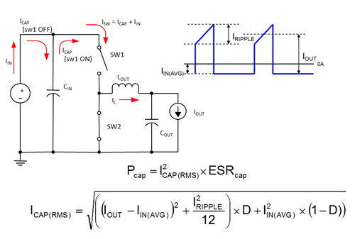
The equation in Fig.3 shows the equation to determine the input current RMS (Root-Mean-Squared) current the capacitor can handle. Based on the input voltage, the input current RMS current, and the input voltage peak-to-peak ripple you can choose the capacitor looking at the capacitor datasheets. It is recommended to use a combination of Aluminum Electrolytic (AlEl) and ceramic capacitors. Ceramic capacitors have low ESR and they can reduce the input voltage peak-to-peak ripple, which, in turn, reduces the input ripple current for the input bulk capacitors to handle.

Figure 3: Input Capacitor RMS Current calculation

When considering output capacitors, table 3 below shows the selection criteria:

Table 3: Output Capacitor Criteria

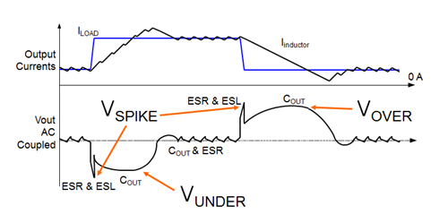
 Fig.4 below shows how each Output Capacitor Component can affect the buck converter load transient performance.

Figure 4: Capacitor criteria in load transient performance

Capacitor calculations for the output voltage overshoot, undershoot, and peak-to-peak voltage ripple are used to determine the capacitance as shown in Figures 5-6 below.

Figure 5: Determining output capacitance for output voltage undershoot and overshoot


Figure 6: Determining output capacitance for output voltage peak-to-peak ripple handling

An example for selecting an output capacitor is shown below:

Output Capacitor Selection Example: 

  • 2A to 10A load step @ 15A/ms
  • Use 2x 1000 mF Aluminum. Elco: 19mW ESR
    • PLOSS = (3.32/2)2 x 19/2 x 10-3 = 0.024W]
  • To help reduce spikes, add two 10 mF ceramics (1210), 0.8mW ESR , 1.1nH ESL each
  • This selection yields:
    • 1.7mV output voltage undershoot
    • 10.7mV output voltage overshoot
    • 19.9mV voltage  spikes
    • 2.8mV of output voltage peak-to-peak ripple

So, when designing a buck converter keep these capacitor selection criteria in mind for a high-performance, stable and reliable design!Consider one of TI’s buck converters and buck controllers for your next DC/DC power supply design. 


How to determine bandwidth from the transient-response measurement

$
0
0

I’ve often thought there must be an easy way to relate the bandwidth of a power-supply control loop to its transient response, but never really found a good reference that defined this in simple terms. It seems like a straightforward problem, which should have a simple solution. The higher the bandwidth, the faster the loop responds, and with less voltage deviation.

Several limiting factors may get in the way of this simple relationship. First is the series resistance of the output capacitor. If the resistance is too high, then the load step creates a large voltage deviation before the control loop can respond. Equation 1 gives the peak voltage deviation:

Second, the inductor can cause slew-rate limiting. This is related to the control-loop bandwidth by the voltage across the inductor, calculated with Equation 2:

Third, there is a critical inductance limit beyond which the duty cycle will saturate. The peak transient voltage is then determined by the large-signal limiting of the inductor current into the output capacitor. This is related to the voltage across the inductor, output capacitor and series resistance, expressed by Equation 3:

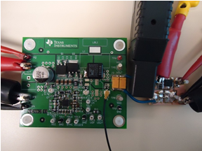
Let’s say you design your power supply to avoid these issues and use an electronic load to test the transient response. If your control-loop bandwidth is relatively high, you may find that the output voltage follows the load current and is not limited by the control loop. In this case, you can use a MOSFET and load resistor on a small board for the load step, controlled by a function generator. A low duty cycle for the load on-time will minimize dissipation in the resistor. It is important to mount this as close to the power-supply output as possible in order to minimize wiring inductance. Figure 1 shows a typical setup. The small black wire connects to a surface-mount coax for the output voltage measurement.

Figure 1: Typical power-supply test setup for fast load transient

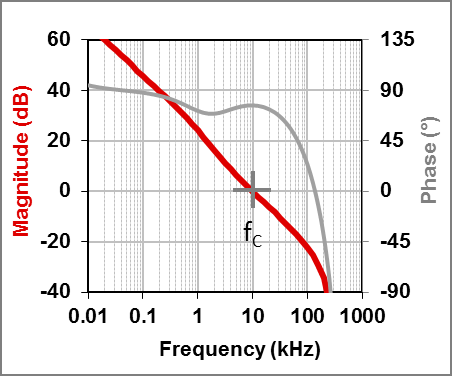
Figure 2 shows the measured transient response, which is directly related to the bandwidth of the control loop in Figure 3. With no equivalent series resistance (ESR), slew rate or duty-cycle limiting, the initial response time is one-fourth the effective control-loop period. This is the equivalent first quarter of a sinusoidal response at the unity-gain frequency. The peak voltage will vary based on the topology and damping, but is easily predictable with a surprising degree of accuracy.

Figure 2: The measured transient response shows tP = 25μs and VP = 130mV for a load step of ∆I = 5A


Figure 3: The corresponding control-loop bandwidth is 10kHz

With no ESR, slew rate or duty-cycle limiting, Equation 4 calculates tP as:

For current-mode control, Equation 5 gives the single-pole approximation that results in the peak voltage deviation:

Equation 6 calculates the critically damped case for current-mode control (as shown in Figure 2):

For voltage-mode control, Equation 7 gives the peak voltage deviation:

It is important to verify the performance over all operating conditions. Duty-cycle limiting can cause a significant droop when operating the control loop outside its linear range, as shown in Figure 4.

Figure 4: Comparison of output voltage with different input voltages at a 5A load step

As you can see the relationship between bandwidth and transient response is simple and straightforward. By observing the transient response you can quickly get a good estimate of the control loop bandwidth.

Additional resources


Flyback converters: two outputs are better than one

$
0
0

Flyback converters are widely used for applications that require isolation between the primary and secondary. The flyback converter’s single primary switch and output rectifier provide a cost effective solution for a single output. Often times, more than one output voltage is required. Typically the flyback converter generates an isolated output, say 5V, and a point-of-load (POL) nonisolated converter generates a second output, such as 3.3V, from the 5V output (Figure 1). An input capacitor and output inductor, as a minimum, are required if the POL IC has internal FETs. A more cost effective alternative is to add a second winding to the flyback transformer plus a second rectifier to generate the second output (Figure 2). The second winding plus rectifier add only a few cents to the cost of the design versus the POL IC, input capacitor and inductor.

Figure 1.  Single isolated output with POL converter for second output


Figure 2.  Dual isolated outputs with extra transformer winding/rectifier

One of the outputs is typically regulated by the feedback control loop while the other output tracks the regulated output through the transformer turns ratio. Synchronous rectification is usually implemented on the outputs, minimizing the voltage drop variation across the rectifiers over load and providing good cross-regulation. Minimizing the transformer leakage inductance is also critical for good cross-regulation.

There are two methods used to drive the synchronous rectifiers. The first and most simple way is to add a gate drive winding to the flyback power transformer (Figure 3). This is known as the “self-driven” technique and only adds a few cents to the cost of the transformer. There is little control of the timing between the primary FET and synchronous FET switching, which is a drawback.  There will be a short time period when the primary FET and synchronous FET are both on, creating a short which will result in shoot-through current, increased power dissipation and reduced efficiency.

Figure 3.  “Self-driven” method to control synchronous FETs

A second method for driving the synchronous rectifiers is to add a separate gate drive transformer (Figure 4). The cost is higher than adding a winding on the flyback power transformer, but still less than adding a POL converter. The advantage is there is now direct control of the switching of the synchronous FETs, which will reduce shoot-through current and improve efficiency. Using a pulse width modulation (PWM) controller IC such as TI’s UCC2897A or TPS23754 with two gate drivers and adjustable delay will further reduce or eliminate the shoot-through current, resulting in even better efficiency.

Figure 4.  Separate gate drive transformer to control synchronous FETs

Links to examples of dual output flyback converters with synchronous rectifiers are below. The first two examples use the self-driven method to control the synchronous FETs.  The third example, while only a single output, demonstrates the gate drive transformer used to control the synchronous FET and the PWM controller IC with dual gate drivers/adjustable delay.  Figure 4 shows how this can be extended to dual outputs.

If one of these designs does not meet your needs, you can search the TI Designs power reference library.  It contains over 1,000 power converter designs for a wide variety of applications.


Layout considerations for a synchronous buck converter

$
0
0

Buck DC/DC converters (see Figure 1) are a very popular switching DC/DC regulator topology in many electrical and electronic applications, from cloud infrastructure to personal electronics to factory and building automation. They represent >75% of all nonisolated switching regulator topologies today.

The layout of a buck converter is just as important as the simulation and design, but the lack of good layout practices can hamper development time or cause operational and reliability issues down the line.

Figure 1: Synchronous buck DC/DC converter

Layout considerations include the placement of bypass capacitors, feedback compensation network components, power components, parasitic components, and ground loops and connections.

Bypass capacitors

When it comes to bypass capacitors, it’s important to minimize the lead inductance by minimizing the bypass loop area, shortening lenghts on high di/dt (current slew rate) paths, using ground planes where possible, bringing current paths across capacitor terminals and avoiding multiple layouts. Also, paralleling different capacitor types for reduced impedance across a capacitor band is important, as it can reduce impedance in the 2MHz-to-20MHz frequency range (with typical capacitor values of 0.1µF to 0.01µF). Drawing the capacitors closer to the integrated circuit (IC) pin also shows layout designers the critical nodes and areas, as illustrated in Figure 2.

Figure 2: Bypass capacitor circuit connections indicating critical loop areas

Feedback compensation network

Place the compensation network close to the IC error amplifier. Place resistors so that they’re directly connected to the inverting input of the error amplifier (FB pin), as shown in Figure 3.

 Figure 3: Feedback compensation network placement

Power components

Make sure that you connect power components properly, as there is high di/dt (current slew rate) in current paths, as shown in Figure 4. Any inductance in the path will result in switch-node ringing, which can exceed the power FET’s absolute maximum rating and also cause harmonics and unwanted noise in the system. The goal is to minimize the loop area by perhaps using two-sided printed circuit board (PCB) mounting, with MOSFETs on one side of the PCB and capacitors on the other. Make sure to place and route components accordingly. A proper design will not require a snubber circuit to reduce the switch-node ringing.

Figure 4: Power component connections indicating a high-current path

Parasitic components

Watch out for parasitic components, as they can introduce and increase impedance in the power supply, which can then cause stability and operational issues. Look out for wiring inductance, especially low-impedance circuits and filters, power switching and timing circuits. Use ground planes and wide traces to minimize inductance. In terms of board capacitance, pay attention to high impedance or noise-sensitive circuits, and watch out for coupling between board planes/layers and to component pads. Magnetic coupling can also occur, for example, from inductor to inductor, especially toroid inductors; in this case, consider alternate mounting directions. Magnetic coupling could also occur between loops, so minimize loop areas and use ground planes.

Ground loops and connections

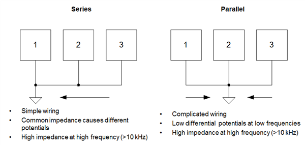
Single-point grounds present a problem whether in series or in parallel, as shown in Figure 5.

Figure 5: Series and parallel single-point ground connections

A better approach is to use multipoint grounding. As shown in Figure 6, multipoint grounding enables low impedance between circuits to minimize potential differences, and it also reduces circuit trace inductance. The objective is to contain high-frequency currents in individual circuits and keep them out of the ground plane.

Figure 6: Multipoint ground connections

Many buck converter control ICs recognize the noise and quiet circuit areas, and the IC pinout is such that the layout and component placement around the IC pins is easier. Some even provide a separate pin for power and analog ground, as shown in the TPS40170 60V synchronous buck pulse-width modulation (PWM) controller pinout shown in Figure 7.

Figure 7: Buck controller IC pinout for analog and power connections

So planning for the layout around the IC pinout and using the good layout practices mentioned in this post can help you get your buck converter design working right from the start, and avoid any headaches later. Check out TI’s buck converter and buck controller selection tables for a variety of buck DC/DC solutions.

Four tips to debug a boost converter

$
0
0

The most efficient way to solve a problem with a converter such as failure to startup, output voltage unstable, etc. is to do some basic debugging. Basic debugging would rule out some obvious problems, like fault assembling or the wrong components and, the debugging data can help support engineers of TI to find the root cause quickly.  In this blog post, we will talk about tips for debugging a boost converter.

Check the problem in another board

If you observe a problem in one boost converter board, your first action should be to confirm the behavior in another board. If only one board behaves abnormally, the problem may be caused by bad soldering or damage to the IC.

The soldering problem can happen when either the IC or its external components are soldered on. There are two kinds of bad soldering. One occurs if the adjacent pins short together; the other occurs if a pin and its pad aren’t soldered well. Measure the resistance between the adjacent pins to rule out the former problem, and measure the internal diode to rule out the latter problem.

Figure 1 shows the internal diode between the GND pin and the other pins in the IC. You can use a multimeter to test this diode and check for a soldering problem. The multimeter will show approximately 0.7V if the soldering is good. For some special pins, there may be two diodes in series instead of one. In those cases, the multimeter will show 1.4V.

Figure 1: Diode between VIN and GND pin

You can check for IC damage by measuring the resistance between the GND pin and any other pins during power off. The circuits (internal or external) connected to the pins may be damaged if the resistance is much lower than the normal ICs. The damage is mostly caused by voltage overstress, which may result from electrostatic discharge (ESD) because of mistaken handling, bad printed circuit board (PCB) layout or a high voltage out of the IC’s specification from an external source.

Check the schematic and components selection

Double-check the schematic again to see if the external components are within the datasheet recommendations. The inductor and the output capacitors are the key components for a boost converter. The inductance and capacitance should be within the value range recommended in the datasheet. You can find the suggestions in the “Recommended Operating Conditions,” “Inductor Selection” and “Capacitor Selection” sections of the datasheet. Figure 2 shows the recommended operating conditions for TI’s TPS61253. The suggested effective capacitance ranges from 3.5µF to 50µF. The suggested inductance is from 0.7µH to 2.9µH.

Figure 2: Recommended operating conditions for the TPS61253

A ceramic capacitor’s effective capacitance is related to its DC bias voltage. For example, the effective capacitance of a 10µF/0603 capacitor, such as the GRM188R60J106ME47 from Murata, is only 3µF at a 5V bias voltage condition. The current flowing through the inductor should be below the saturation current at any condition. Otherwise, the inductance may decrease below the recommended range, which could cause unexpected problems.

Check the layout

Bad PCB layout causes many problems: IC damage, high output ripple, low output-current capability and more. The damage is mostly caused by a high voltage spike at the SW pin, which overstresses the internal power MOSFET of the IC. (See the user’s guide, “Five Steps to a Good PCB Layout of a Boost Converter,” which describes a method for boost converter PCB layout.) The datasheet and IC user’s guide should also provide a layout pattern example.

The output capacitor is the most critical component in the PCB layout. If you see a problem and the routing of the output capacitor is not good, try placing a 1µF ceramic capacitor close to the IC and connect them with a minimum loop. You’ll know the root cause if this method resolves your problem.

Check the operating waveform

The operating waveforms of the converter can be very helpful when seeking the root cause of a boost converter problem. The waveforms of the VIN pin, SW pin, VOUT pin and inductor current are the most important. Figure 3 shows a method for measuring inductor current: insert a wire in series with the inductor and use a current probe to measure the current flowing through the wire.

Figure 3: Measuring the inductor current

Measure the four waveforms in the same picture if possible. Figure 4 shows the waveforms of the TPS61258 at light and heavy load conditions. In the waveforms, CH1, CH2, CH3 and CH4 are VOUT, SW, VIN and ICOIL (inductor current), respectively. CH1 is set to DC coupling with a 5V DC offset. So you can easily check both the DC voltage and AC ripple of the TPS61258 output voltage.

At light load conditions, the TPS61258 operates in power-save mode, during which the device switches several cycles and stops for a period of time. At heavy loads, the TPS61258 keeps switching with a 3.5MHz frequency.

During device switching, ICOIL increases linearly when the switch is approximately 0V and decreases linearly when the switch is approximately 5V.


Figure 4: Operating waveforms of the TPS61258 (CH1 VOUT, CH2 SW, CH3 VIN, CH4 ICOIL) at light load, in power-save mode (a); and at heavy load (b)

One device may operate abnormally if its operating waveform is not similar to the waveforms in Figure 4. You can determine the root cause of the problem from the waveform, such as current-limit trigger, device unstable, VIN out of the specification, etc.

Record the debugging data and contact support

These four tips should help solve most basic problems. However, they may be not enough to solve a complex problem that relates to the whole system power design. In those cases, you may need to contact a TI field application engineer or post the problem in the TI E2E™ Community. It is a good habit to record the experimental data and waveforms while debugging the circuit. The data and waveforms will help a TI engineer find the root cause efficiently.

More suggestions

A simple converter could help avoid many problems from the beginning. TPS61xxx series boost converters are highly integrated, easy-to-use devices. A fixed output-voltage converter such as the TPS61253 requires only three external power components: an input capacitor, inductor and power inductor, as shown in Figure 5. Just follow the datasheet recommendations for component selection and PCB layout. You can implement the required boost converter easily.

Figure 5: TPS61253 boost converter schematic

The next time you are debugging a boost converter, refer to the tips discussed in this blog for help.

  • Confirm the problem in other boards.
  • Double-check the schematic and external components.
  • Double-check the PCB layout.
  • Measure the operating waveforms to observe abnormal behavior.
  • If you still haven’t resolved the problem, record the experimental data and ask TI for help on the E2E Community Non-Isolated DC/DC Forum.

Please share your experiences debugging a boost converter in the comments section below.

When should you use PWM controllers?

$
0
0

 PWM is a control method that can be applied to many power-supply topologies. And because power supplies, regardless of topology, are used in an endless set of applications, they have the reputation of being used everywhere; PWMs are used in a wide variety of applications.

PWM is short for pulse-width modulation. In the context of a switched-mode power supply, PWM is the scheme used to regulate an output such as an output voltage and reject variation from the input voltage to a system. This system concept describes a switched-mode power supply. The inputs and outputs can be DC, sinusoidal (AC) or even some other periodic waveform.

Consider two very popular PWM controller families, the UC3842/UC3843/UC3844/UC3845/UC3846 (UCx84x) and the UC1525A/UC2525A/UC3625A (UCx525A). Figures 1 and 2 show these families’ block diagrams, respectively.

Figure 1: UCx84x block diagram


Figure 2: UCx525A block diagram

Both figures highlight a common PWM control method, where an error signal compared to a fixed-frequency ramp produces a PWM output that drives the switches in a switched-mode power-supply topology. The error signal can control current, voltage, both current and voltage, or some other significant property in the end application. The topology can involve a single switch, as found in buck, boost, flyback or forward topologies; the UCx84x is a good PWM controller to consider for these types of topologies. Consider the Ucx525A for topologies (excluding synchronous rectification) that have more than two switches, like the Fly-Buck™ converter, active clamp forward, push-pull or half bridge. At times, a MOSFET gate driver is needed in order to drive the MOSFET. These two families of PWMs are very basic controllers, with uncomplicated logic and just the right amount of extra features, making them easy to implement in many applications.

Applications with PWMs include welding, appliances, motor drives, personal electronics, inverters, electric vehicles, uninterruptable power supplies, solar power, audio amplifiers and car heaters. In general, where switched-mode power supplies are used and you don’t need the complexities of a more advanced topology, think about using a simple generic PWM controller.

Using your favorite PWM controller in many applications can decrease development time while you build power-supply design confidence with a set of proven designs tucked up your sleeve. One final advantage in using a PWM is that it can be leveraged across multiple designs, keeping your procurement team excited about a high-volume sourced component.

Improvements in the process technology used to manufacture the generic purpose PWM controllers from a bipolar technology to a current Bi-CMOS technology can improve critical design parameters. A quick comparison between the UC284X/UC384X and the UCC28C4X/UCC38C4X details improvements due to the process change on a controller architecture that has remained the same: lower supply current from 11 mA to 2.3 mA at 50 kHz, rise/fall times from 50 ns to 25 ns and reference voltage accuracy from ±2 % to ±1 %. Even the operating frequency is increased from 500 kHz to > 1 MHx to name a few areas of improvement.

Visit our PWM and resonant controller overview page to see other PWM controllers and explore application and design ideas. You can also start a design in WEBENCH high voltage designer with TI’s high performance, current mode PWM controllers.

Additional resources

Viewing all 437 articles
Browse latest View live


<script src="https://jsc.adskeeper.com/r/s/rssing.com.1596347.js" async> </script>