Quantcast
Channel: Power management
Viewing all 437 articles
Browse latest View live

Stack current with PowerStack packages for higher power POL

$
0
0

 Voltage regulators, particularly DC/DC converters with integrated MOSFETs, have evolved from being simple, low-power supplies defined by input voltage, output voltage and current to now being capable of delivering much higher power, monitoring the environments in which they operate and adapting accordingly.

Historically, applications requiring currents greater than 10-15A generally relied on controllers with external MOSFETs to deliver the requisite power to do the job. Converters – enabling simpler designs with easier layouts and fewer components in their bill of materials (BOM), while also providing a high-density solution with high reliability – were relatively limited in the amount of power they could deliver.

Applications such as network routers, switches, enterprise servers and embedded industrial systems are increasingly power-hungry, requiring 30A, 40A, 60A or more for their point of load (POL). These applications are extremely board space-constrained when accommodating controllers and external MOSFETs.

Advancements in MOSFET and packaging technologies have enabled TI to successfully address these challenges. New-generation MOSFETs such as TI’s 2.x NexFET™ power MOSFET offer lower resistivity (RDS(on)) in a given silicon area for higher current capability. Our PowerStack™ package technology stacks the integrated circuit (IC) and MOSFETs one on top of the other (see Figure 1) to offer converters capable of delivering 35A-40A per phase. Taking it to the next level, TI now offers converters such as the TPS546C23 SWIFT™ converter that can be current stacked (see Figure 2) to deliver up to 70A POL.

Figure 1: PowerStack package for high density.


Figure 2: Stacking two DC/DC converters for higher load currents.

Dealing with high-density power environments also raises system power optimization issues and the need for active power management (APM). For example, a 10% scaling of voltage in a 1VOUT 30A POL could impact package thermals by up to 0.5W! It’s important to avoid excessive thermals to stay within safe operating areas (SOAs) and not compromise system reliability. In order to properly manage power in real time (see Figure 3), it is crucial to monitor telemetry parameters such as current, voltage and temperature. TI’s new TPS546C23 converter with PMBus supports telemetry.

Figure 3: Fusion GUI to manage power supplies with PMBus.

Evolving from simple, low-power supplies to today’s DC/DC converters with integrated MOSFETs, voltage regulators have evolved to deliver much higher power and to monitor and adjust to environments. Now you can easily monitor, manage and stack TI’s TPS546C23 PowerStack converter to provide a high-density, high-performance POL up to 70A. Get more information and order an evaluation board.


Biasing an SR controller IC in USB smartphone charging applications

$
0
0

With the increased interest in energy efficiency and energy conservation, a synchronous rectifier (SR) helps boost efficiency when converting offline AC power into 5V for USB smartphone battery charging. During this conversion, an SR controller integrated circuit (IC) needs proper biasing in order to provide the adequate drive to the SR MOSFET. The bias voltage is typically above 4V in USB applications. Because the BC1.2 USB battery-charging standard specifies a power adapter output in the range of 4.1V to 6V, you can bias SR controller ICs from that output, as shown in Figure 1.

Figure 1: Flyback converter with the SR controller biased from the output voltage

What if the output voltage drops below UVLO?

This biasing approach is simple, easy and has almost no additional cost. It works well when the output voltage is above 4V, but at <4V on VDD, the SR controller IC enters undervoltage lockout off (UVLO). The issue here is that the SR still needs to be operational when the output drops below 4V. In fact, it still needs to be operational before the output drops to 3V in USB smartphone applications. This is because battery-charging operations require constant-current operation, where an adapter keeps delivering constant current while its output voltage falls to help operations such as battery charging during dynamic power management (DPM).

Figure 2 illustrates typical 5V-3A power adapter output characteristics. Operation ceases when the output drops to 3V because at 3V, the lithium-ion battery cannot charge; thus, no bias power is necessary for the SR. As a matter of fact, a fault is actually identified when high current is present at ≤3V.

Figure 2: Typical 5V-3A power adapter output characteristics

When the output drops below 4V, the SR turns off, which causes undesired performance. First, the SR turn-off causes a constant current shift due to the voltage increase from the body-diode conduction, leading to unnecessary transients. Second, the current flowing through the SR MOSFET (QSR) channel now flows through its body diode. The resulting higher-power losses may cause a temperature rise that could cause thermal runaway and damage. Therefore, you need alternative approaches to keep the SR on before the output drops to 3V.

Biasing an SR controller using a charge pump

One alternative is to use a charge-pump circuit. Figure 3 explains the operation of a charge pump with the circuit. The VDD voltage on capacitor C2 is brought up to 2x Vp by switching S1 and S2  will alternate switching on/off, when the Vp pin is connected to the adapter output after the detected output voltage drops below 4V. As the output is between 3V and 4V, the SR bias voltage VDD is maintained at 6V to 8V, thus achieving the desired SR bias voltage.

This approach needs additional components and control functions to set up proper timing for S1 and S2. You can integrate these components and control functions inside an IC to simplify application designs, but you will still need three dedicated pins and a capacitor (C1) to fulfill the function.

Figure 3: Charge-pump biasing

Biasing an SR controller using a linear regulator

The SR MOSFET drain pin is applied with a pulse train during flyback converter operation. The pulse magnitude is well above 4V in USB smartphone power adapter designs. Figure 4 shows a linear regulator that can be used to regulate the linear regulator output to 5V which is connected to the SR controller VDD pin. But because you have to add four additional components, this approach becomes less attractive due to the increase of both cost and board space.

Figure 4: Pulse linear-regulator biasing

Biasing an SR controller using a simple regulator

As these first two approaches are generally not preferable in USB smartphone charging applications given their cost and complexity, newly developed SR controller ICs such as the UCC24636 accept a simpler bias approach using a “simple regulator,” as shown in Figure 5.

Figure 5: Simple regulation bias


The bias VDD pin accepts a wide voltage range from 4V to 30V – and the driver output is internally clamped to the MOSFET’s gate-voltage level, 10V. These features enable a simple regulator (placed externally with a diode and a resistor) to charge the VDD capacitor to a proper level across the input and load range. When the drain pin voltage is pulsing, the diode (D) rectifies the pulses, while the resistor (R) and capacitor (C) average out the pulses to deliver DC voltage and power to VDD.

Table 1 provides biasing results based on the TI Designs Universal AC Input to 5V/3A Output Reference Design, which employs the UCC28704 and UCC24636, a universal offline input, and a 5V-3A output flyback converter.

Table 1: Simple regulator biasing results

The results depict a minimum controller VDD voltage above 4.57V even if the converter output drops to 3V, thus maintaining plenty of bias voltage to keep the UCC24636 in operation.

When converting offline AC power into 5V for USB smartphone battery charging, an SR controller can help boost efficiency when biased properly.

Additional resources:

Don’t leave it floating! Power off your outputs with quick output discharge

$
0
0

When a semiconductor lists quick output discharge (QOD) as a feature, it will quickly discharge the output when the device is disabled (or in an “off” state). In other words, when VOUT is disconnected from VIN, VOUT will instead be connected to ground through internal circuitry, preventing the output from “floating” or entering into an undetermined state. Figure 1 shows a simplified block diagram of QOD circuitry.

Figure 1: Block diagram of a load switch, with QOD circuitry in blue, showing the discharge FET, inverter and discharge path from VOUT to ground. The soft-start capacitor is also shown in blue.

The main benefit of adding QOD functionality to a system is simple: any power rail on VOUT of a QOD-enabled device will be at a known “zero” or “off” state when the device is disabled. This ensures that when you are designing your system – and especially when you are working out the timing for your power sequencing – that none of your power rails are left floating. Knowing the state of all power rails in your system (and thanks to QOD, knowing that they are actually turned off/grounded), allows you to reduce the number of “variables” in your design, lowering the risk of your design not working as intended.

How to implement Quick Output Discharge in your next design

The easiest way to implement QOD is to include a device which has the functionality already integrated inside. As an example, Figure 2 shows how the TPS22915 load switch implements QOD.

Figure 2: Simplified block diagram of the TPS22915, outlining QOD circuitry

All load switches with QOD functionality contain an additional FET between the VOUT pin and ground pin (GND), as shown by the dotted outline in Figure 2. This creates a pull-down resistance to quickly discharge VOUT to ground. While some devices like TPS22918 allow you to place your own discharge resistor, most have an integrated, fixed QOD resistance. As the QOD resistance will vary for each product, you can use Equation 1 to calculate the exact QOD resistance needed for your specific power down sequencing application. 


where Vf is the final VOUT voltage; Vo is the initial VOUT voltage; R is the value of the output discharge resistor; and C is the output bulk capacitance on VOUT.

Can you add QOD to a device that does not already integrate this feature? In some cases, you can multiplex certain pins of devices to provide additional functionality. One such example is the BFET pin of the TPS25924 eFuse. This pin normally drives an external blocking FET to protect a system against reverse current, as shown in Figure 3.

Figure 3: Adding reverse-current protection with an external blocking FET on the TPS25924’s BFET pin

You can reconfigure this pin to provide QOD functionality even though it is not integrated. This can be accomplished through a very similar circuit, as shown in Figure 3, replacing the blocking FET with a discharge resistor (RDCHG in Figure 4).

Figure 4: Adding QOD functionality using the TPS25924’s BFET pin

Keep in mind that while QOD is beneficial in most situations, it is not always good to have. In power multiplexing applications, the QOD circuitry would create a constant path to ground on the output of the multiplexer. Additionally, if a supercapacitor is on the output of a power switch, that switch better not have QOD! If it does have QOD, it will drain the supercapacitor’s stored charge, wasting energy. Check out our load switch portfolio, which contains devices both with QOD and without QOD functionality, facilitating any power design.

 Additional resources

How to approach a power-supply design – part 1

$
0
0

Switch-mode power-supply design can be a mysterious thing if you do not know how and where to start, because there is a great variety of topologies and controller types from which to choose. In this blog series I will describe how to pick the most fitting power supply topology for your application and what you need to know to get there. The best starting point is usually a dedicated specification for your application. This specification should at least include information about the input-voltage range, output voltage and maximum load current. However, choosing the best-fitting topology and/or system solution will be easier if you can also answer some of the subsequent questions:

  • Does your application need an isolation barrier between the input and the output? If yes, which insulation level do you need? Do you want to achieve your output-voltage regulation with primary- or secondary-side regulation?
  • Is your power supply intended for DC-to-DC or for AC-to-DC conversion? Additional helpful information regarding the input can include the maximum in-rush current, the maximum input current and the maximum acceptable reflected ripple.
  • What is the output power range for your application? In many cases, this information will decrease the number of usable topologies and controllers. Your specification should also include requirements for the power supply’s output-voltage tolerance, maximum acceptable output-voltage ripple, average output current and peak output current. Additional demands for dynamic behavior like load regulation, transient response and line regulation (the latter is important for automotive cranking, for example) should also be in the specifications, because you might need to adjust your power stage accordingly to achieve them.
  • What is your desired switching frequency? Do you need frequency dithering to lower peak emissions? Do you have more than one power supply in your system? If so, do the supplies need to be synchronized? For automotive applications, it is common practice to choose a switching frequency below 450kHz or above 2.1MHz to avoid interference with the AM band. For high-power applications, you might want to choose a low switching frequency for the best possible efficiency.
  • What is the ambient and working temperature range? Which application segment is the design for? Are automotive or military-grade parts required?
  • What is the main priority for your power supply? In general, for every power-supply design, you have to make trade-offs between performance, form factor and cost. It is important to know which of these factors has the highest priority, because it will directly impact the quality of your design.
  • Does the power supply need to meet certain standards regarding efficiency, electromagnetic interference (EMI), power factor correction (PFC) or Underwriters Laboratories (UL) qualification? Is light load efficiency or a specific standby power level required?

Of course, all of this information is not always necessary. The more detailed your power-supply specification is, however, the easier it is to pick the best-fitting topology and the best performing components.

The most common switch-mode power-supply topologies are:

  • Buck.
  • Boost.
  • Inverting buck-boost.
  • Single-ended primary-inductance converter (SEPIC).
  • Ćuk.
  • Zeta.
  • Flyback.
  • Two-switch flyback.
  • Active-clamp forward.
  • Single-switch forward.
  • Two-switch forward.
  • Push-pull.
  • Weinberg.
  • Half bridge.
  • Full bridge.
  • Phase-shifted full bridge.

These topologies are supported by TI’s Power Stage Designer 3.0 tool.

Table 1 summarizes the most common parameters for power supply specifications.

Input

  • DC/DC or AC/DC
  • Voltage ripple
  • In-rush current

Output

  • Voltage tolerance
  • Voltage ripple
  • Average current
  • Peak current
  • Transient response
  • Load regulation
  • Line regulation

Isolation

  • None
  • Functional
  • Reinforced
  • Double
  • Safety category

Priority

  • Performance
  • Form factor
  • Cost

Switching frequency

  • Range
  • Synchronization
  • Dithering

Standards

  • EMI
  • PFC
  • UL
  • Efficiency
  • Light load efficiency
  • Standby power

Table 1: Summary of helpful specification parameters

In my next post, I will describe how to pick the most fitting topology based on the parameters of your specification.


Additional resources:

The top three ways to split a voltage rail to a bipolar supply

$
0
0

Audio applications, data-signal acquisition and analog sensors benefit from a bipolar bias power supply. A bipolar supply provides the best use of the analog-to-digital converter’s (ADC) dynamic range, enables rail-to-rail amplification, isolates the analog signal from ground noise and offers many other benefits. In this post, I’ll describe three ways to split a single supply rail into a bipolar voltage rail. Table 1 shows the advantages and limitations of each of the three most common methods of splitting a single positive-polarity voltage rail into a bipolar rail.

Table 1: Split-rail method comparison table

The first (and simplest) method is to create a virtual ground by implementing a resistor divider; unfortunately, this configuration is susceptible to becoming unbalanced at very low loads. The TLE2426, shown in Figure 1, creates a common ground buffered from the source; the buffer creates a more stable center point between the rails under load condition. The disadvantage is that it can only handle a few tenths of milliamps.

Figure 1: Simplified schematic of the TLE2426 virtual ground driver in a split-rail configuration

Switching topologies offer higher efficiency, accuracy and stability, as well as more features than a discrete approach. There are two categories of switching regulators: inductive and capacitive (that is, a charge pump or switched capacitor). Inductive regulators are the most efficient devices, but are more complex and require an inductor, increasing bill of materials (BOM) cost and total solution size. Figure 2 shows a typical schematic for the TPS65133, a boost converter with a bipolar output capable of supplying a ±250mA output current with 90% efficiency for most input and output voltage configurations.

 Figure 2: TPS65133 boost converter with dual output voltage

Another popular inductive split-rail solution is a fly-buck topology, which is a step-down synchronous buck converter with a coupled inductor in the feedback loop; this topology offers an isolated voltage supply. The fly-buck method is a more complex technique: for step-by-step details, see the application report, “Creating a Split-Rail Power Supply with a Wide Input Voltage Buck Regulator.”

Charge pumps are a popular and easy way of inverting positive rails. You can create a split rail by combining a charge pump with LDOs or DC/DC boost converters, as shown in Figure 3.The LM27761 inverting charge pump in Figure 3 has an integrated adjustable negative LDO capable of supplying 250mA; you can adjust the output voltage using external resistors.

Figure 3: Split-rail solutions combine an inverting charge pump and a positive voltage regulator

TI also offers integrated solutions like the TPS65133, which is a boost converter with an integrated LDO and an inverting charge pump capable of supplying ±5V at 90% efficiency. For step-down split-rail applications where you must minimize noise, ripple, cost and space, the LM27762 charge pump has integrated positive and negative LDOs. Again, you can adjust the output voltage with external resistors. The LM27762 requires only a few compensating elements, as shown in Figure 4.

Figure 4: The LM27762 split-rail charge pump with integrated LDOs

In this post, I covered the top three ways to split a voltage rail into a bipolar supply. The discrete solution is a simple solution but is limited on output current, voltage regulation and stability. Inductive switchers have great efficiency, high output current and are capable of isolating the output supply, but the total BOM cost and total solution size are high. Combining the charge pump and LDOs offers low noise, high power supply rejection ratio (PSRR) supply, low cost and small size, but cannot provide currents as high as the inductive solution. Regardless of your application requirements, TI offers a variety of bipolar supply reference designs to get you started on your next design.

Additional resources


Which is better? Discrete or combined controllers for an AC/DC power supply?

$
0
0

If you have ever listened in on typical hallway conversations in a power-supply design company, it’s likely you have heard a spirited debate on whether the right way to design a >75W power supply involves the architecture shown in Figure 1 or Figure 2. The power-supply components in both cases are exactly the same; the only difference is the controller.

Figure 1: Discrete controller IC-based AC/DC design


Figure 2: Combo controller IC-based AC/DC design

Texas Instruments has supporters on both sides of the debate, and a track record of products to back both solutions.

Notwithstanding the length and breadth of TI’s product portfolio in the combination or “combo” controller space and the ability to get more features within the same solutions, I still subscribe to the argument that in the long run, a stand-alone power factor correction (PFC) controller followed by a stand-alone DC/DC converter offers an unparalleled set of advantages for engineers designing a wide range of applications, especially in the current cost-conscious consumer space.

Layout

Most power-supply designers will tell you that the technical aspect of the power-supply design that comes back to haunt them most is the printed circuit board (PCB) layout. A bad layout is a good recipe for a one-way ticket to Nowheresville. Power supplies come in all shapes and sizes, and require very different layout considerations depending on the form-factor requirements.

Figure 3 shows the form-factor-compliant Slim 150 Watt LED TV Power Reference Design. Note that there is a fair amount of space between components. Also, the “slim” requirements in a television force the layout to be ultra-low profile, making the large components on the board look like my son’s kindergarten class during recess/naptime. The PFC stage and inductor-inductor-capacitor (LLC) stage are far away from each other, making it extremely hard for a combo controller to have an optimal layout. Discrete solutions have no such problem, since the controllers reside right next to their respective power-stage components.

Figure 4 displays the form-factor-compliant High Efficiency 350W AC/DC Power Supply Reference Design for industrial power supplies. Here is a space-constrained design that looks more like downtown Dallas than a low-cost two-layer PCB layout. Having a single combo controller to which signals are routed is no different than wanting a single massive parking lot catering to the whole of Manhattan fed by single-lane alleys ... good luck getting in and out.

The uniqueness of power-supply requirements and the one-size-fits-all nature of combo controllers fundamentally do not jive. Some power supplies are constant current, some are constant voltage, some require high total harmonic distortion (THD), some require low standby, some are meant to be fixed load – but almost none need all of these things. Using such a solution for your application can become a bit of overkill."Some power supplies are more equal than others"

As long as the diversity of the power supplies continues to exist, there will always be logical reasons where a 2-IC solution may be a much better fit for your applications and the coffee pot in the hallway nearest to my desk will continue to get its broad patronage…

Discover the controllers that TI is currently offers to target these applications. 

What is a watchdog timer and why is it important?

$
0
0

Much like a small, yappy dog that lives in a celebrity’s purse, watchdog timers are often considered unnecessary or excessive. To equate the two, how ever, would do a great disservice to the watchdog. Unlike “purse dogs,” watchdogs add critical monitoring features that allow you to internally and externally monitor your system for failure and take action should that happen.

Just what is a watchdog timer?

Simply put, a watchdog timer is a device that asserts a reset output if it has not received a periodic pulse signal from a processor within a specific time frame. One way this is implemented is by a digital signal output (GPIO) from the processor feeding into the watchdog input (WDI) of an external watchdog timer as shown in Figure 1. TPS3851 is a supervisor with an integrated watchdog timer. This allows it to both supervise the supply rail to the microcontroller and monitor the digital pulse emanating from the MCU in an external fashion.

Figure 1: Watchdog monitoring provided by the TPS3851

The processor periodically sends a pulse to the watchdog timer to indicate that the system software is operating properly. If the watchdog timer does not receive this pulse within an allotted time frame (known as the watchdog timeout), the watchdog timer asserts a reset output. This reset output can be used to notify the system that the processor has experienced a hang or a freeze, or to reset the processor itself. Figure 2 illustrates a pulse received within the watchdog timeout and a pulse received after the watchdog timeout has expired.


Figure 2: Operation of a standard watchdog timer

Why are watchdog timers so important?

Watchdog timers provide a method for alerting a system or resetting a processor whose software has experienced a freeze or hang. While no one purposely designs software to freeze, good system designers plan for failures anyway – as it’s always better to prepare for the unexpected. Without this monitoring, the processor could stay frozen indefinitely and lead to further system failure. An external watchdog timer with an adjustable timeout interval, such as the TPS3851, can identify these software freezes within just a few milliseconds and reset the system or processor appropriately. This functionality is especially necessary in embedded or remote systems where manually resetting the system isn’t practical or even possible.

How can I implement a watchdog timer in my embedded system?

There are two primary methods for implementing watchdog timers:

  • Using a processor with integrated watchdog functionality. Many microcontrollers such as the MSP430F5529 series have integrated watchdog functionality. This is valuable because it is very easy to implement and no other ICs are required. However, it comes with one major caveat: integrated watchdogs may not always work as desired because the code issues that cause the MCU to malfunction could also inadvertently disable the watchdog timer. Again, software is written in such a way that an internal watchdog should be able to detect any freezes or hangs. However, taking the extra steps to monitor the watchdog input in a redundant manner can help account for unforeseen errors in code.
  • Using a voltage supervisor with a watchdog timer. A supervisor with watchdog-timer functionality such as the TPS3851 or the TPS3110 allows you monitor both the supply voltage and watchdog signal in an external, redundant fashion. Should the internal watchdog of the processor fail to detect an errant or missing pulse, the external watchdog timer will add a level of detection not achievable otherwise.

In principle, the functionality of a watchdog timer is not overly complicated. However, its importance in maintaining the reliability of systems cannot be overstated. This is especially true if a human-initiated system reset in case of failure is not possible or very difficult.

Additional resources

Integrated power devices simplify FPGA and SoC designs

$
0
0

Industrial electronics are trending toward smaller board sizes, sleeker form factors and more cost-effectiveness. Due to these trends, electronic system designers must reduce the size and cost of printed circuit boards (PCBs). Industrial systems using field-programmable gate arrays (FPGAs) and system on chips (SoCs) require multiple power rails while being challenged with small size and low cost. An integrated flexible power device can offer a significant cost savings and solution size reduction for such applications.

An integrated flexible power device contains multiple DC/DC converters within the same package. These DC/DC converters could be any combination of buck converters, boost converters and/or LDOs in a single package. Figure 1 is an example functional block diagram, where the LM26480 includes dual 2MHz high-efficiency 1.5A buck converters and dual 300mA LDOs.

Figure 1:LM26480 functional block diagram

Let’s walk through an example that highlights the benefits of using an integrated flexible power device. Imagine designing the power-management system for a drone controlled by an SoC or FPGA. Figure 2 shows four components within this system that are a perfect match for a power-management IC (PMIC).

Figure 2: Discrete vs. integrated power-management comparison

Both power solutions shown will produce four separate rails that power the Global Positioning System (GPS), input/output, core voltage and double data rate type 3 (DDR3) of the system. In both options, a front-end switch-mode power supply efficiently bucks the voltage of the drone battery down to the 5V rail shown as the input to Figure 2. Discrete components can drop this 5V supply further, as shown in option 1, or an integrated device, as shown in option 2.

Imagine powering this system using four separate components: two LP3982 300mA single-channel LDOs and two TLV62084 2A buck converters. You can use these discrete DC/DC converters to power the system, although you will still need four separate active components. This may not be the most optimal solution, considering that active components have the highest reliability issues.

An alternative solution could be to use an integrated flexible power device that provides the desired voltage and current capabilities of the system with just a single IC. As Figure 2 highlights, this provides numerous benefits.

First, the integrated solution is 20% more cost-effective when compared to the discrete solution. Second, the PMIC solution requires 10% less board space compared to the combined board space of the four discrete devices. Third, the integrated device requires fewer external components than the discrete solution, which further decreases overall size and cost. And decreasing the bill of materials (BOM) device count can lead to increased reliability.

So consider an integrated flexible power device when designing systems that require multiple power rails, especially in applications requiring FPGA or SoC power.

Additional resources


How to overcome minimum on-time challenges in switching power supplies

$
0
0

In switching power supplies such as a buck converter, the duty cycle controls the output voltage with respect to the input voltage. While a higher switching frequency is great for reducing the solution size by enabling the use of a small inductor, there is a minimum on-time that must be satisfied in order for the switching power supply to function properly. In other words, the high-side FET must be turned on for a certain amount of time within each switching period such that the condition in Equation 1 is met:

where D is the duty cycle and fs is the switching frequency.

Several factors within the circuit necessitate this minimum on-time. For example, one factor is the current spike on the leading edge of the current waveform in the high-side FET. Since the FET has parasitic gate capacitances Cgs and Cgd, and the current through the high-side FET changes abruptly when it turns on, the capacitances behave similarly to a short in the presence of the changing current. This results in a current spike. In order to prevent this from triggering the current limit, current-limit violations are ignored during blanking time (tLEB in Figure 1). Therefore, the minimum on-time of the switching circuit must be larger than the blanking time – otherwise, the current-limit protection will be turned off for longer than the actual on-time.

Figure 1: Current spike on the leading edge of the current waveform of the high-side FET

Other factors include the rise and fall time of the switch-node voltage and level-shifter delay to set the gate voltage on the high-side FET.

Devices will behave differently when the on-time falls to its minimum, sometimes resulting in problems that may seem unexpected. For example, the switching power supply may start pulse skipping (shown in Figure 2) as a way to compensate for the inability to further decrease the on-time while still maintaining the output voltage. This results in a larger output voltage ripple and unknown harmonics from changes in switching frequencies.

Figure 2: Pulse-skipping waveform in the TPS61175 boost converter

Other devices may instead use frequency foldback to allow the duty cycle to decrease. In this case, the switching frequency drops but the pulses occur regularly – unlike in pulse skipping where entire pulses are dropped. Figure 3 shows an example of this functional mode.

Figure 3: Frequency foldback in the LM53602 at VOUT = 5V

It is critical to note these issues when choosing a device to use for your switching power-supply needs. For example, in automotive applications, frequencies within any circuit must not fall within the AM band. Otherwise, they may interfere with the radio signal and clobber any information that was sent via that frequency band. Any application that involves information transfer on a certain frequency band must pay special attention to the possibility of interference from the regulator. Designs that use devices with a smaller minimum on-time will therefore encounter fewer complications.

One example of a great device with a small minimum on-time is the LM53602 buck converter. Its minimum on-time of 50ns enables a larger range of possible duty cycle and frequency pairings. As long as switching power-supply designers are cognizant of the significance of minimum on-time, their designs will be able to work more effectively in a larger variety of situations.

Upgrading USB chargers from Type-A to Type-C

$
0
0

USB chargers are becoming more and more prevalent, and seem on their way to becoming universal. They’ve gone from just being on your computer to being in wall outlets, wall warts, car panels, airplane seats, and more.

Traditional USB Type-A chargers have just one voltage, which lends itself to a simple high-level design. Figure 1 shows a simplified schematic. The resistor divider formed by RFBL and RFBU enables closed-loop regulation of the output voltage applied to VBUS. In this topology, the flyback controller must limit the output current for safety.

Figure 1: Traditional USB charger schematic for Type-A receptacles

USB Power Delivery (PD) on the USB Type-C™ connector enables higher power charging, which will broaden the USB charging ecosystem even more. However, USB PD and USB Type-C have new requirements, for which the schematic in Figure 1 is not sufficient.

Figure 2 shows a simplified schematic for a USB PD charger. Right away, you can see that there are two MOSFETs in the power path and a bulk capacitance that were not there in Figure 1. Notice also that this schematic can deliver multiple voltages. The PD controller negotiates voltages over the configuration channel (CC) and then pulls the CTL1 and/or CTL2 pins low to adjust the resistor divider to get a voltage higher than 5V. The CTL pins are either pulled to ground or set to high impedance by the PD controller to select the desired output voltage.


Figure 2: USB Type-C PD charger schematic for Type-C receptacles

USB Type-C has some requirements that are different from USB Type-A. Table 1 summarizes the two new requirements discussed here and their implications.


 Table 1: New requirements for VBUS in USB Type-C PD chargers

The first new requirement is that USB PD-capable chargers must be cold socket; in other words, VBUS is at 0V when the plug is empty. Also, when faults occur, the source is required to drive VBUS to 0V for close to 1s as it performs a USB PD Hard Reset. Driving VBUS to 0V requires a way to disconnect the flyback output from the VBUS on the connector while maintaining the PD controller supply. The schematic in Figure 2 uses the Q1 FET to allow VBUS to go to 0V, while the PD controller keeps its supply input (VPWR) high so that it can monitor for a sink attachment on CC1 and CC2.

In the USB specification, “0V” really means less than 0.8V (referred to as vSafe0V in the specification). This ensures that any attached USB device or sink detects that VBUS has gone away and resets. Although the USB specification requires USB self-powered peripherals to detect anything other than transients below 4.0V as a detach (USB 3.1 Section 7.5.1.2.4), it does not specify the detach voltage for other peripherals. It is common for USB devices to operate at even lower voltages. Therefore, the 0.8V definition ensures that all devices detect the detachment.

The second new requirement is that the Type-C receptacle cannot expose more than 10µF to VBUS when the receptacle is empty. The schematic in Figure 2 uses the Q2 FET to block in-rush current into CBULKC. Q2 divides the capacitance so that CPDIN applies directly to VBUS on the connector, and CBULKC is isolated from the connector. Since USB PD may provide up to 100W, the CBULKC capacitance may be very large. The USB 3.1 specification gives several reasons to limit capacitive in-rush, including limiting contact arcing to prolong the life of the connector (see USB 3.1 Section 11.4.4.1), which led to requiring USB Type-B ports limit capacitance exposed on the VBUS pin of their receptacle to 10µF.

The USB Type-C specification defines cables that adapt a legacy A plug to a C plug (see Figure 3), meaning that the hot VBUS from a Type-A receptacle can be connected to VBUS of the USB Type-C receptacle. Therefore, to protect legacy Type-A ports, all Type-C receptacles must limit their capacitance while not sourcing VBUS to the same 10µF limit for Type-B ports.

Figure 3: USB Type-A plug to USB Type-C plug 

Finally, a USB PD charger has the option of implementing a captive cable. A captive-cable product has a Type-C plug instead of a Type-C receptacle. The USB Type-C specification does not define a Type-C receptacle (female) to a Type-A plug (male). Therefore, the capacitance on the VBUS pin does not need to be limited since it is not meant to be mechanically connected to a Type-A port. This leads to the optimization shown in Figure 4, where the Q2 FET has been removed but the Q1 FET remains so that VBUS can be driven to 0V. Another benefit of the captive-cable application is that it only needs one CC pin, since the Type-C plug only has one CC pin.

Table 2 summarizes the applicability of these two new requirements for different applications.  

Table 2: Applicability of new requirements

For systems where Q1 and/or Q2 are required (i.e., all USB PD applications), system designers can minimize the system impact by selecting FETs with smallest RDS(on). Since N-channel MOSFETs generally offer lower RDS(on) than P-channel MOSFETs, it is best to select a PD controller that can directly control N-channel MOSFETs such as TI’s recently released TPS25740 and TPS25740A USB PD controllers.


Figure 4: USB Type-C PD charger schematic for Type-C plug (captive cable).

As with all new technologies, there are many details to be considered when developing a USB Type-C charger. It is not just a copy-paste from an existing USB Type-A product. Download a USB Type-C charger reference design today and upgrade your USB design for higher power charging. 

Additional resources:


Understanding undervoltage lockout

$
0
0

I'm told that the optimum environment for the human body is somewhere between 21°C and 30°C degrees, so inside TI’s air-conditioned office – set year-round to a toasty 23°C – conditions are perfect to deliver optimum performance (at least, that’s what my boss tells me).

In wintertime in central Europe, however, temperatures can fall to –20°C or lower. Even with many layers of clothing, the human body does not operate well under these conditions: it can survive, but it does not achieve optimum performance.

The human body is not the only thing affected by its operating conditions. Integrated circuits also operate best within certain temperature and supply-voltage ranges. In this post, I’ll discuss the latter, and the related undervoltage lockout (UVLO) function.  You can find more details in the application report, “Understanding Undervoltage Lockout in Display Power Devices.”

How low can you go?

As most electronic engineers already know, many integrated circuits contain an UVLO function that disables the device when its supply voltage is too low for correct operation. Without a UVLO function, at low supply voltages the device may do something, but you cannot be sure what. A UVLO function makes sure that the device either operates according to its specification or does nothing at all.

Among other things, a low supply voltage can cause:

  • Bias circuits to operate incorrectly.
  • Bandgaps to generate the wrong reference voltage.
  • Logic functions to fail.
  • Power transistors to turn on or off only partially.

Many devices have a UVLO threshold below a couple of volts. To be honest, it’s impressive that devices do anything at such low supply voltages. If you don’t believe me, try designing an analog circuit that operates from 2V and see how you get on.

The challenges are even greater in power devices. When the supply voltage is low, perhaps you can turn a power MOSFET on and off, but you can’t do it very quickly. And typically, the MOSFET’s on-resistance will increase, because the supply voltage is too low to generate a high-enough gate-source voltage.

Some devices specify a recommended supply-voltage range as well as a UVLO threshold. The device achieves full performance only if its supply voltage is in this range. But what happens between the UVLO threshold and the recommended minimum supply voltage? In TI’s display power group (the product line I work for), devices still function in this range, but we do not specify their performance. That means that buck converters still buck and boost converters still boost, but the output power available may be less than the maximum the device is capable of.

In mission-critical applications, UVLO thresholds are typically above the minimum recommended supply voltage – the device turns on only when it can achieve full performance. This approach leads to extremely robust system designs, but in general is not cost-effective for consumer products. It would be like driving a car that stopped working as soon as the fuel level got low (but not empty). It’s more useful to have the car still drivable – albeit with reduced performance – than to suddenly stop working altogether.

Figure 1 illustrates the operational state of a typical power device. You can see that:

  • In the red region where VI< VIT (min), the device does not operate and consumes minimal supply current.
  • In the green region where VI> VREC (min), the device operates with full performance.
  • In the gray region where VIT (min) < VI< VIT (max), the device is either off (red) or functional (yellow), but either state depends on the precise threshold of the UVLO function.
  • In the yellow region where VIT< VI< VREC (min), the device is fully functional but its performance is not specified in the data sheet.


Figure 1: Typical UVLO behavior

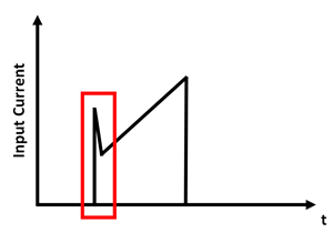
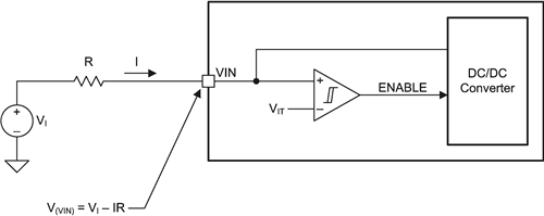
Note that the rising and falling UVLO thresholds are different. That is because a well-designed UVLO function has hysteresis. Why? Well, not only do comparator circuits in general benefit from hysteresis, power devices by their very nature tend to pull significant current from the upstream power supply. And since there’s always some resistance between the power supply and the device it’s powering, the voltage that the UVLO comparator sees is always a bit less than the voltage of the upstream power supply (see Figure 2). When the voltage reaches the UVLO threshold, the device turns off and the current flowing into it drops instantaneously to almost zero, causing the voltage that the UVLO comparator sees to immediately increase (because when the input current drops, the voltage drop across the input resistance suddenly disappears).


Figure 2: Equivalent circuit of a typical power device with UVLO function

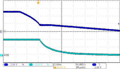
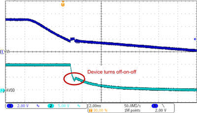
If the hysteresis voltage is smaller than I×R, under certain conditions the power management IC (PMIC) can turn on and off a number of times before it finally turns off for good. At best, this looks ugly; at worst, it can cause system-level problems. Figures 3 and 4 are scope plots illustrating this phenomenon.


Figure 3: Low-input resistance results in regular power-down behavior


Figure 4: High-input resistance results in irregular power-down behavior

The next time you're designing an application circuit, take a moment to make sure that you understand how the UVLO function works. For example:

  • Make sure that you know the circuit’s rising and falling thresholds and its hysteresis; if not stated in the data sheet, feel free to ask for more details in the TI E2E™ Community non-isolated DC/DC forum.
  • See if there’s a region between the UVLO threshold and the recommended operating voltage range in which the device can operate but perhaps not deliver all of its specified performance. Make sure that your application can handle this region.
  • Remember that the input current multiplied by the input resistance should be less than the UVLO hysteresis for clean power-up and power-down behavior. 

Additional resources

Can I apply an output voltage to my DC/DC converter?

$
0
0

A somewhat common question that I receive on the TI E2E™ Community Non-Isolated DC/DC forum is, “Can I apply a voltage to the output of a DC/DC converter when that converter’s input voltage is not present?” Such a scenario typically occurs during manufacturing when programming a processor or microcontroller (MCU). In these cases, the system’s normal input voltage from the AC mains or battery is not present. So an external voltage is applied on the output just to power up the MCU in order to program it. Figure 1 shows a block diagram for a typical building automation system.

Figure 1: Block diagram of an MCU being programmed

Applying a voltage to the output of a step-down converter is definitely not a typical application scenario, so this situation requires thoughtful action. The device and the application must be kept safe during this event, and their functionality may be different than expected. While the application note, Testing tips for applying external power to supply outputs without an input voltage, has all of the details and most common solutions, here are seven key system-level points to assess in designs which have a voltage applied to their output.

  1. All circuits connected to the input rail of the step-down (buck) converter are powered from the applied output voltage. In almost all cases, the step-down converter’s high-side MOSFET contains a body diode that provides a path from the output to the input.
  2. There is reverse current through the device from output to input. This current must be kept within the device’s rating so that it doesn’t overheat.
  3. If enabled, the device may consume current. You must account for this, if the applied voltage’s current is measured and used for pass/fail testing in production.
  4. If disabled, the device may consume current. Some devices, such as the TPS62097, have an output discharge circuit that sinks current from the output when the device is off.
  5. The voltage rating of every pin on every device that sees the applied voltage is maintained. Hot-plugging the voltage can easily cause overshoots that violate the pin’s ratings.
  6. Boost mode is disabled; otherwise the device may be damaged. Boost mode is enabled when any step-down converter operated in forced pulse-width modulation (PWM) mode has a voltage higher than its setpoint applied on the output and lacks a sufficient load on its input. In boost mode, the step-down converter operates bidirectionally to sink the applied output voltage. This energy moves to the input, where the voltage increases. When the voltage is high enough, the device breaks.
  7. The power good (PG) output is in the expected state. Depending on the level of the applied voltage, the enable (EN) pin status and the specific device, PG may not be in the correct state to operate something else in the system.

Each of these points has simple solutions for most systems. The key thing to remember when designing your system is to check if an output voltage is applied without an input voltage and plan for it during design. This allows easy and reliable system operation.

Additional resources:

Powering the IoT

$
0
0

The Internet of Things (IoT) – how sweet the sound that saved the wretched life of our appliances.  Devices once lost, but now are found, were dumb but now communicate.  While these features enable appliances to interconnect and work seamlessly with our phones and the rest of the home, they do not come free.  More features mean more power, so while all the attention is on the new found communication, the power supply must be redesigned to allow everything to work.

Unfortunately, adding power to IoT devices is not trivial. The power requirements of these devices are different than what traditionally has been required. For example, electric meters once consumed low-enough power where designers could use drop capacitor-based solutions to power the bias circuitry. As the IoT crept into this space with communication, turning these electric meters into “smart” meters, the power-supply rating crept high enough such that the existing solution was no longer adequate. Designers had to change the power supply to a flyback converter in order to maintain reasonable performance. But this didn’t relax the requirements of the power supply, which still needed to operate over from residential 120VAC and 240VAC inputs to commercial 208VAC and 480VAC inputs. On top of handling this very wide input range, the efficiency still had to be high in order to prevent the system from overheating and to reduce the energy consumed in losses that millions of these units will draw from the grid. None of these are trivial problems to solve.

The issue is not limited to power meters, as communication and other “smarts” are added to devices such as light switches/dimmers, smoke/carbon dioxide detectors and proximity detectors. Customers select these parts for features such as a user interface and communication capability – not because of a fancy power supply. The focus on the design of these parts should reflect this priority as well, with the majority of time and care focused on those specifications to ensure that they provide the best experience. Power cannot be ignored however, so designers must devote some time to selecting and designing an adequate power supply. This extends development time, which replaces the catharsis from completing the perfect design to a Sisyphean existence of trying to stay ahead of the competition.

But designers do not need to have such existential resignation; there are support and tools available to accelerate the design process. Texas Instruments offers a plethora of devices that solve these power problems, from highly integrated controller and FET solutions like the UCC28880 and UCC28910, which minimize board size; to high-performance flyback controllers like the UCC28704, UCC28740 and UCC28722, which enable trade-offs between size, performance and cost. These devices include advanced control features such as valley switching and advanced AM/FM modulation schemes to maximize performance while minimizing losses and size. Design tools to accelerate development accessible on the device landing page include:

  • Descriptive data sheets with functional explanation and application sections
  • Application notes providing further detail on design and use
  • Excel and/or MathCAD design calculators for parameter and component selection
  • SPICE models to verify functionality before building hardware
  • Online-orderable evaluation modules to immediately have working hardware in the lab
  • Reference designs to show size and performance at other operating conditions.

Despite not being something that customers pay attention to when selecting a new IoT device, power is something that cannot be neglected.  While these new IoT features enable new and exciting functionality, they do not come free since they require a completely new power supply to be designed.  Texas Instruments solves this problem by providing high performance devices for any requirement, which along with the abundance of design support tools allows engineers to quickly get optimized power supplies up and running.

Additional resources

How to achieve higher system efficiency- part two: high-speed gate drivers

$
0
0

It’s the new year and designers are still pursuing higher efficiency in their designs. In part one of this series, I discussed how high-current gate drivers can help systems achieve higher efficiency. High-speed gate drivers can accomplish the same.

A high-speed gate driver can increase efficiencies by reducing the power consumed from a FET’s body diode. A body diode is a parasitic diode, intrinsic to most types of FETs. It is formed by the p-n junction and sits between the drain and source. Figure 1 shows the body diode represented in a typical MOSFET circuit symbol.

Figure 1: MOSFET symbols including intrinsic body diode

Limiting the conduction time of the body diode will in turn reduce the power consumed across it. This is because the voltage drop across the body diode is typically higher than the voltage across the MOSFET when the MOSFET is in the on state. Since P = I x V (where P is power consumed, I is current, and V is the voltage drop) for the same current levels, the conduction losses through the MOSFET channel are significantly lower than through the body diode.

These concepts come into play in synchronous rectification of power electronic circuits. Synchronous rectification improves the efficiency of these circuits by replacing the diodes with an actively controlled device such as a power MOSFET. Reducing body-diode conduction maximizes the benefits of this technique.

Let’s consider a synchronous buck converter. The body diode of the low-side FET becomes forward-biased when the high-side FET turns off and there is still current in the inductor. After a small dead time, which is necessary to avoid shoot-through, the low-side FET turns on and starts conducting through its channel. The same principles apply to other synchronous half-bridge configurations, typically found in DC/DC power supplies and motor-drive designs.

An important gate-driver parameter responsible for high-speed turn-on is the turn-on propagation delay. This is the time between when a signal is applied at the input of the gate driver to the time that the output starts to go high. An example of this is shown in Figure 2. The idea is that as the FET switches back on, the body diode will switch off. Fast turn-on propagation delays enable quicker switching on of a FET, minimizing the conduction time of the body diode and thus minimizing losses.

Figure 2: Timing diagram where t_PDLH represents the turn-on propagation delay

TI’s portfolio includes gate drivers with industry-leading high-speed turn-on propagation delays. See Table 1.

Category

Device

Description

Turn-on propagation delay

High-speed drivers


UCC27517A

4A/4A high-speed low-side gate driver

13ns

UCC27611

4A/6A high-speed low-side gate driver

14ns

UCC27201A

3A, 120V high- and low-side driver

20ns

Table 1: High-speed drivers

System efficiency is a team effort. This blog series illustrates how both high speed and high current gate drivers are key pieces. Start designing your high-efficiency system today by visiting www.ti.com/gatedrivers.

Additional resources

Sequencing and managing multiple power rails in a system: common questions answered

$
0
0

The input voltages (rails) powering today’s complex field-programmable gate arrays (FPGAs), application-specific integrated circuits (ASICs), digital signal processors (DSPs), central processing units (CPUs) and microcontrollers (MCUs) must be sequenced on and off in a controlled manner. For example, TI’s digital PMBus sequencers can control 10 to 32 voltage rails to ensure correct power-on and power-off sequences. Using the fault log and unique black-box logging function for debugging, the sequencers also monitor overall system health to help plan for both unexpected system power events and log system events. Here are some common questions and answers about initialization and sequencing for TI’s UCD90xxx sequencer family.

Q: How do I communicate with UCD90xxx devices? Is any hardware required?

A: UCD90xxx devices use PMBus communication. UCD90xxx devices are PMBus slaves, so you need to have a PMBus host to communicate with them. This PMBus host can be a microcontroller unit (MCU) or FPGA implementation that is PMBus Rev. 1.2 compliant. For ease of use, you can take advantage of TI’s Fusion Digital Power™ designer graphical user interface (GUI), which does require a USB-to-general-purpose input/output (GPIO) adapter to connect between the PC and the device.

Q: Why should I use the Fusion Digital Power designer GUI?

A: The Fusion Digital Power designer GUI serves three major functions. It:

  • Provides a graphical interface to configure the UCD90xxx device so that you don’t have to waste time learning the full PMBus commands supported.
  • Generates configuration files and scripts for manufacturing.
  • Delivers live telemetry data for monitoring and debugging.

Q: How do I know which PMBus commands are supported by the different devices in the UCD90xxx sequencer family?

A: Since these devices support a wide range of PMBus commands, TI prepared a user’s guide. The “UCD90xxx Sequencer and System Health Controller PMBus Command Reference” provides details about the supported commands, as well as a description of the device behavior of each function.

Q: How many rails can each UCD90xxx device support?

A: The UCD90xxx sequencer family can support from 10-32 rails. However, some UCD90xxx devices have more analog monitor (MON) pins than the number of rails it can support. You can assign these additional MON pins as current- or temperature-sense pins. For example, the UCD90320 is a 32-rail PMBus sequencer that supports 24 analog rails and eight digital rails (monitoring power good signal only).

Q: What if I have to use my own PMBus host?

A: The Fusion Digital Power designer GUI has a PMBus logging feature to assist you. As you can see in Figure 1, the PMBus logging feature generates a text file that records all of the background communication activities between the GUI and the device. You can use the log to learn how to develop your own PMBus host.

Figure 1: PMBus logging feature

Q: How can I configure and sequence the voltage rails?

A: You can configure rail sequencing using the VOUT Config tab of the Fusion Digital Power designer GUI. When a rail receives a turn-on or turn-off command as defined in the on/off config section, it checks the dependency conditions. Once all dependencies are fulfilled, the rail then waits for a turn-on delay time or a turn-off delay time, and then asserts or de-asserts the EN pin. After the EN pin of a rail is asserted, if the rail voltage does not rise above the power good on threshold within the maximum turn-on time, a “time on max” fault occurs. During turn-off, a “time off max” warning occurs if the voltage does not fall below 12.5% of the nominal output voltage. After you’ve configured the rail sequence, the GUI displays the simulated sequence timing in the VOUT Config tab demonstrating the dependencies among the rails. Figure 2 shows an example of power-on and power-off slew rates.

Figure 2: Sequence on and off timing window (rail config)

Q: What are the different ways to sequence multiple voltage rails?

A: As shown in Figure 3, the devices can implement sequential, ratiometric and simultaneous sequencing between multiple rails, with delay or dependency-based modes programmable via PMBus.

Figure 3: Sequencing schemes for multiple voltage rails

Q: Can I passcode-protect my configurations?

A: Yes, the UCD90xxx has a security feature to protect against unintended/unauthorized flash writes. You can enable the security feature by using the Fusion Digital Power designer GUI, as shown in Figure 4, or by sending a corresponding PMBus command. For safety reasons, the passcode is not stored in the project file (.xml).

Figure 4: Enabling the security feature in the Fusion Digital Power designer GUI

Q: Can I cascade multiple devices for higher rail sequencing?

A: Cascading multiple devices is easier with TI’s newest UCD90320, UCD90240, UCD90160A and UCD9090A sequencers. With these devices, you can easily cascade multiple devices using the fault pin. There are up to four dedicated system fault pins, which can coordinate synchronized fault responses and shut down upon any rail fault. The synchronized clock enables precise timing of events on different ICs. See Figure 5.

Figure 5: Cascading multiple UCD90xxx devices

TI’s UCD90xxx sequencers have several features for sequencing, monitoring, margining and configuring. If you have any additional questions, please submit them in the TI E2E™ Community Sequencers forum.

Additional resources


Exploring watchdog timer applications

$
0
0

 In my last post, “What is a watchdog timer, and why is it important?” I discussed how watchdog timers (WDTs) work and how you can implement them in your system. In this post, I’ll talk about why you should use a watchdog timer in your application, how a window watchdog timer works and some additional watchdog timer features that make them a great addition to many different applications.

Why should you use a watchdog timer in your application?

Watchdog timers have a home in a wide variety of applications, from drones and grid metering to motor control and beyond. For all of these different applications, the watchdog timer provides the same basic functionality: monitoring the processor for errant operation and issuing a corresponding signal.

However, the utility of this monitoring can vary based on the type of application. For example, it’s impractical to expect someone to manually reset a drone whose processor hangs up when it’s hundreds of feet in the air. In smart meters, this same issue could cause the device to be unable to read or record information. Meters and sensors in remote locations can also experience software failure causing the system to be unable to read and record information and no one to manually reset it. Code failure in systems that control motors and other mechanical components is especially alarming as faulty operation of these systems could cause physical harm to operators and nearby persons. Fortunately, using a watchdog timer can add redundancy to catch these errors and help prevent these problems from occurring.

How does a window watchdog timer work?

A window watchdog timer, like that in Figure 1, is a special type of watchdog timer that monitors not only if the signal from the processor fails to send before the watchdog timeout ends (i.e. upper watchdog boundary) but also if the processor sends the watchdog input (WDI) signal before the watchdog timeout window begins (i.e. lower watchdog boundary). This functionality is illustrated in Figure 2.


Figure 1: A window watchdog timer (TPS3850) monitoring a microcontroller

Figure 2: Window watchdog functionality

This is unlike a standard watchdog timer which only checks to see if the pulse comes before the timeout ends. Being able to monitor for an early WDI signal is useful as it can detect and halt undesirable overclocking.

What are some additional watchdog timer features?

The window watchdog timer is just one type of additional functionality in watchdog timers. Several additional features can ensure the robustness and functionality of a system:

  • Adjustable watchdog timeout– Different systems and applications require different timeout periods for their WDI signal. An external capacitor and SET pins can be used to adjust the watchdog timeout anywhere from a few milliseconds to over a minute.
  • Watchdog timer disable function– Some watchdog timers can be disabled using a pin on the device. This feature is useful during system initialization and debugging, when you don’t want to reset the processor.

TI’s TPS3850, TPS3851 and TPS3852 family of devices is available in both regular and window watchdog options and contains all of the features described below in Figure 3.

Table 1: TI’s TPS3850 family

Now that you’ve learned more about the importance of a watchdog timer, how a watchdog timer works, and some additional features, consider the TPS3850 family when designing your next application.

Additional resources

The flexibility of advanced controllers and NexFET™ Power Blocks in high-power POL applications

$
0
0

Many of today’s space-constrained designs use point-of-load (POL) converters with integrated power MOSFETs (iFETs) to solve engineering challenges. iFET converters offer integration that results in smaller space and ease of use. While these advantages are compelling, engineers often need a controller with specific features or functionalities that are not available in an iFET converter. Discrete MOSFETs or power blocks offer flexibility in meeting design targets in terms of efficiency, thermal performance and cost.

If you want to use an iFET converter, the desired control topology or required set of features such as PMBus interface, sync function or margining may not be available. In specific applications like battery charging, wireless charging, buck-boost circuits, multioutput converters or power-management integrated circuits (PMICs), an iFET converter may not even be an available option.

Discrete MOSFETs and power blocks allow you to tune the solution to your needs. Select these MOSFETs based on operating voltage, continuous current ratings, duty cycle and thermal environment. Using discrete components allows you to optimize performance and cost for the design at hand, albeit in a much larger footprint. Because a power block is a half bridge in a package, it offers advantages in terms of power density and simplicity of design – like iFETs – while maintaining application flexibility. TI offers 14 different footprint-compatible power blocks in two package types (3mm-by-3mm or 5mm-by-6mm small outline no-lead [SON]) optimized for different currents and duty cycles.

TI power blocks use PowerStack™ packaging technology (see Figure 1). This packaging technology eliminates parasitic elements between MOSFETs, resulting in higher efficiency and enabling higher frequencies while saving valuable board space versus discrete MOSFETs. The power block’s large grounded lead frame achieves excellent thermal performance compared to dual MOSFETs, which place the two devices side by side in a single package. You can place copper under the power block’s lead frame and use multiple vias to connect other ground layers in the printed circuit board (PCB) to pull heat from the package.

Figure 1: TI power block featuring PowerStack packaging technology

The PowerStack packaging approach, along with the large grounded lead frame, enables power blocks to achieve rated currents up to 25A in a 3mm-by-3mm package and 50A in a 5mm-by-6mm package with both high and low duty-cycle options. This means that you can still achieve small board space and use MOSFETs optimized for the specific application. Once you’ve selected a controller, you can find the right power block easily using the TI FET Power Loss Calculator.

Additional resources

Deciphering module data sheets – size

$
0
0

I’m sure at some point or another, we’ve all agreed to terms and conditions that we haven’t really read. Why bother spending so much time reading fine print? Like any important document, data sheets also have fine print – one page of flashy specs, but upwards of 20 pages of fine print. This is especially true for power modules, where integration can mask key details about the device. There are a few common stumbling blocks in evaluating power modules based on the front page of their data sheet that I’ll discuss in this blog series.

It can be challenging to evaluate how integrated a module is. At its most basic level, a power module is just a small component with a converter and inductor inside, essentially replacing some amount of the board design that a power engineer would have to put time and effort into creating. However, not all modules are created equal: just because you’re using a power module doesn’t mean that you won’t also need external components (in some cases, like in Figure 1, a lot of them).

Figure 1: Input and output capacitors add complexity to module circuits

The greatest variance among modules has to do with whether the input and output capacitors are integrated or whether you have to add them externally. Even in modules with integrated capacitors, it’s critical to delve further into the data sheet to identify just what capacitance is inside your module. In some cases, the output capacitors included in the module are like a “donut” spare tire: while technically functional, they’re not really designed to work full time. A good way to identify whether you’ll need more capacitance is to look at the performance curves in the data sheet: if the manufacturer wasn’t able to achieve those results without adding external capacitors to the circuit, it’s likely you won’t be able to either. Modules like TI’s TPSM84A22 are good options, because even the specs on the front page are pulled without using external components.

External components also play heavily into the size of a power module solution. Module manufacturers all want to tout “the smallest footprint” or “lowest profile,” but you need the whole story for these claims to be meaningful. For example, a module with a 9mm-by-15mm footprint sounds considerably worse than a module with a 10mm-by-10mm footprint, but once you add the necessary capacitors to the 10mm-by-10 mm module, you may find it takes up  much more space on the board. This principle is illustrated in Figure 2 below. For this reason, it’s important to look beyond just the module package size to determine what’s the best fit for your system.

Figure 2: Module solution size can vary widely from module package size

Be sure to read my other installment of this series, Deciphering module datasheets – efficiency, where I discuss evaluating module efficiency and transient response. Read more about power modules and learn more about TI’s power module offerings.

Deciphering module data sheets – efficiency

$
0
0

In my blog, Deciphering module data sheets – size, I discussed how it’s critical to go beyond just the front page of the data sheet to get the full story about a power module’s integration and solution size. In this installment, I’ll talk about similar issues with power module transient response and efficiency.

Transient response is one of the most challenging module features to condense into a front-page bullet list. This difficulty often causes manufacturers to claim that their device has something like “ultra-fast transient response,” which comes dangerously close to not meaning anything. For sensitive digital loads, knowing that a device’s transient response is ultra-fast is not sufficient. It’s important to know how far your output voltage will overshoot and undershoot, and how long it will take to recover. By making sure that the test conditions in the data sheet (such as those shown below in Table 1) line up closely with your real application, you can easily evaluate how the device will perform in your system.

Table 1: TPSM84A21 Transient performance data

A module’s load transient performance is also closely tied to the device’s output capacitance. That is where the module integration question arises again. Even modules with integrated capacitors may have transient data pulled under “ideal” conditions, with lots of additional output capacitance. Piling on bulk capacitance can make for a nice-looking transient plot, but it can also make for an unwieldy power supply. Don’t assume that the plots in the data sheet are derived under “typical application conditions” unless this is explicitly stated.

Discussing efficiency in a concise way can be similarly challenging. One advantage that efficiency has over other data-sheet parameters is that there’s often an efficiency curve such as the one in Figure 1 on the front page of the data sheet. It’s a lot less likely that module manufacturers will attempt to inflate the performance of their device with so many data points readily available, but there are still a few places you can get tripped up.

Figure 1:  TPSM84A21 Efficiency Plot

For converters with variable switching frequencies, the frequency at which the device is operating has a major impact on efficiency performance – make sure that data is available for the condition at which you’ll be operating. Similarly, efficiency can vary widely across the module’s input and output voltage ranges. Only the most appealing efficiency curve will make it to the front page, so looking at the device’s performance under a variety of conditions is key to getting the whole picture. Read more about power modules and learn more about TI’s power module offerings.

USB Type-C™ power: Should your next device have USB Type-C?

$
0
0

As USB Type-C ports continue to rise in popularity in laptops, tablets and smartphones, so do the number of failures that early adopters experience. These failures are frequently due to the new USB Type-C cables, many of which are not compliant with the official USB 3.1 specification.

With previous USB implementations (common ones shown in Figure 1 below), most systems were able to withstand the <10W applied by noncompliant cables. Now, with up to 100W of charging available through USB Type-C, properly protecting systems has become much more complicated.

 Figure 1: Today’s popular USB connectors from left to right: Type A, Mini B and Micro B

Not all USB Type-C cables are created equal

Almost every device I own has some form of USB connectivity, whether it’s the larger rectangular connector (Type A) or the smaller micro/mini ports. I own so many of these devices with various connectors that I lose track of which cable is for which device, and use them interchangeably. With the previous generation of USB cables, this was not an issue, as all cables delivered relatively low power (<10W).

100W charging support and a new physical connector, shown in Figure 2, are two major changes brought on by the USB Type-C standard. Due to this, all USB cables will need to be upgraded. There are many companies producing USB Type-C cables, often selling them across a variety of websites. The sheer amount of compliant and noncompliant cables that exist are next to impossible to keep track of. The danger of unknowingly buying noncompliant cables is that some are so far out of compliance that they can even destroy the systems they connect to.

Figure 2: The next generation of connectors: USB 3.1, otherwise known as USB Type-C

The benefits of implementing USB Type-C protection

To prevent damage to consumers’ devices, regardless of which USB Type-C cable they end up using, you need to ensure that you design your system with robust power-path protection. Doing so will help ensure that consumers are protected against a variety of common problems, including faulty cable hot-plugging or tightly spaced pins shorting from moisture or unwanted debris inside of the connector. One way to implement this protection is detailed in the USB Type-C Power-Path Protection with Audio Accessory Support Reference Design. Figure 3 shows the block diagram.

Figure 3: USB Type-C Power-Path Protection with Audio Accessory Support Reference Design block diagram

There are multiple levels of protection required for USB Type-C ports, specifically power-path and signal-path protection. In this reference design, the TPD6E05U06 handles signal-path protection on the CC1, CC2, D+, D-, SBU1 and SBU2 pins. This device integrates six ultra-low loading-capacitance transient voltage suppression (TVS) diodes into a single chip, providing International Electrotechnical Commission (IEC) 61000-4-2 Level 4 electrostatic discharge (ESD) protection. The TPS25923 eFuse and CSD17571Q2 power MOSFET together provide up to 30V of overvoltage protection, current limiting and block reverse current for the power-path. Last but certainly not least, the TUSB320LAI, TS5USBA224 and TS3A226AE manage the USB cable orientation (don’t forget that USB Type-C is a reversible connector), acting role (DFP, UFP, DRP) and cable attach/detach.

Additionally, these devices provide support for analog audio accessories, allowing for power or audio delivery over a single USB Type-C port. Download the USB Type-C Power Path Protection with Audio Accessory Support Reference Design today to add the proper protection to your next USB Type-C design.

Additional resources

Viewing all 437 articles
Browse latest View live


<script src="https://jsc.adskeeper.com/r/s/rssing.com.1596347.js" async> </script>