Quantcast
Channel: Power management
Viewing all 437 articles
Browse latest View live

Don't forget the gate driver: it’s the muscle

$
0
0

Remember the blog with an interesting analogy between power factor correction (PFC) and beer earlier this year? I think it is brilliant! In that case, the beer in a glass represented the “real power” that an electronic device actually requires, the foam at the top represented “reactive power,” and the entire glass of beer plus the foam represented the “apparent power.” Today, I’m taking on the challenge of proposing a related analogy to explain the role that a gate driver plays in PFC designs.

Let’s briefly talk about the different types of PFC circuits first. In general, PFC circuits are either passive or active. To create passive PFC circuits, you add passive components like capacitors and inductors to increase the current conduction angle and smooth down the pulse, which helps reduce the current’s harmonic distortion. This approach is simple and reliable, but the size and cost of the passive components becomes a big problem when the power level is high. A passive PFC design can also only achieve a power factor (PF) up to 0.9 and is affected by frequency, load change and input voltage.

Active PFC uses a DC/DC circuit, which contains MOSFETs, insulated-gate bipolar transistors (IGBTs) or other active components to force the current to follow the voltage in both shape and phase. Compared to passive PFC, active PFC can achieve higher PF and does not have strict requirements on the input voltage. Drawbacks of active PFC include comparatively complex circuitry; also, the efficiency can be affected by the losses of active components.

There are different topologies to realize active PFC circuits, such as boost PFC (also known as traditional PFC), dual boost bridgeless PFC and totem-pole bridgeless PFC. Each topology contains a different number of active components and has its own pros and cons. When designing a PFC, you should consider the efficiency and power ratings of each topology and then determine which type of controller to use. However, one part many designers ignore is the gate driver that’s connected to the controller to switch the FETs. Gate drivers seem too common to bother with, but they play an important role in the performance of the system.

A gate driver is essentially an amplifier that boosts the logic signal to a high current and high-voltage signal that turns the MOSFET or IGBT on and off quickly, with the least switching loss. To make an analogy also related to beer, power-switch MOSFETs or IGBTs are like the beer-tap handle, the gate drive is like the muscles in the bartender’s hand and the controller is the brain. The skills of the bartender and the quality of the tap handle can both impact how much beer you actually get in a glass.

In PFC circuits, gate drivers switch the transistors in the boost stage to regulate the current and force it to be in phase with the sine-wave voltage. So how does the gate driver affect PFC circuit performance? Several parameters and features play a vital role:

  • Drive current. Although not every application demands a strong current drive (given the potential electromagnetic interference (EMI) issues caused by a big transient), the higher-power applications will require a stronger current drive to drive multiple FETs at the same time. Therefore, a high drive current provides flexibility in a wide range of power applications.
  • Switching characteristics. These include propagation delays, delay matching, and signal rise and fall time. The switching timing will greatly impact the speed of the power switch and will make the control more predictable and accurate. Short delay matching also reduces the risk of shoot-through and makes the challenge of designing easier.
  • Interlock feature. Shoot-through protection, also known as an interlock feature, is critical in some applications using half-bridge or full-bridge circuits. In totem-pole PFCs, two power switches (one high-side FET and one low-side FET) turn on and off alternatively. If both switches turn on at the same time, the current will flow through both FETs and possibly damage the system. The interlock feature can prevent this shoot-through from happening, resulting in both FETs being off for a short amount of time before one of them turns on. As described in Texas Instruments’ GaN FET-Based CCM Totem-Pole Bridgeless PFC” Power Supply Design Seminar paper, the design uses two silicon MOSFETs and two gallium nitride (GaN) high-electron-mobility transistors (HEMTs) to minimize conduction loss. Two drivers are needed: one half-bridge driver to drive the regular silicon MOSFETs and one half-bridge driver to drive the GaN transistors. TI’s 600V LMG3410 GaN power stage integrates a bridge driver and a GaN transistor into one package, which further decreases power loss and improves EMI. To drive the silicon FETs, a bridge driver with the interlock feature improves design reliability.

PFC will be used more and more in various applications as regulations make higher efficiency mandatory in more countries. Pick your topologies and components wisely so that your PFC can work efficiently and fit your needs. And don’t forget gate drivers – the muscle.

Gate driver’s importance should be clear now, but the brain plays an even more important role in PFC designs. Texas Instruments offers a broad range of PFC controller solutions, including analog and digital controllers for both single and multiphase interleave PFCs.

Explore all the PFC controllers and high voltage gate drivers from Texas Instruments.

Additional resources


Measure output dynamic response on power supplies: oscilloscope ground issues

$
0
0

Measuring on an oscilloscope output ripple and dynamic response on low voltage (~1V) / high current (30-150A) power supplies has been a challenge with each new setup creating its own set of errors. Errors due to the probe pigtail ground have been addressed with the oscilloscope “tip-and-barrel” approach or a dedicated impedance-matched voltage-sense cable. However, even with the best probing methods, it’s possible to get distorted output measurements, especially when applying or removing a dynamic load. I’ve seen two sources of error:

  • Ground loops caused by currents through the grounded side of the voltage probe going to oscilloscope ground and the oscilloscope’s AC plug ground connection.
  • When measuring more than one signal on the same oscilloscope at the same time, the oscilloscope may be grounded at more than one point to the test setup, introducing errors in all channels. This is especially true when trying to display both output voltage and output current on the same oscilloscope.

Let’s look at the first error source in more depth. If the oscilloscope is grounded to the same building ground wiring as the power source or output load, then a change in load can drive currents in the oscilloscope’s probe ground sheath. This current, multiplied by the sheath’s impedance, will show up as a voltage on the oscilloscope itself and can drown out the actual ripple you’re trying to measure. Other sources of this ground-sheath current include the noisy lab power source itself, even with a static load and an external signal generator.

I have seen these methods eliminate or reduce ground-sheath current:

  • Pass the AC cord to the signal generator with several turns through a toroid ferrite.
  • Place the dynamic load on the test board itself instead of using the external electronic load.

Other options include using a battery-powered oscilloscope or an oscilloscope with isolated inputs.

The second source of error, the oscilloscope ground conflict issue, isn’t as well known. It is also the cause of distorted power-supply dynamic load response measurements when using the oscilloscope to show both the output voltage and dynamic load current change, or more than one output voltage at the same time. With more than one low-voltage measurement, the oscilloscope ground will be tied to the test setup at more than one point through more than one probe. The actual oscilloscope ground will then be the “average” of the grounding connections.

For example, if there is a +40mV difference between the power-supply ground at the voltage-monitor point and the current-monitor point, and the ground connections of both monitoring points are of similar quality, then a ~+20mV error will appear at the voltage-monitor point and a -20mV error will appear at the current-monitor point. The current monitor usually has several hundred millivolts of signal vs. the 50mV or less allowable output-voltage overshoot/undershoot in low-voltage applications such as computer core power.

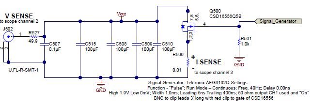
Figure 1 is an example of a power-supply output test setup where I monitored the response to a large step load on the output and also had the oscilloscope monitor the dynamic load current across a low-value resistor. I used a signal generator to drive the desired step load size with the desired rise and fall times and sensed voltage with a 50Ω cable attached to J502. The 50Ω R527 dampens any reflections on the cable. I used the tip-and-barrel approach to sense current across R500 with a 10x oscilloscope probe.

Figure 1: Test setup

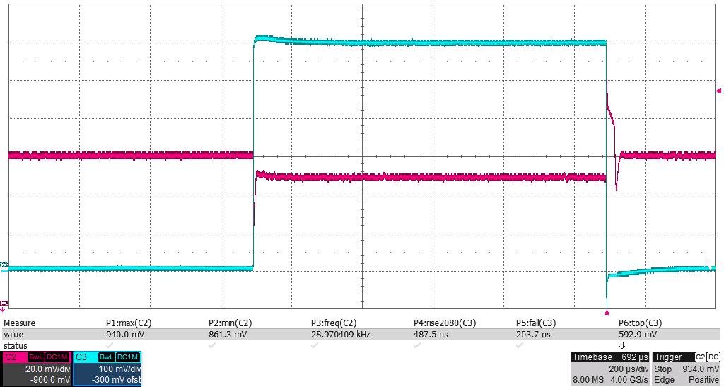
Figure 2 shows both the sensed voltage and sensed dynamic load current on the same oscilloscope when applying and removing a 59A pulse load.

The application requirements are that VOUT (the red trace on the oscilloscope/J502 in Figure 1) stays within a 855-945mV range under both load step and load dump. Dynamic current is measured across a 10mΩ resistor (R500 in Figure 1) tied to ground and is the green trace shown in Figure 2.

Figure 2: Step-load and load-dump response from 2A to 61A with dynamic current sense while connected to the oscilloscope

Based on Figure 2 and looking at the channel two red trace showing Vout, the voltage output drops to 861mV when applying the load step, then stabilizes at 889mV with the higher load. Upon removal (dump) of same added load, the voltage output peaks at 940mV before stabilizing at 900mV. Thus, the voltage output stays within the 855-945mV limits, and the test “passes.” Looking at the channel three green trace showing the voltage across the 10mΩ current sense resistor, the dynamic load goes from 0A to 593mV/10mΩ, or 59A and back to 0A.

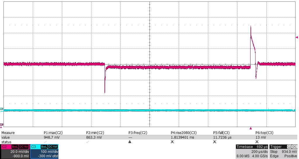
Disconnecting the current-sense probe from the oscilloscope shows a different voltage waveform on the output. See Figure 3.

Figure 3: Same dynamic response at VOUT with the current sense disconnected from the oscilloscope

Based on Figure 3 and looking at channel two red trace showing output voltage, the voltage output drops to 863mV when applying the load step, then stabilizes at 896mV with the higher load. Upon removal (dump) of the same added load, the voltage output peaks at 949mV before stabilizing at 900mV. Thus, the output goes above the 945mV limit and the test “fails.”

Off-site test experience

Testing with an off-board “load slammer” and trying to monitor both the output voltage on the main board and the dynamic load on the slammer made the dynamic response look very poor. When I removed the current-sense connection from the oscilloscope, I saw a good dynamic response. There, the current-monitor connection created a false fail.

If you are going to monitor both current and voltage on the same oscilloscope, you will need either an oscilloscope with fully isolated inputs or a dynamic load with sense resistor ground right at the voltage-ripple monitor. For the first option, you’ll also need two sets of differential probes with good input isolation.

Stay tuned for an upcoming blog highlighting a design with a dynamic load test interface which will allow monitoring both voltage and dynamic current at the same time without differential probes. 

Additional resources

Waveform audit: is your inductor saturated?

$
0
0

Inductors are key components in switched-mode power supplies (SMPSs). Inductor selection is an important design step in power-supply design, but can often pose challenges.  These challenges are generally eased by numerous design guides and tips, such as those given in the application sections of DC/DC converter data sheets. Such tools help designers select the right components for their application faster.

Choosing an inductor for your power supply includes considering many parameters like DC resistance (DCR), rated current and saturation current. Among these parameters, saturation current is one of the most interesting. Saturation current is generally defined in inductor data sheets as the DC current that will make the inductance decrease x% from its nominal value without current. This essentially means that when the DC current in the inductor reaches the saturation current value, the inductance value has decreased by a certain percentage (generally 30%). It implies that the saturation entry point is arbitrary and may vary from one manufacturer to another. In addition, depending on their core material, inductors will react differently when they reach saturation. There are two types of saturation behaviors:

  • Hard saturation: the inductance drops drastically as soon as the saturation point is reached (see Figure 1). This is the case for inductors with winding on a solid core.
  • Soft saturation: the inductance reduces progressively. This is the case for power inductors with winding on a powdered core.

When examining inductor saturation the inductance vs. current curve is preferable to the value of the saturation current.

Figure 1: Inductor core saturation: hard saturation (black) /soft saturation (red)

Now that you know what saturation current is and how it relates to the effective inductance value, how can you tell that an inductor is saturated?

One rapid way to determine this is to measure the current flowing into the inductor. In fact, when the inductor enters saturation the inductance drops, which means that the inductor current slope gets steeper. See Equation 1:

                 (1)

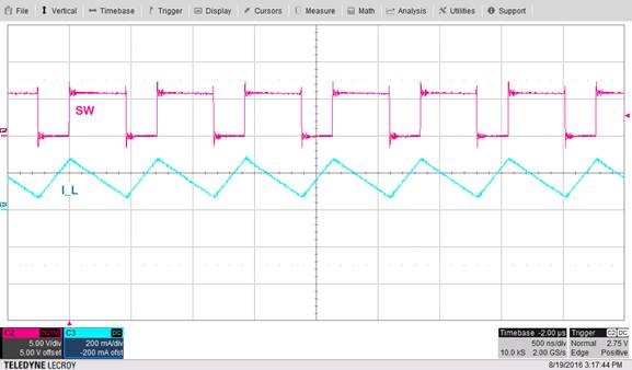
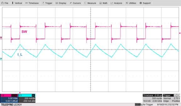
Figure 2 shows the inductor current waveform of a boost converter without saturation. In Figure 3, an inductor with a lower saturation entry point replaces the previous inductor. You can see that for the same DC current the inductor is saturated: the current rises sharply closer to the peaks.

Figure 2: Inductor current

Figure 3: Inductor current – saturation reached

Apart from the DC current that flows into the inductor, the ambient temperature also influences the saturation entry point. Inductor manufacturers specify the saturation current for the typical temperature in data sheets, and not considering this might lead to having the wrong inductor in your application. The inductance vs. current curve changes over temperature, as you can see in Figure 4. Therefore, the saturation current will vary as well with temperature and will be reduced for higher temperatures. 


Figure 4: The influence of temperature in saturation current

The importance of saturation current lies in the fact that saturation of the inductor for a DC/DC converter can lead to destructive consequences. When the inductor enters saturation, it can store less energy and the ripple current increases – meaning that the efficiency will be reduced. At this point, the inductor is behaving more like a resistor than an inductor. In addition to that, high current peaks will appear on the switch node because of the drop in inductance value occurring with saturation. This can damage the inductor itself or other components and create noise. Stability issues can result from the inductance decrease as well.

When selecting an inductor (after defining the parameter values), I recommend taking advantage of the tools available on inductor vendors’ websites, which enable you to compare inductors in the context of parameters such as saturation current, ambient temperature and total losses. Then, a rapid check in the lab of the inductor current under the actual operating conditions will surely help you determine whether the selected inductor is saturating or not. For more help on selecting an inductor for a buck converter application, please download our application note on selecting inductors for buck converters.

Additional resources:

USB chargers then and now: Type-C meets energy efficiency standards

$
0
0

While planning to write this post, I typed “type-C” into Google Trends. Interest in the term has been rising since 2015 shown in Figure 1.

Figure 1. Interest over time on Google Trends (Keywords: type-C)

USB Type-C devices are getting more and more popular in the real world as well, with many prevalent cell phones and tablets adopting USB Type-C. I expect products with USB Type-C to increase rapidly in the coming years.

Why 15 Watts (5V3A)?

Besides having a flippable plug that works regardless of orientation, USB Type-C delivers more power than any previous USB version. Although USB Type-C can support up to 100W for USB 3.1 and USB Power Delivery, system designers must choose features carefully to keep their overall costs reasonable.  The USB Type-C interface also introduces native power capability of 15W, which is six times the standard USB 2.0 charging rate. For most smartphones and tablets, 15W is probably adequate, with a reasonable cost. 

Diode Rectification and PSR are widely used for adapter current lower than 2A

In previous power adapters for mobile phones, a normal power level is 5V/2A or below. Primary-side regulation (PSR) is usually used for the AC/DC conversion because of its simplicity and ability to eliminate the optical isolator and programmable reference. A diode rectifier is used at this power level because the load current is not high. Figure 2 shows a simple PSR schematic with diode rectification.

Figure 2.Typical application circuit of UCC28704 with diode rectification

Synchronous rectification (SR) is preferable to PSR for 5V/3A adapters with design challenges

PSR saves costs because it eliminates the need for secondary-side feedback components and an optical coupler. However designing with PSR + SR is not as easy as using PSR only.

Most PSR controllers will detect the voltage of the auxiliary winding on the knee point when the secondary diode current goes to zero, as the voltage on auxiliary winding is the closest to VOUT/Na, where Na is the ratio of the auxiliary winding to the secondary winding.

There is a voltage bump on the auxiliary winding when the body diode conducts at the end of the secondary conduction time if using SR, refer to Figure 3. This bump will affect the PSR-detecting mechanism and cause stability problems, which may manifest as abnormal ripple.

Figure 3. Auxiliary Waveform Details

How to make PSR+SR stable

To stabilize PSR + SR, the UCC28704’s (PSR controller) datasheet makes it easier to work stably with SR drivers. tBW, tDMAG and working frequency are the parameters to design carefully. Where tBW is the SR bump width, tDMAG is the secondary rectifier conduction time

The critical parameter dictating the maximum switching frequency when using the UCC28704 with SR is determined based on tDMAG(min). The tDMAG(min) needs to be longer than 2.45μs, including the SR bump width (tBW) which is 750ns. The 750ns (tBW) is required for the internal circuit to filter out the SR bump change caused by MOSFET body-diode conduction sensed on the VS pin waveform. The corresponding switching frequency measured at the starting point of constant-current operation should not be greater than 55kHz.

A 5V/3A design with the UCC28704 (PSR controller) and UCC24636 (SR controller)

Following the guidelines, I made a 5V/3A board as shown in Figure 4. The ripple is below 150mV, and the efficiency curve is in Figure 5.

Figure 4. Universal AC Input to 5V/3A Ooutput Reference Design DOE6 and COC V5 Tier 2 Compliant TI Design Schematic

Figure 5. Efficiency Curves

The four-point average efficiency measured at a 150mΩ cable end with 115VAC and 230VAC inputs are 83.4% and 83.2%. The COC Tier 2 2016 compliance is 81.8% for full load and 72.5% for 10% load.

The board can meet the CoC Tier2 compliance with enough margins even with 150mΩ cable.

Summary

Following the guidelines in the UCC28704 data sheet, you can overcome the limitations and make a PSR + SR design that is low cost, yet has high-enough efficiency for USB Type-C adapters.

Additional Resources

SOIC-8 stands the test of time

$
0
0

As a millennial, it’s all about having the newest phones and gadgets, not to mention playing the newest games (Pokémon Go anyone?). But does newer always equal better? Personally, I’d rather stick with my bike than ride one of those hoverboards. Remember them? They were the hottest item of the 2015 holiday shopping season before people realized they had a slight issue with spontaneous combustion.

There are certain times in life where using a high-quality and reliable product or brand outweighs novelties and fads. A few things that come to mind: my car, my furniture and my grandmother’s peach cobbler recipe. Trust me. Nothing could ever improve upon that peach cobbler recipe.

Even the semiconductor world isn’t immune to trends and marketing hype. For example, in the world of direct current (DC)/DC regulator packaging, the focus is on creating the smallest package possible. However, semiconductor developers who focus solely on creating that smallest package possible seem to have forgotten one very important fact: there are tens of thousands of customers worldwide who still prefer traditional packages with pins or leaded packages, despite their larger size.

Don’t get me wrong: TI is also investing in cutting-edge package technologies. However, we haven’t forgotten our pin/leaded package-loving customers and so continue to release new products like the new SIMPLE SWITCHER® LMR23610/25/30 36VIN buck regulator family in trusted package technologies like small outline integrated circuit (SOIC)-8.

You may be curious as to why so many customers still like ancient packages like the 8-pin SOIC, or SOIC-8, when there are so many newer and smaller technologies available. Many customers prefer packages because they are easier to work with in the lab and the factory. The leads on SOIC-8 packages are very easy to hand-solder and work with on the bench. Designers can easily debug their circuits since the pins are exposed. In the factory, using a leaded package technology technology with pins enables designers to use visual inspection technology to confirm that the device has been soldered correctly and to screen out any faulty boards.

On the other hand, with a leadless package like a very thin small outline no-lead (WSON) or a quad flat no-lead (QFN), the pins are completely underneath the package, making it extremely difficult to solder or debug by hand. The location of the pins also makes visual inspection impossible, necessitating additional X-ray inspection equipment to confirm proper soldering connections.  Watch a video “Engineer It: How to Simplify the Power Supply Prototyping and Manufacturing” for a soldering demonstration on an SOIC-8 package.

(Please visit the site to view this video)

Additionally, the SOIC-8 on the LMR236xx family includes a single die attach pin (DAP) on the bottom to help extract the heat. This enables a lower junction-to-ambient thermal resistance (theta J/A) and better thermal performance than many QFN-style packages, like competitor A’s package in Figure 1.

 Figure 1: Thermal images taken at VIN = 12V, VOUT = 5A at 3A, 2MHz

For many customers, the easy-to-use aspects of a package with pins outweigh the size advantages of a leadless package. Whether you prefer to stay on the cutting edge of package technology or want peace of mind from using a trusted and reliable package, the SIMPLE SWITCHER regulator family has an option for you. Check our website for more information about the SIMPLE SWITCHER LMR23610/25/35 family.

Laying out an inverting buck-boost converter for success

$
0
0

It is common knowledge in the DC/DC converter domain that a buck converter or regulator integrated circuit (IC), such as the LM5017 family, can create a negative VOUT from a positive VIN. At first glance, the schematic of an inverting buck-boost converter using a buck regulator IC looks deceivingly similar to a buck converter (Figure 1a and 1c). But there are important differences in the two circuits, both in terms of voltage and current levels, switching-current flow, and layout.

I discussed the differences between VIN range, VOUT range and available output current IOUT max in an earlier blog post. The difference in layout arising from the difference in switching-current flow paths of an inverting buck-boost converter and a buck converter – although critical – is not as well understood.

Figure 1 illustrates the difference in switching-current flow in a buck converter and an inverting buck-boost converter. In the buck converter (Figure 1a and 1b), the input loop – comprising the input capacitor CIN, high-side switch QH and synchronous rectifier QL, carries high di/dt switching current. The output loop, comprising the synchronous rectifier QL, inductor L1 and output capacitor COUT, has a relatively continuous current. Thus, while optimizing the input-current loop area is critical, it’s not as important to optimize the output-current loop area.

Figure 1: Switching-current flow in a buck converter (a, b); and an inverting buck-boost converter (c, d)

The input- and output-current loops in an inverting buck-boost converter comprise the same elements as those in a buck converter (Figure 1c and 1d). The input loop has the input capacitor CIN, control FET QH and synchronous rectifier QL. The output-current loop consists of the synchronous rectifier QL, the filter inductor L1 and the output capacitor COUT. In an inverting buck-boost converter, however, both the input- and output-current loops carry high di/dt switching current because the filter inductor switches from CIN to COUT between the switching subintervals.

Because of the similarity in the buck and inverting schematics, the difference in switching-current paths often gets overlooked, and many inverting buck-boost designs and layouts are done just as they are for a buck converter, with only the input-current loop optimized for a small loop area. The buck to inverting buck-boost transition is often treated as a mere reconnection of VOUT and ground pins. But this approach fails to consider that the different current flows in a simple buck and an inverting buck-boost converter (using the same regulator IC) result in these issues:

  • The switching-current path shown in Figure 1c and 1d can have significant parasitic inductance, causing higher spikes on the switch node with these adverse consequences:
    • Higher electromagnetic interference (EMI) and noise as a result of switching current flowing through a non-optimized current loop.
    • In the inverting buck-boost configuration, the MOSFETs see a higher spike voltage on top of the |VIN + VOUT| voltage.
  • The switching current through the output capacitor has higher root mean square (RMS) (heating) content than in a buck converter for the same inductor current. The discontinuous current in the output capacitor also results in higher output ripple. Therefore, designers must keep these higher ripple currents in mind during output capacitor selection to satisfy both the VOUT ripple and IRMS current rating. Figure 2 compares the output capacitor ripple current in a buck and an inverting buck-boost converter. 

Figure 2: The ripple current in the output filter capacitor of a buck converter (a, b) is small, as the inductor is always connected to the output node. The ripple current in the output filter capacitor of an inverting buck-boost converter (c, d) is much higher due to the discontinuous nature of current flowing through the output capacitor.

Figure 3 shows how to optimize an inverting buck-boost power stage to achieve lower di/dt input and output loops. Figure 4 shows an example inverting buck-boost power-stage layout using the LM5017, a 100V synchronous buck regulator.

Figure 3: Optimization of power-stage components to minimize switching-current loop area (a) identifying current loops (b) minimizing current loops


Figure 4: An example layout of an inverting buck-boost converter based on the LM5017 synchronous buck regulator

Conclusion

Designers often use a buck regulator to create an inverting buck-boost regulator. But there are critical differences in the switching-current flow between buck and inverting buck-boost circuits. In particular, designers should pay attention to output filter capacitor selection and the switching-current loop layout to achieve the best reliability and noise performance.

Additional Resources

The difference between hysteretic-mode converters and traditional regulators

$
0
0

When designing a power circuit, many of the selections available on the market, such as traditional voltage and current-mode regulators, look similar. You know it will do a certain job - for example, step-down DC/DC conversion - but you may not know how the many choices compare to each other.

If you haven’t considered it before today, my recommendation is a hysteretic-mode converter.
Hysteretic-mode converters are branded in many different ways, including D-CAP™, D-CAP+™, D-CAP2™, D-CAP3™, constant-on-time, or DCS-Control.

When you’re deciding between the many choices, you probably do what I do; search online and find a comparison report, or find a site with reviews to see recommendations and complaints.

To help you in this effort, I authored a 3-part series of articles “Hysteretic-Mode Converters Demystified” aimed at comparing a hysteretic-mode step-down switching regulator with traditional voltage-mode and current-mode regulators. This series in Power Electronics Technology magazine is based on lots of measurement data behind the scenes (see example in Figure 1) and includes unbiased comparisons as much as possible. 

Figure 1. Screenshot of the many measurement plots I compiled for the comparison.

I kick off part 1 of the article series “Hysteretic-Mode Converters Demystified” by reviewing basic operation differences of hysteretic-mode, voltage-mode and current-mode converters. This part illustrates the fundamental differences and also points out similarity of converters.

In part 2 “Voltage and Current Mode Control,” I compare large signal load and line transient behavior. This section reviews the many technical plots pictured above to highlight the differences between control modes.

In part 3 “Regulator Stability,” I examine small signal behavior and stability.  This part reviews three different small signal measurements (Bode plot, output impedance and small signal load transient) so you can get good idea of how hysteretic-mode converters perform.

I hope you enjoy the article series and I look forward to answering any questions you may have. If you are a more visual learner, view the seven-part video series based on these articles “Fixed Frequency vs Constant On-Time Control of DC/DC Converters”.

Additional resources:


Why should you count squares?

$
0
0

When I studied electrical engineering at the university, math was extremely important. My math professor was so diligent that he would attend other classes to see if the lessons involved math that he needed to teach us to make our lives easier. More than once he changed his lesson plans to incorporate math topics from the other classes, so I was very grateful that he was so passionate.

When I became an application engineer for power supplies, I quickly learned that there are parasitics in all components. The formulas to calculate the best-fitting component became more and more complicated when including these parasitics. Sometimes a simplified formula or even a rule of thumb helped me get at least close to a result, enabling me to find the best-fitting available component through trial and error.

One issue where I could never use math, however, was when deciding about the best layout. I still don’t have a really good simulation tool that can predict exactly which layout is the best fit for the specific power supply I want to design. My dilemma gets even worse if the IC includes several converters, like LCD (Liquid Crystal Display) or OLED (Organic Light Emmiting Diode) display power products. The parasitics of a layout not shown in the schematic do influence the performance of a circuit and can even cause hazardous failures in a power supply. So it is important to do the layo=ut right the first time.

One parasitic effect to keep in mind when doing a layout is the trace or plane resistance. Here is a rule of thumb that I’ve learned to estimate it:count squares.

I learned about this rule the first time I laid out a power-supply design. I remember being somewhat puzzled because I could not believe that it could be so simple, but it is; I even can use math to show you that it’s true.

Equation 1 calculates the resistance of copper:

                            (1)

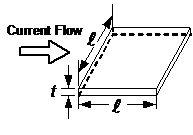
Figure 1 shows a piece of copper on top of a printed circuit board (PCB).

Figure 1: Copper piece carrying current in a power-supply design

Assume the current is flowing from left to right along l  and distributes evenly in area A. In this case, Equation 1 becomes Equation 2:

                            (2)

You can see now that the resistance of this piece of copper is independent of the dimension l  . So now the formula for resistance on a PCB changes to Equation 3:

                 (3)

Where ρ is the well-known specific copper resistance and the production specification of the PCB defines the thickness of the copper.

This means that regardless of how big l  is, the resistance stays the same. For a layout person this is really good to know, because if you want to make the resistance as small as possible, make it as wide and as short as possible.

You can determine the thickness of copper on a PCB from the requested production parameter (see Table 1) and estimate the resistance of a specific piece of copper in the layout by counting squares.


Table 1: Copper Thickness and resistance based on the production parameter Copper Weight
 

Assume your piece of wire looks like Figure 2.


Figure 2

Divide it into squares, as shown in Figure 3.


Figure 3


Say that you can fit 10 squares into your piece of wire, like in Figure 3. If you are using 1oz copper on your PCB, the resistance of this piece of wire is roughly 5mΩ. If a current of 1A is going through this piece of wire, the voltage drop from one end to the other end will be 5mV. Assuming a voltage of 1V on one end, the voltage on the other end is 0.5% smaller – and this is just one piece of wire. Double the width of your wire and you halve the resistance.

So even if it is relatively easy to calculate the parasitic resistance, using my eyes and estimating the number of squares that fit into the wire made it a lot easier for me. Let me know how this works for you in the comments below!Check out the LCD/OLED display bias solutions offered by TI and share your results in the LCD/OLED Display Bias Solutions forum on the TI E2E™ Community.


USB Type-C: charging a new world

$
0
0

USB Type-C™ is upon us, representing the most significant change to USB that most consumers will notice to date. On top of a new reversible connector, the maximum power has increased to 15W. Higher wattage makes it difficult to design power adapters that meet the required efficiency and standby power standards while maintaining the small form factor that customers expect. But it is not impossible, since new flyback controllers such as the UCC28704, which TI released earlier this year, further improve performance and include many advanced features for USB Type-C chargers.

CCUV

All short-circuit protection is not equal. While most controllers protect against hard short-circuit events, where the output current attempts to run far away from the set limit, they do not protect against soft short-circuit failures. When dust or other foreign objects get into the small USB connector and short across the power leads, the connector bypassing current charging path, so-called the soft short-circuit occurs, causing the converter to operate in faulty pathed over-load current that overheats then damages the USB connector in soft short-circuit. Constant Current Output Under Voltage (CCUV) shutdown provides soft short-circuit fault detection and protection to prevent damaging the USB connector. CCUV operation and characteristics are illustrated in Figures 1 and 2.

Figure 1: Soft-short protection


Figure 2: Output V -1 Curves

Efficiency boost

The Department of Energy (DoE) Level VI (mandated) and European Union Code of Conduct (CoC) V5 Tier 2 standards set up the efficiency and standby power consumption levels for USB Type-C chargers.

To meet and exceed these standards, the UCC28704 has these enhancements:

  • An increased maximum demagnetizing time ratio (Dmag) to 0.475. This increase mainly helps reduce secondary-side peak current and RMS current for the same rated output current to boost efficiency. This helps to achieve higher efficiency at heavy (75%) and full (100%) loads.
  • Two techniques boost efficiency at 10%, 25% and 50% loads:
    • Enabling light to medium load-switching frequency at about 25kHz to reduce switching losses while avoiding audible noise.
    • The introduction of a “wait” state to shut off internal unused circuits, thus reducing the device’s bias energy at light to medium loads.

As Table 1 shows, the UCC28704 in TI Designs Universal AC Input to 5V 3A Output Reference Design DOE VI and CoC V5 Tier 2 2016 Compliant (PMP15002) can meet these standards with a 150mΩ cable, while passing both conducted and radiated electromagnetic interference (EMI) while not sacrificing size or cost. These benefits are not limited to 15W, and as TI Designs Universal AC Input to 5V 2A Output Reference Design CoC Tier 2 2016 Compliant (PMP11612) shows, the UCC28704 can achieve the same high performance at 10W as well. By enabling such high efficiency, the latter reference design meets DoE Level VI and CoC V5 Tier 2 efficiency with a diode on the output, enabling a very low-cost solution, which reducing  the cost from where an SR MOSFET with driver device has to be used in alternative solutions.


Table 1: TI’s PMP11612 and PMP15002 reference designs exceed mandated DoE and CoC levels (efficiency is the average value of four-point efficiency at 25%, 50%, 75% and 100% loads)

Besides the reference designs, other design tools available on the UCC28704 product page include a SPICE model, WEBENCH® Designer calculator, Excel calculator, MathCAD calculator, UCC28704EVM-724 evaluation module and a user’s guide.

Power Tips: Where to connect frequency analyzer reference leads for Bode plot measurement – Part 1

$
0
0

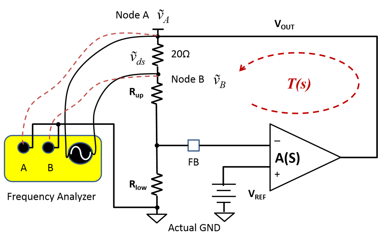
Whenever a system incorporates a negative feedback loop, the loop gain, T, becomes an important performance parameter to measure and optimize for stability, output regulation and transient-response performance. Voltage injection is a widely adopted method for measuring T. Figure 1 shows a typical voltage-injection T measurement setup. The feedback path is cut off between VOUT and Rup. A disturbance voltage is inserted. All signals refer to ground.

Figure 1: Typical T measurement setup

Equation 1 measures T as:

                           (1)                 


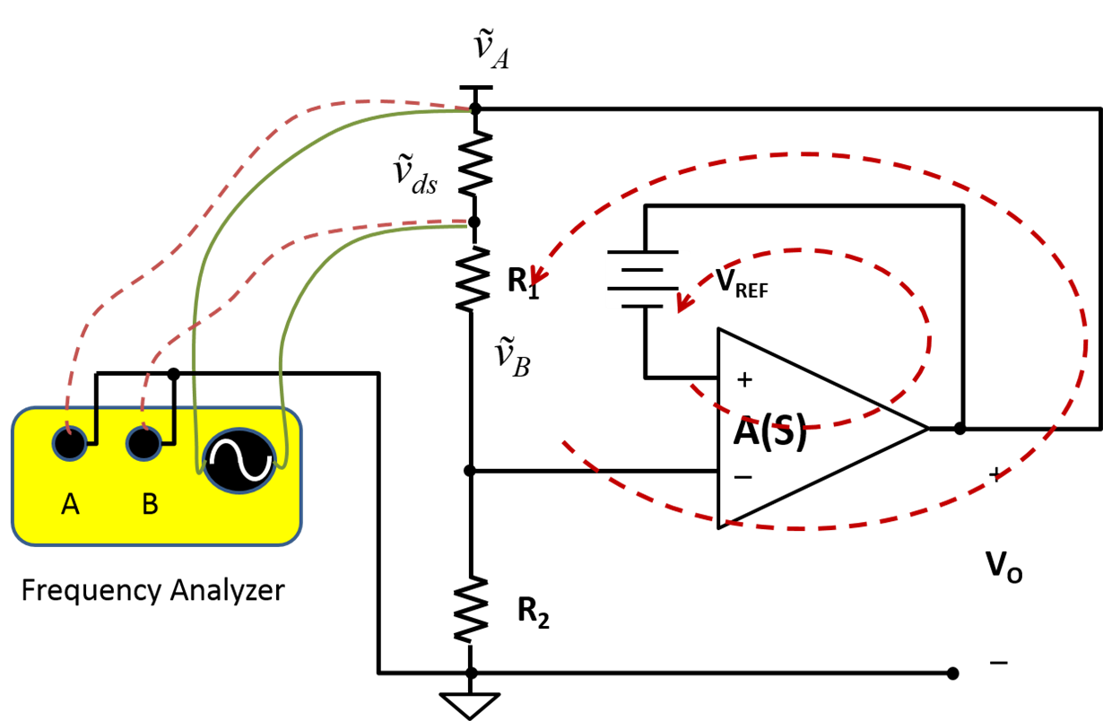
Signal receivers A and B have two leads which provide a reference point for signals A and B, respectively. Figure 2 shows the leads.

Figure 2: Probes of receivers A and B with their reference leads

In most cases, these leads connect to ground, and because of that, they are called GND leads. But is that always the case? To answer that question, I will demonstrate an example using the LM4041-N, a precision shunt voltage reference. Figure 3 shows a typical application circuit for the LM4041-N.

Figure 3: LM4041-N typical application circuit

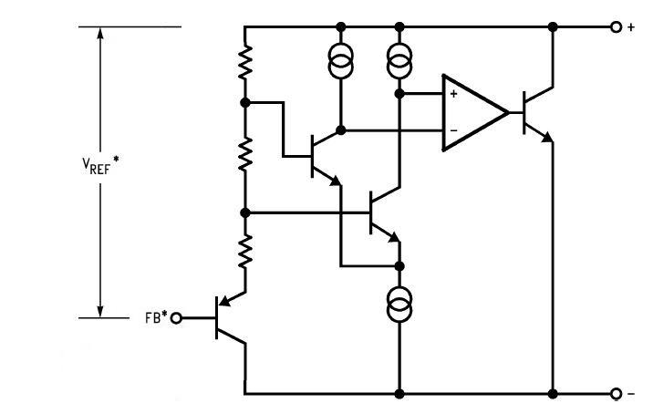
The LM4041-N keeps the voltage across VO to the FB pin at 1.24V, as Figure 4 shows. The resistor divider sets the output DC voltage. RS provides current for the LM4041-N and load.

Figure 4: LM4041-N block diagram

To generate a 2.5V reference from a 12V bus, I used these components:

  • R1 = 10kΩ.
  • R2 = 10kΩ.
  • RS = 10kΩ.
  • Co = 0.22µF.

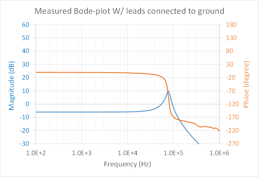
Figure 5 shows the Bode plot measurement result using the setup shown in Figure 1. The result does not correspond to tight DC regulation, as I expected. Nor does it provide a direct indication of stability.

Figure 5: Measured Bode plot with reference leads connected to ground

I derived the AC small-signal models referring to ground. Figure 6 shows the model.

Figure 6: Small-signal model referring to ground

 With the reference leads connected to ground, the break point between Vo and R1 only cutting off part of the feedback path. I examined the LM4041-N block diagram. The positive input of the gain stage connects to Vo from the AC perspective. By moving the reference leads to Vo, I now can break the feedback loop completely between R2 and ground. At this break point, looking backward is the regulator output, RS and Co in parallel. R2 is the impedance looking forward. For most frequencies, the impedance of Co is much smaller than R2. Figure 7 shows the small-signal model referring to Vo.

Figure 7: Small-signal model referring to the output

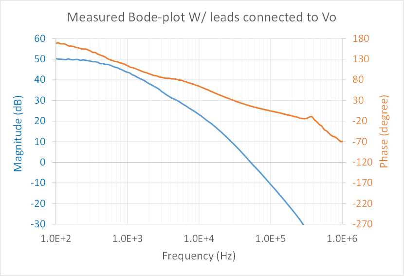
Figure 8 shows the measurement results using the setup shown in Figure 7.

Figure 8: Measured Bode plot with reference leads connected to Vo

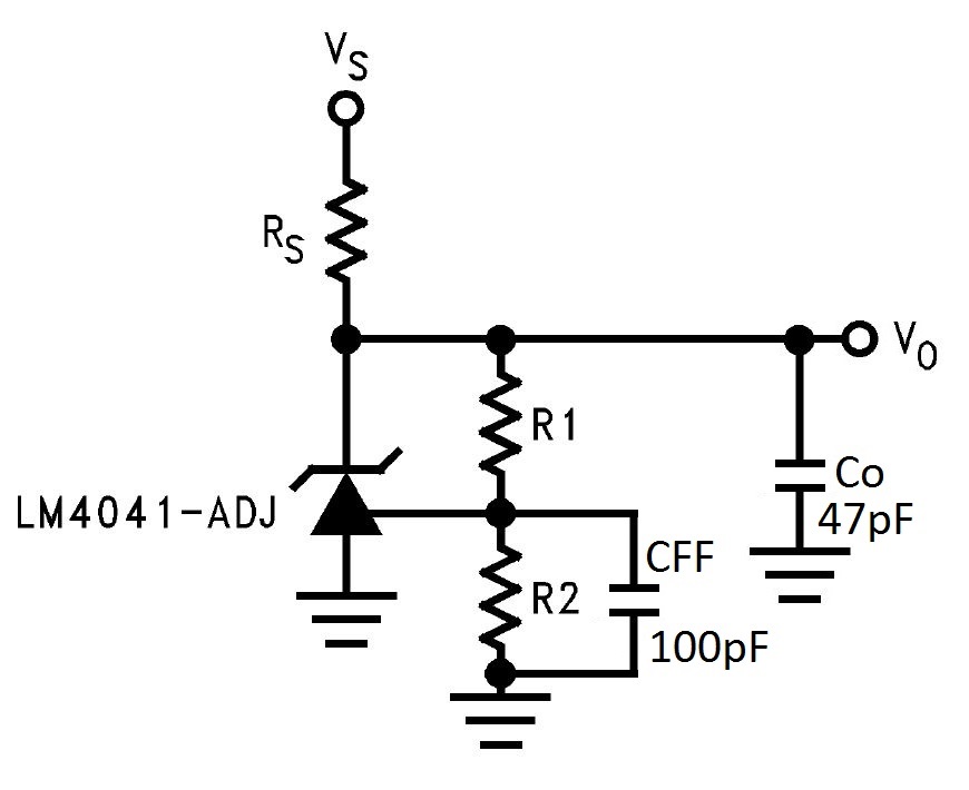
The result shown in Figure 8 indicates that the stability needs improving. I reduced the output capacitor from 0.22µF to 47nF and added a phase-boosting capacitor in parallel to R2, as shown in Figure 9.

Figure 9: Final schematic of LM4041-N as a 2.5V voltage reference

Figure 10 shows the improvement with the reduced Co and phase-boost capacitor, Cff. With the changes, phase margin has increased from 16 degree to 45 degree.


Figure 10: Measured Bode plot with a different Co and Cff

You can use the LM4041-N to show how to find a point to connect the reference leads of a frequency analyzer for Bode plot measurement. First, develop an AC small-signal model. Then, identify a reference point so you can find a break point to meet both of these requirements:

  • All feedback paths are cut off at the break point.
  • The impedance of the break point looking backward is much smaller than the impedance looking forward.

Additional resources

Is integrated GaN changing the conventional wisdom?

$
0
0

As a power electronics engineer, there is a saying that no success is made without the lessons learned from power devices blowing up. This seemed true during my years of experience debugging switched-mode power supplies with silicon-based MOSFETs. It is through trial and error and the study of device failures that you learn how to design a converter that works reliably.

In the early stages of gallium nitride (GaN) power FETs, failures were common. More stringent gate-loop design requirements, much higher dv/dt and the effect of common-source inductance all made the circuit much more sensitive to parasitics and noise. When TI’s first 600V GaN power stage samples came out, I marveled at the product’s robustness and the effectiveness of its self-protection functions. Even though the power stage had been validated through rigorous testing, my previous experience with silicon parts left me curious of its robustness under actual usage. More importantly, will these functions change the conventional wisdom of circuit prototyping and debugging ?

In a recent design of an interleaved converter, I used two TI half-bridge LMG3410-HB-EVM evaluation modules (EVMs) with some basic DC bus design, controlled by a UCD3138 digital pulse-width modulation (PWM) controller. When the two interleaved half bridges worked together, I saw that the PWM signal was repeatedly affected by high dv/dt (100V/ns), causing shoot-through across the FETs at 480V and triggering the integrated overcurrent protection (Figure 1).

Unlike the majority of FETs – which would fail in this situation – the LMG3410 integrated power stage enabled me to repeat the fault condition without damage, and to debug to the root cause quickly. This would have been very painstaking and possibly unsafe to do with traditional parts.

Figure 1: Self-shutdown of the power stage following a shoot-though event (blue: upper-FET PWM; yellow: lower-FET PWM; green: inductor current)

By varying the slew rate through RDRV, I found that 50V/ns or 100V/ns with single-phase operation had robust operation, while 100V/ns with two-phase operation did not. The root causes were contamination from common-mode (CM) noise and a nonoptimized layout of the controller’s peripheral circuits, resulting in a clock-synchronization mismatch across different PWM channels (Figure 2).

Figure 2: PWM out-of-sync leads to inductor current surge (blue: upper-FET PWM; yellow: lower-FET PWM; green: inductor current; red: fault-signal triggering)

TI’s ISO7831 digital signal isolator provides an adequately high CM transient immunity (CMTI) rate (>100V/ns), but the isolated power supply (which usually has much higher CM capacitance) would easily couple noise from the switching-node voltage to the control-side ground at high dv/dt (Figure 3). With multiple phases operating simultaneously, more CM noise would be injected into the control side.

Power-supply designers sometimes overlook this issue, since silicon devices and some GaN FETs with external drivers will not achieve such a high slew rate. I successfully resolved the issue by adding extra CM chokes on the upper FET’s isolated power supply and improving the decoupling loop of the digital controller, which reduced ground bouncing and noise coupling at the controller. Thanks to LMG3410’s integrated protection functions, I didn’t experience a single catastrophic failure during the whole debugging experience, despite repeated CM noise-induced faults.

Figure 3: CM capacitance across isolated power supply and digital isolator

Besides overcurrent faults, overtemperature events are common occurrences in power converters. Although an experienced engineer has good thermal design skills, keeping the device junction cool is still challenging, and there is not much margin for error. Over time, events such as fan failures or heatsink deterioration can cause catastrophic failures. Fortunately, the LMG3410 has integrated overtemperature protection, and it came to my rescue when my fan’s power supply got turned off accidentally. The thermal trip point is set at 165°C, allowing enough margin for brief temperature excursions but preventing the device from suffering permanent damage due to cooling-related system failures.

While GaN brings advantages in system efficiency, size and cooling, its high switching speed and frequency also present increasing challenges. The protection and other integrated functions of TI GaN products are changing the conventional wisdom of using discrete Si MOSFETs for us to learn about the intricacies of high-speed switching-converter designs. These products not only protect the device against permanent damage as we debug our new designs, but also improve robustness by preventing gate overstress under long-term operation, since an integrated driver design reduces gate ringing.

The world has seen tremendous scaling of electronics and improvement of system density with Moore’s law. This trend is now coming to power electronics, thanks to the development of GaN technology and the introduction of easy-to-use GaN power stages like the LMG3410 with self-protection features. 

Get to know TI’s GaN solutions.

Additional Resources:

Learn more about GaN reliability: 

How to design a limited power source industrial AC/DC power supply with minimal components – part 1

$
0
0

DIN rail power supplies in industrial equipment.

In this two-part series, I’ll explain the basic details of limited power source (LPS) requirements and how you can optimize the feedback loop with the UCC28740 primary-side regulated (PSR) flyback controller to reduce the overall components in high-power-density industrial DIN rail power supplies.

Increasingly, the responsibilities of a power-supply designer extend beyond merely meeting a product’s functional specifications. The latest-generation products need to be robust and safe over various operating conditions such as overcurrent, overvoltage, short circuit and limited power output.

To meet safety requirements for equipment powered using industrial power supplies, it is important to precisely limit current and power during all operating circumstances, which include normal conditions, load-transient conditions and severe output-fault conditions. In addition, the voltage should exceed certain limits to prevent electrical shocks for the end user. Limiting power, current and voltage also has a multitude of associated benefits, which include reduced wire gauges for output interconnections, reduced component stress for downstream converters, reduced system cost and increased system reliability.

Safety standards such as IEC - International Electrotechnical Commission IEC 60950-1 and the National Electrical Code (NEC) define these limits for voltage, current and power.

For instance, IEC 60950-1 covers LPS requirements of power supplies in Clause 2.5 of the standard, shown in Table 1. Table 2B of IEC 60950-1 Clause 2.5 elucidates the restrictions for power sources for current and apparent power for cases where you do not use external overcurrent protection such as inherently limited source.

Table 1: IEC60950 limits for power sources without an overcurrent protection device

Figure 1 is a graphical representation of Table 1.

Figure 1: Graphical view of UL60950 limited power circuits

Similarly, the NEC also sets guidelines for maximum possible voltage, current and power to govern the installation of wiring and equipment in commercial buildings and residential areas.

In the next installment of this series, I’ll explain the protection implementation with minimal components.

Additional resources:

  • Explore these industrial power-supply designs:

Thermal good – quite a hot topic

$
0
0

Looking back on DC/DC power supplies, the power-good (PG) function has been well-known for many years. The PG pin is an open-drain output that requires a pull-up resistor connected to the output voltage or any other system voltage. It is used in many applications to indicate whether the output voltage has reached an appropriate level or not. When the DC/DC converter reaches the right output-voltage level, the PG pin goes into a high impedance state and the signal goes high. The PG signal can  monitor the correct output voltage or for the startup sequencing of multiple rails. Figure 1 shows a typical waveform of PG functionality during startup, operation and shutdown of the IC.

Figure 1: PG operation in the TPS62480

Besides the well-known PG feature, there is a new function available called thermal good (TG). The TG pin is also an open-drain output, like the PG, that requires a pull-up resistor. While the PG signal depends on the device’s output voltage, the TG signal depends on IC temperature. As long as the junction temperature is below the TG threshold temperature, the logic level at the TG pin is high. If the junction temperature exceeds that temperature, the TG pin goes low.

With TG, the system can take action to prevent excessive heating or even thermal shutdown. For example, if the temperature increases due to intense power demand from a processor and the TG signal goes low, a host MCU can reduce the operating frequency of the processor, which will draw less current and thus less heating, increasing power-supply reliability and preventing thermal shutdown.

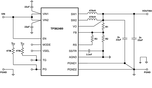
Figure 2 shows a typical application schematic of the TPS62480, a 5V, 6A dual-phase step-down converter that implements this new TG function.

Figure 2: TPS62480 typical application schematic (PG and TG pulled up to VOUT)

For this device, the TG threshold temperature is typically 120°C with a hysteresis of 10°C. So when the IC temperature is below 120°C, the logic level at the TG pin is high. The thermal shutdown temperature is 160°C with 10°C hysteresis for this IC. Because the recommended operating conditions limit the junction temperature to 125°C, the TG output can ensure that the device is always operating within the recommended junction temperature.

Figure 3 demonstrates the operation of the TG function. It’s based on the typical application circuit of Figure 2, where the TG pin pulls up to the TPS62480’s output voltage. An example rising and falling temperature profile shows the TG function as well as the thermal shutdown.

Figure 3: TG behavior

Besides the TG and PG features, the TPS62480 provides a voltage select (VSEL) pin to easily adjust the output voltage between two levels and comes in a quad-flat no-lead (QFN)-style, easy-to-assemble HotRod™ package.

When do you start using the thermal good feature to increase system reliability?

Additional resources

Understanding Voltage References: Simple Current Sink

$
0
0

As discussed in the previous posts in this voltage reference series, generating DC currents of arbitrary magnitude is a simple and straightforward process using operational amplifier feedback and a voltage reference. To this point, we have addressed several external opamp architectures for realizing individual or networks of current sources and sinks. In this final installment of the series, we will address an architecture which utilizes feedback from within the voltage reference itself. Let’s begin by considering the voltage reference’s symbol and its actual functional block diagram as displayed in Figure 1 below.

 Figure 1: Voltage Reference and its Functional Block Diagram

We have borrowed the symbol for the Zener diode because that’s essentially how the voltage reference behaves; however, this behavior is achieved through clever design rather than simple device physics alone. Consider the self-referenced (cathode-reference-tied) configuration that was utilized in previous posts and shown in Figure 2 below.

Figure 2:  Voltage Reference Typical Operation

So, what can we say about this set up? First of all, we can greatly simplify and define the situation with all the currents in Figure 2 as shown in Equation 1.

That is, IBIAS is the summation of the opamp quiescent current, IQ, and the emitter current, iE, of the bipolar junction transistor (BJT). Equation 2 further simplifies this by acknowledging that the opamp quiescent current will be negligible compared to the emitter current during normal operation.

Equations 3 and 4 define the emitter current beginning with the diode equation for the base-emitter junction and assuming forward bias operation with nominal ideality factor.

As indicated by Equation 4 above, there must be some base-emitter voltage present to maintain IBIAS. This of course implies that there is a non-zero difference between vref and VREF in Figure 2; we will account for this by defining vref in Equation 5 in terms of VREF and a small perturbation voltage, εv.

We can now define εv in terms of the base-emitter voltage and opamp gain as shown in Equations 6 and 7.

Clearly εv drops to zero in the ideal opamp case; however, let’s consider some very conservative values. Equation 8 below solves Equation 7 assuming the vBE required to maintain IBIAS is 0.5V and the gain of the opamp is a mediocre 104.

For a 1.25V voltage reference, this represents an error of some four thousandths of a percent or 40ppm—that is, such an error can be safely regarded as negligible. 

Now consider what happens to εv when we increase the input voltage, and therefore IBIAS; specifically, suppose we double IBIAS from some arbitrary operating point as illustrated by Equations 9 and 10.

The change in VBE required to support doubling IBIAS can now be derived by dividing Equation 10 by Equation 9 and simplifying terms as follows in Equations 11 through 13.

Finally, we can derive an equation for the change in εv required to support doubling IBIAS as shown in Equations 14 and 15.  

Substituting in the room temperature value of the thermal voltage, VT, and assuming (again) the mediocre opamp gain of 104 we can solve Equation 15 for a conservative value of Δεv required for doubling IBIAS, resulting in Equation 16 below.

In this case, every time IBIAS is doubled the voltage at vref increases by only 1.792μV. It is this multiplication of opamp gain with the exponential IV characteristic of the base-emitter diode which mimics Zener breakdown behavior.

Connecting the voltage reference differently we can leverage its internal opamp to generate a simple current sink as shown in Figure 3 below.

Figure 3:  Simple Voltage Reference Derived Current Sink

To visualize what’s going on here, consider the functional diagram inserted in place of the symbol as shown in Figure 4 below.

Figure 4:  Simple Current Sink Functional Diagram

Notice that the VIN, RBIAS, and BJT circuit essentially acts as an inverting output stage for the opamp. Therefore, we can collapse the total combination into a new opamp symbol with a new gain, AT, and reversed input polarity as shown below in Figure 5.

Figure 5:  Simple Current Sink Functional Diagram and Equivalent Circuit

Thus, we have arrived at the same current sink circuit discussed in the first post in this series.

Throughout this series we have investigated the important topic of generating current references from voltage references. The first post covers precision, single sources and sinks of arbitrary magnitude (which can, of course, be used to implement bias networks); the second and third posts discuss a method by which bias networks might be derived with a single feedback device if a tradeoff of precision and component count is workable; and finally, this post discusses a greatly simplified method of implementing the current sink (specifically) discussed in the first post. The architectures discussed throughout this series are a handy addition to any design toolbox, and Texas Instruments has a wide variety of voltage references which can be used to realize these designs.

Selecting voltage detectors, supervisors, and reset ICs for system safety: part 1

$
0
0

Power-supply voltages in telecom, industrial and avionics applications can vary for many reasons, such as line and load transients; power outages; or a low battery. Voltage detectors and supervisors/reset integrated circuits (ICs) provide an early indication of supply-voltage deviations related to these issues to help protect the system.

Although voltage detectors and supervisors/reset ICs have the same functionality, they are used in different types of systems. A voltage detector monitors a voltage (like a battery voltage) and indicates to users that the voltage is low. Voltage detectors usually don’t have a delay, but they do have built-in hysteresis to prevent false triggers if the voltage is hovering around the threshold voltage.

A supervisor/reset IC monitors a supply voltage and resets or turns off another device like a microprocessor if the supply voltage is low. These devices usually have a programmable output delay to prevent the system from returning from reset before the supply voltage is stable.

Voltage detectors and supervisors/reset ICs have different features and parameters, making it tough to choose the right one for a given application. The key to choosing a voltage supervisor is to know the features you need and then select one based on your desired size, package type and price. In the first installment of this two-part series, I will discuss the simplest voltage detectors and some different output options. In the second installment, I’ll cover advanced monitoring and various features in voltage detectors and supervisors.

The simplest way to monitor voltage

For some applications, you may only want a basic, small and easy-to-implement voltage detector or supervisor/reset IC. These devices provide a low output voltage or reset signal when the supply voltage drops below the factory-programmed reset threshold. The output signal remains active for a fixed time after the supply voltage rises above that threshold. The available threshold options vary by part. Typical values include 2.63V, 2.93V, 3.0V, 3.08V, 4.38V and 4.63V. Accuracy also varies; while usually around 3%, it can be as precise as 0.75% overtemperature for some devices.

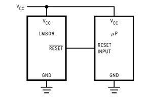
Basic voltage detectors or reset ICs don’t require any external components (except for maybe a pull-up resistor at the output) and are available in small, three-pin packages. Figure 1 shows an example of a simple voltage supervisor, the TI LM809.

Figure 1: LM809 typical application circuit

When the supply voltage at VCC drops below the LM809’s reset threshold, the reset pin drops low and triggers the microprocessor to reset.

Output type: active low vs. active high, push-pull vs. open drain

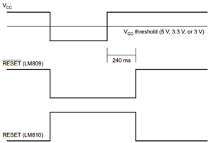
Active low and active high refer to a reset type. Active-low reset starts high; when the supply voltage drops below the voltage reset threshold, the reset pin goes low. Active-high reset is the exact opposite. The reset starts low, and when the supply voltage drops below the voltage reset threshold, the reset pin goes high. See the application curve in Figure 2.

Figure 2: Active low (LM809) vs. active high (LM810)

Push-pull and open drain refer to an output type. Push-pull uses two transistors at the output, with the top transistor turning on to set the output high and the bottom transistor turning on to set the output low. Open drain uses one transistor to set the output low and a pull-up resistor instead of a top transistor to set the output high. The advantage of push-pull is speed and lower power consumption. Open-drain outputs, however, can be wired together to create an OR/AND logic output configuration. Figure 3 illustrates both open-drain and push-pull outputs.

Figure 3: Output types

Now that I’ve covered the basics of voltage detectors and supervisors/reset ICs, stay tuned for part 2 to see various features and more complex ways to monitor voltage.


Keeping DC/DC solutions (super) simple for cost-sensitive applications

$
0
0

Keeping DC/DC solutions (super) simple for cost-sensitive applications

Have you recently upgraded your TV to one with a larger screen and ultra-high-definition resolution? Have you installed a new set-top box with six-channel simultaneous digital video recording? Does your modem enable 200Mbps Wi-Fi speeds? Can you control your home air-conditioning unit or car ignition with your smartphone?

Technology is indeed moving very fast, and behind the curtain, continuous innovation toward better performance, novel features and sleeker designs are the foundation behind the development of next-generation consumer devices.

For example, I have been amazed with the new generation of digital TVs and how the major brands continue to release models with higher image resolutions, sleeker designs and bigger screen sizes. They are now talking about 8K HD by 2020. On top of that, the leading manufacturers have dropped pricing significantly over the past 10 years, despite improving features and performance over previous models.

This is also true for DC/DC power solutions for consumer electronics. There is a demand for technology and innovation. And new DC/DC solutions like the TPS562201, TPS563201 and TPS564201 are smaller and simpler, but have higher efficiency to reduce power consumption and meet market needs.

Better efficiency

Through a recent advancement in package technology called flip-chip on lead (FCOL), TI can now manufacture DC/DC converters without wire bonding. The die connects directly to the lead frame through copper bumps, which reduces the on-resistance of the MOSFET (Rdson), resulting in higher efficiency and lower power consumption.

While wire bonding for conventional packages typically requires more space due to the height and length of the wires, with FCOL the copper bumps are located beneath the die and do not require additional space, thus enabling smaller overall package sizes. See figures 1 and 2. The TPS56x201 series implements FCOL package technology.

Figure 1: Flip-chip on lead (FCOL) compared to conventional wire bonding

For better light-load operation, the TPS56x201 family of DC/DC solutions also has much lower standby quiescent current (Iq) and implements TI’s advanced Eco-mode™ for high light-load efficiency, making it easier for designers to meet low- power standby  requirements from regulatory bodies like Energy Star and the Energy-Using Products (EuP) directive. For example, a device with a 12V to 5V conversion at 40mA would be able to support 90% efficiency. Refer to figure 2 for 3A TPS563201 and 4A TPS564201 efficiency curves.

Figure 2: TPS563201 and TPS564201 efficiency curves

Smaller PCB size

The earlier-generation TPS54326 device has been popular in consumer applications. This device is offered in a simple small-outline integrated circuit (SOIC) eight-pin package and uses TI’s DCAP2™ control scheme, which provides fast transient response without the need for external phase-compensation components.

As a next-generation solution, the TPS563201 offers a much smaller small-outline transistor (SOT)23 six-pin package – three times smaller than the previous solution. The new solution also requires fewer external components and features a fixed 1ms soft-start time, which eliminates the need for an additional capacitor for soft-start time adjustment (see figure 3). You also won’t need a voltage regulator capacitor for internal low-dropout regulator (LDO) operation.

Figure 3: TPS54326 external components compared to TPS563201

Easy to design

Aside for the fact that the TPS56x201 series of devices (refer to table 1) provide the lowest external components count with very good efficiency and very fast load transient response, the devices are also easy to use for different sockets needing a DC/DC buck converter on the board. This flexibility is due to pin-to-pin compatible between all devices and the ease with which to switch the devices on the board with minimal changes even if the load current requirement changes up to 4A. The TPS56x201 series also provides very good light load efficiency with an advanced Eco-mode™ feature to support power consumption regulation during stand-by mode.  And if this is not needed and operation at light load is preferred to be running in constant switching frequency, the TPS56x208 series would be able to cover this need as well.  Refer to table 1 below.

Table 1:  TPS56x201 and TPS56x208 pin-to-pin compatible device family

Other cost-sensitive applications

Given the new devices’ ability to support simple, cost-effective and smaller solutions in consumer applications, we are also seeing the TPS56x201 implemented into Bluetooth® speakers, multifunction printers, game consoles, enterprise computing and drones. The TPS56x201 and TPS56x208 provide simple and high-efficiency solutions for 5V, 12V and 15V VIN bus rails for currents as high as 4A.  With the high rate of adoption for these solutions in DTV and other consumer applications like set-top-box and modems, these solutions will provide a lot of value to various end-equipment applications where efficiency, ease of use, smaller size and over-all system cost are key factors.  See TI’s portfolio of DC/DC buck converter solutions in www.ti.com/dcdc.

Before digital control, there were general-purpose PWMs

$
0
0

For those of you who don’t know me, let me get the formalities out of the way. I absolutely love digital control! You know, stuff like z-transforms, Kalman filters, nonlinear control, adaptive control and ultimately the ability to customize a power-supply solution up the wazoo.

Before you say anything, let me point out that I know I’m an uber geek – but you have to admit that this stuff can be really cool (and of course, really useful). One of the principle ways that digital control is useful is that you can take a pre-packaged controller and add to it or modify it to meet end-solution requirements that may not have been explicitly envisioned by the original device architects. To that end, digital controllers are a power-supply designer’s dream come true.

But let’s be honest: digital control also has some overhead that some of us don’t like or are just not equipped to deal with. In my opinion, that is where a general-purpose pulse width modulation (PWM) can step in and really shine. These devices have been around for some time, and have in many respects served as the workhorse of the power-supply industry. They have a significant track record of outstanding performance and a long list of proven capability of adapting to a designer’s needs. From this vantage point, PWMs kind of look like the analog controller’s version of digital control. In many applications, this can be exactly what a power-supply designer needs: flexibility without complexity.

For example, take the UC3846 or the UC3525A. Many of you probably cut your teeth in power-supply design using one of these devices. Their continued popularity speaks volumes to their reliability and robustness. From an application standpoint, these devices are routinely used for boost, buck, flyback, forward, full bridge, half bridge, peak current-mode, voltage-mode and input-voltage feed-forward use cases in end equipment such as welding, telecom, industrial, lighting and aerospace. I’m sure many of you are thinking of several other topology/application variations you’ve been able to use these parts for. Their flexibility makes the UC3846 or the UC3525A fundamental power-supply building blocks with which you can create dozens of application variations.

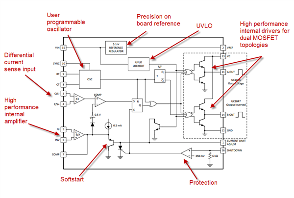
Take a look at what’s under the hood of one of these devices.

Figure 1: UC3846 Block Diagram

You have drivers, control and protection: all of the key must-have elements. Because you have access to the key comparator and amplifier inputs and outputs, you have a tremendous amount of freedom to make the device do precisely what you need it to do. Here are a few examples I can think of off the top of my head:

  • Summing the C/S inputs with the RT/CT ramp enables peak current-mode control with slope compensation.
  • Directly feeding the C/S inputs with a ramp achieves voltage-mode control. If you make this ramp proportional to the input, you have input voltage feed-forward on a cycle-by-cycle basis.
  • The internal operational amplifier has its input and outputs exposed for complete customization of the compensation.
  • You can use the external circuits for pull down or up on the COMP pin to shut down or introduce some flavor of nonlinear control.

While that doesn’t necessarily have the same level of flexibility found in digital control, it brings a boat-load of similar flexibility benefits that excite a geek like me.

What kind of uses do you have for general-purpose PWM controllers? What flexibility do you value most in these kinds of devices? I’d love to hear your thoughts on this subject in the comments section.

TI has a large selection of general-purpose PWM controllers to satisfy your every need, from the eight-pin UCC28083 to the automotive-qualified LM25037-Q1.

Additional resources

It’s hip to be square

$
0
0

All power stage designers like to see a perfect square waveform at the switch-node. Fast rising/falling edge reduces switching losses, and low overshoot and ringing minimizes voltage stresses on the power FETs.

Designed with TI’s latest GaN technology, the power stage’s switch-node waveform shown in Figure 1a, looks truly impressive, from 0V to 480V at a 120V/ns slew rate, with less than 50V overshoot. 

Figure 1:  TI’s 600V half bridge power stage - switching waveform (a); device package (b); picture of half bridge board (c).

GaN FETs have low terminal capacitance, and thus enable fast switching. When a GaN half bridge switches at high di/dt, however, the power-loop inductance introduces ringing/overshoot at the high-voltage bus and switch node. This limits how fast the GaN FETs can switch.

Traditional power packages often have high inductance from both leads and bond wires due to long leads and large package sizes. Overshoots as high as a few hundred volts have been observed with leaded packages. The key to reducing overshoot is to minimize the power-loop inductance.

To reduce lead inductance, TI offers its single channel GaN power stage products in surface-mount quad flat no-lead (QFN) packages. As shown in Figure 1b, TI designs the power loops and gate loops to have low inductance internal to the QFN. TI’s GaN half-bridge evaluation module (EVM), shown in Figure 1c places the high and low side devices and bus capacitors close together and returns the power loop at the board layer immediately underneath the devices. This minimizes the size of the power loop, thus keeping the loop inductance low.

TI’s advanced packaging and board design reduces the power-loop inductance to a few nano-Henries. This low-inductance design, integrated with an optimized driver, enables the LMG3410 to switch at slew rates >100V/ns with less than 10% overshoot. With the LMG3410, you can design power converters to switch fast for better efficiency, with low-voltage overshoots and reduced electromagnetic interference (EMI).

TI’s LMG3410 GaN power stage enables power-supply designers to develop higher-density and higher-efficiency power supplies. The device’s ability to reliably switch at high slew rates, combined with an integrated driver with over-current and over-temperature protections, simplifies your job of developing industry-leading power solutions.

Additional resources:

Selecting voltage detectors, supervisors, and reset ICs for system safety: part 2

$
0
0

In the first installment of this series, I defined voltage detectors and supervisors/reset ICs and explained different output types, along with some basic devices. As designs become more complex, more advanced devices may be required to successfully monitor a voltage. In this installment, I’ll highlight various features found in voltage detectors and supervisors/reset ICs to help designers select the right one.

Programmable output delay

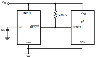
Voltage supervisors, unlike voltage detectors, usually have a programmable output delay using an external capacitor, making them extremely flexible. They are useful for the proper sequencing of multiple supplies, such as in field-programmable gate array (FPGA) applications or to prevent system glitches. When the supply voltage rises above the voltage threshold (plus the hysteresis, if applicable), this would normally trigger the device to “unflag” the reset signal and return the system from a reset condition. Since there is a delay created by the delay capacitor (CD), however, the voltage must remain above the voltage threshold plus hysteresis for the specified time delay before the reset signal unflags. This prevents the system from returning from a reset condition prematurely.

Programmable output delay is sometimes referred to as a programmable reset timeout period. A ceramic chip capacitor connected directly to the delay pin (sometimes named CD or SRT) is usually sufficient for a stable, well-defined output delay. The LM8365, shown in Figure 1, has a programmable output delay.

Figure 1: LM8365 typical application circuit with programmable output delay

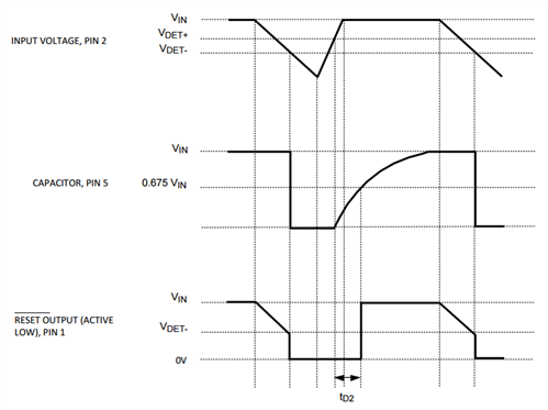
When the input voltage drops below the reset threshold, the reset pins drops low. When the input voltage rises above the threshold, there is a delay before the reset pin comes back up. By increasing the capacitor (CD), the delay increases. See the timing diagram for the LM8365 in Figure 2.

Figure 2: Timing diagram for the LM8365

Manual reset

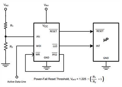
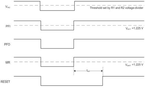
A manual reset input forces a reset when the manual reset (MR) pin is lower than the manual reset threshold (VMRT) for a specific duration, usually on the order of microseconds. The reset pin remains active as long as the MR pin is held low. The pin releases once the reset timeout period expires after MR rises above the VMRT. This feature is useful for microprocessor applications when the user needs to reset. It’s also useful in applications that need to reset when detecting a low voltage other than the main supply voltage. Manual reset gives you full control over the reset rather than having only a low supply-voltage trigger.

Power-fail input

Some voltage detectors and supervisors/reset ICs have an additional input for a power-fail warning to monitor a power supply other than the main supply. This additional input can be useful in systems that want to detect if the power is failing before it actually fails. The threshold can vary with different devices, but a typical threshold value is 1.225V from an internal reference. If the power-fail input (PFI) pin is lower than the power-fail voltage threshold (VPFT), the power-fail output (PFO) drops low.

Typically, the power-fail comparator, driven by a voltage divider connected to the main supply, signals a falling power supply. A voltage at PFI that drops below VPFT several milliseconds before the main supply voltage drops below the reset threshold provides advanced warning of a brownout. The PFI pin can also connect to the MR pin to force a low output signal for voltage detectors or a reset for supervisors/reset ICs.

Watchdog timer

Voltage detectors and supervisors/reset ICs with watchdog timers wait for signal activity on the watchdog input (WDI) pin. A reset triggers if the supervisor does not detect a signal within the watchdog window. You can program this window using an external capacitor, making the watchdog window more flexible.

A watchdog timer is usually for safety-critical applications or for processor monitoring that requires a reset if the microprocessor is not active for a certain duration. This feature prevents the system from continuing to run if the microprocessor is not functioning properly.

Low-line output

This early power-failure warning indicator goes low when the supply voltage drops to a value higher than the reset threshold. The indicator triggers about 2% above the reset threshold to indicate low power without causing a reset.

Figure 3 shows an example application circuit for the LM3710, while Figure 4 shows an example timing diagram with examples of the features I’ve reviewed so far.

Figure 3: LM3710 application circuit

In addition to the standard reset, the LM3710 has a manual reset, power-fail input, watchdog timer and low-line output, making it a very flexible device for many applications. The application circuit shown in Figure 3 above uses R1 and R2 as a voltage divider connected to VIN2 to set the power-fail reset threshold in order to monitor a second power supply. If the second power supply drops below the power-fail reset threshold, the PFI pin will be low, so the PFO pin will also drop low. Since this pin is connected to the MR pin, a reset will trigger.

A reset will also occur if no activity is detected within the watchdog window on the WDI pin. The WDI pin can connect to the microprocessor to detect if it is still operating correctly by having the microprocessor send an intermittent pulse. The low-line output (LLO) pin will drop low if the supply voltage at VCC drops to within about 2% of the reset voltage threshold. The LLO pin, for example, can connect to a microprocessor for detection. When the LLO pin goes active, a signal sent to the microprocessor can cause some other action to occur such as sending a signal to another device or a flashing LED or some other alert to the user.

 Figure 4: Example timing diagram for power-fail and manual resets of the LM3710

The timing diagram in Figure 4 shows an example of monitoring a second voltage input (VIN2). When the VIN2 connected to the PFI pin goes low, the PFO pin drops low, causing the MR pin to drop low, which then triggers a reset. There are many ways to use the power-fail and manual reset features, so it is up to you to decide what you need for your application.

After reading Part 1 and Part 2 of this blog series, you should be aware of the subtle difference between voltage detectors and voltage supervisors/reset ICs along with the various features that are available. There are countless applications that require detecting a supply voltage beyond a set voltage threshold and it is up to the designer to determine what happens next. When your battery is low, for example, do you want your system to flash a light or turn on a speaker or turn off some other device in your circuit? Do you want the user to be able to press a button to trigger this same condition or some other condition? Do you want to be able to monitor multiple voltages at different thresholds? When choosing a voltage detector or supervisor/reset IC, first determine what you are trying to do and what features you need then you can narrow down the devices by the specific specs, package, cost, etc. To see all of the voltage detectors and supervisors/reset ICs offered by Texas Instruments, see the voltage detector and supervisor/reset IC selection guide website.

USB PD 3.0 fast role swap switching considerations

$
0
0

The introduction of USB Type-C™ and USB Power Delivery (PD) will forever change the way we interact with our notebooks/tablets/smartphones and accessories  A single cable provides both power and data, without any pre-disposition toward which end or device is the host or client. Power can be sourced from both ends or devices and power roles can dynamically change as conditions warrant. With USB PD 2.0 devices hitting the market, we immediately witnessed several uses cases pushing the bounds of what we thought possible.

Figure 1 shows a common configuration of host, hub and peripheral. The intent is to charge the host via the hub while powering both a hard drive and maintaining a lossless image on a monitor. But what happens when you remove the charger plug?

Figure 1: USB PD Host Powered by USB PD Hub

Well it depends, and that is the issue at hand. In many systems, the power role swap was not quick enough; the data and video connection failed for a brief moment as the USB PD host became the power source. Other systems entered an alternate mode (such as TI’s quick swap) upon the establishment of the original power roles, ensuring that a stable voltage was available even if the charger was removed from the USB PD hub.

Figure 2: USB PD Hub Powered by USB PD Host

Although designers found a way to solve this problem using USB PD 2.0, it was clear that a common methodology was necessary to provide interoperability and consistency among devices.

The new USB PD 3.0 specification introduces a solution to provide a more consistent user experience across the USB Type-C and USB Power Delivery ecosystem. The original source must recognize that power has been removed and initiate a power role swap. The original sink must apply power to the original source much faster than allowed during a normal PD voltage change. These two components allow the original source to maintain power during a power loss condition.

Fast role swap initiates when the source pulls the CC line below 490mV for 60-120µs. Figure 3 shows the signaling components integrated into the TPS65983B. As you can see, a low-resistance pulldown is available on each CC line.  When the power has been removed, the TPS65983B internal controller will enable these pulldowns for the appropriate amount of time, signaling to consumers that a fast role swap is about to take place.

Figure 3: CC Fast Role Swap Signaling

After receipt of the fast role swap message, the host must act very quickly.  It has less than 150µs to assume the source role and provide up to 5V at 3A. Under normal conditions and assuming the typical 30mV/µs, the turn-on time for a 5V supply is approximately 158µs. In order to meet the new specification, a much quicker and dynamic solution is required. Fortunately, the TPS65983B integrates both the source and sink power paths. It has the ability to dynamically change the switching time of the internal power FETs to meet the new timing requirements and can dynamically reconfigure the current-limit setting to handle the increased in-rush current caused by the quick turn-on time. Figure 4 below shows the VBUS handoff from the old source to the new source to maintain a constant supply on VBUS.

Figure 4: VBUS During Fast Role Swap

USB Type-C and USB PD can now provide the necessary framework to enable to complete the user experience. The TPS65983 not only provides the required USB PD 3.0 signaling, but also includes the power FETs and power-path control to complete the implementation of fast role swap. Proprietary or discrete implementations will no longer be required. With the TPS65983B switching it quick has never been easier.


Additional resources:


Viewing all 437 articles
Browse latest View live


<script src="https://jsc.adskeeper.com/r/s/rssing.com.1596347.js" async> </script>