Quantcast
Channel: Power management
Viewing all 437 articles
Browse latest View live

Design a pre-tracking regulator, part 2: for a negative LDO

$
0
0

By Arief Hernadi and Frank De Stasi

The first installment of this two-part series demonstrated how to create a tracking pre-regulator for a positive output low-dropout regulator (LDO). In this installment, we’ll use a similar technique to create a tracking pre-regulator for a negative output LDO. This example will use the same LMR33630 evaluation module (EVM), but in the inverting buck-boost configuration in conjunction with the TPS7A3301 LDO.

One sample application for a negative LDO is to provide a negative voltage rail for an amplifier. Figure 1 shows a modification to the LMR33630 feedback network in order to create pre-tracking regulator for negative output LDO.

Figure 1: A negative-tracking pre-regulator with the LMR33630 and TPS7A3301

Modifying the TPS7A3301 EVM feedback resistor generates a -5-V output at the LDO; the LDO output voltage connects to the base of the 2N3904 N-channel P-channel N-channel (NPN) transistor. The LMR33630 internal reference voltage is 1 V with respect to the GND pin. Therefore, the voltage at the FB pin of the LMR33630 will be regulated at 1 V with respect to the GND pin of the device, which is now the negative output of the DC/DC converter.

As shown in Figure 1, the voltage across RFBB is also equal to 1 V. This in turn will create a reference current flowing in RFBB with a value of IFBB = 1 V/1 kΩ = 1 mA.

This IFBB reference current will then be mirrored by Q1/Q2-matched P-channel N-channel P-channel (PNP) transistors to generate the collector of Q3, which flows through resistor R1 (IC ≈ IE of Q3).

With IFBB ≈ IR1 ≈ 1 mA and approximating to 0.6 V, you can then calculate the expected output voltage of the DC/DC converter as:

In this case, the voltage output of the DC/DC converter stage will be approximately 2.1 V lower than the output voltage of the LDO.

As you can see from the calculation, it’s possible to approximate the voltage difference between the input and output of the LDO with Equation 1:

During design, you have to make sure that the DC/DC converter provides enough negative voltage to start up an LDO. Choosing a proper value for the R1 resistor can control this voltage.

In this example, the TPS7A3301 has a typical undervoltage lockout of -2 V. When the LDO is still off, and the input of the DC/DC converter is applied, the output of the LMR33630 will start going negative while the output of the LDO is still at 0 V.

The initial current that flows in the Q2 in Figure 1 is approximately 1 mA (1 V/1 kΩ). During initial startup and also illustrated in Figure 2, the VOUT DC/DC voltage is:

As you can see, you have to choose a proper value of resistor R1 to generate a sufficient voltage to start up the LDO that a user choose in their application.

Figure 2: Initial startup voltages off the LMR33630 and TPS7A3301

Figures 3 and 4 illustrate the startup and shutdown waveforms for the example negative-tracking pre-regulator circuit.

Figure 3: Startup waveform for a 12-V input at the DC/DC converter (CH1 = VIN, CH2 = VOUTLDO, CH3 = VOUTDCDC, CH4 = IOUTLDO)

Figure 4: Zoomed-in startup waveform for a 12-V input at the DC/DC converter (CH1 = VIN, CH2 = VOUTLDO, CH3 = VOUTDCDC, CH4 = IOUTLDO)

In Figures 3 and 4, the output of the DC/DC converter is 1.925 V lower than the LDO. There is a small discrepancy between the calculations and experimental value (1.925 V vs. 2.1 V); this is due to the matching current in the PNP pair. Having a co-packaged PNP improves this matching compared to a discrete type, but there will be a small discrepancy in the current between the pair. One way to improve the matching is to make a Wilson current mirror to generate the reference current, as described in Akshay Mehta’s blog post, “How to Create a Programmable Output Inverting Buck-Boost Regulator.”

Figures 5 through 8 are some scope captures on the shutdown performance of the circuit shown on Figure 2. Figure 9 shows the modified LMR33630EVM and TPS7A3301EVM PCB board in order to implement the tracking functionality.

Figure 5: Shutdown waveform for a 12-V input at the DC/DC converter (CH1 = VIN, CH2 = VOUTLDO, CH3 = VOUTDCDC, CH4 = IOUTLDO)


Figure 6: Zoomed-in shutdown waveform for a 12-V input at the DC/DC converter (CH1 = VIN, CH2 = VOUTLDO, CH3 = VOUTDCDC, CH4 = IOUTLDO)


Figure 7: Load-transient waveform at the output of the LDO with a 200-mA step load (CH1 = VIN, CH2 = VOUTLDO [AC-coupled], CH3 = VOUTDCDC [AC-coupled], CH4 = IOUTLDO)

Figure 8: Load-transient waveform at the output of the LDO with a 500-mA step load (CH1 = VIN, CH2 = VOUTLDO [AC-coupled], CH3 = VOUTDCDC [AC-coupled], CH4 = IOUTLDO)


Figure 9: Board picture for a negative-tracking pre-regulator

Together with a positive-tracking pre-regulator, you can see that both circuits can increase your system efficiency when you are designing something that requires an LDO as your point-of-load power supply.

When failure isn’t an option: power up your next satellite with integrated functionality and protection

$
0
0

Satellite building is hard.

Complex applications like communications, navigation and Earth observation demand insanely complex electrical and software engineering. With numerous sensors, field programmable gate arrays (FPGAs) and integrated circuits (ICs) drawing more power, designers must distribute components more widely to increase efficient power use and load balancing.

Each of these components also has different demands, with a single source often required to deliver power at multiple voltages and currents. A modern satellite might be home to thousands of points of load (PoL), yet a single charged particle impacting a sensitive PoL switch could cause catastrophic failure to millions of dollars’ worth of hard-to-replace equipment.

Thus, from a project’s inception, designers must build every component to exacting standards and integrate redundancies and safety features to prevent such failures, despite the crazy forces and vibration of launch and, once in space, a punishing environment characterized by radiation and temperature extremes.

With integration comes reduced complexity

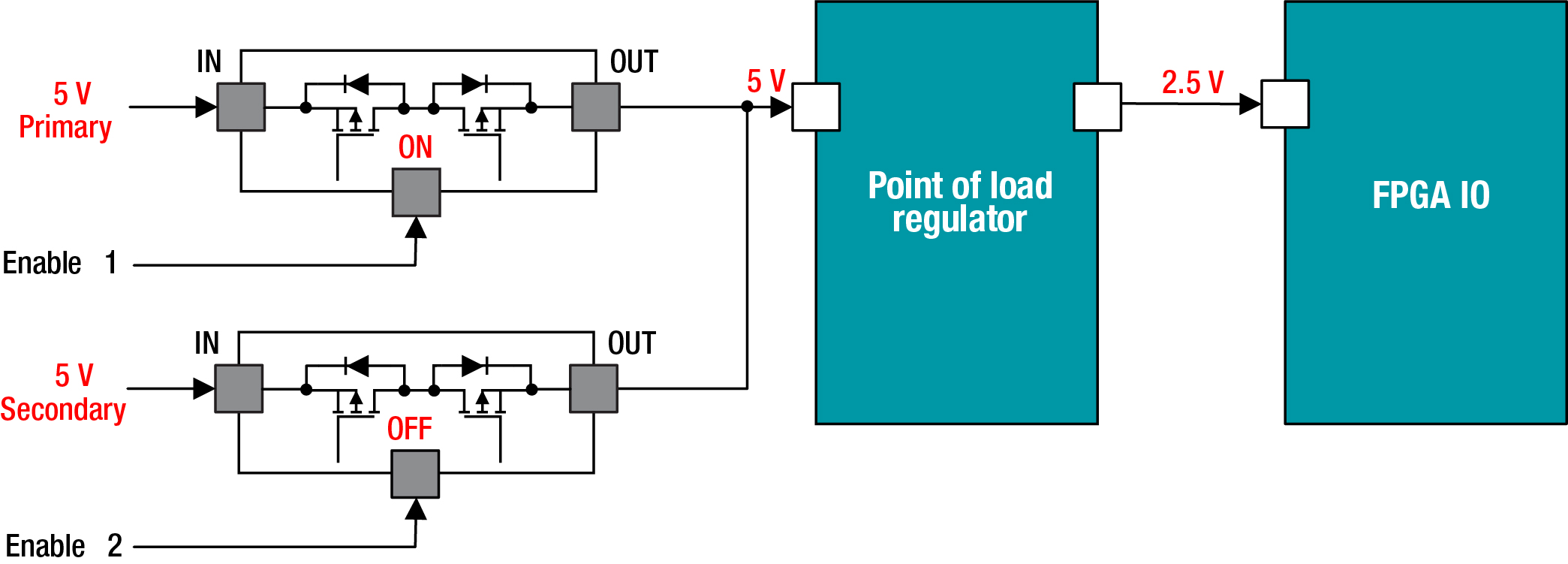
The TPS7H2201-SP space-grade integrated smart load switch is a first–to-market monolithic IC solution that delivers high power density, electronics protection and improved functionality. The device helps decrease board size and weight, reduces the risk of failure from using multiple parts and requires less work to achieve board power requirements. The switch doesn’t compromise safety for a smaller footprint; it increases and improves monitoring, power supply and load protection, and is able to provide redundancy simultaneously. Figure 1 shows a redundancy application using the TPS7H2201-SP.

Figure 1: Block diagram of a cold sparing application

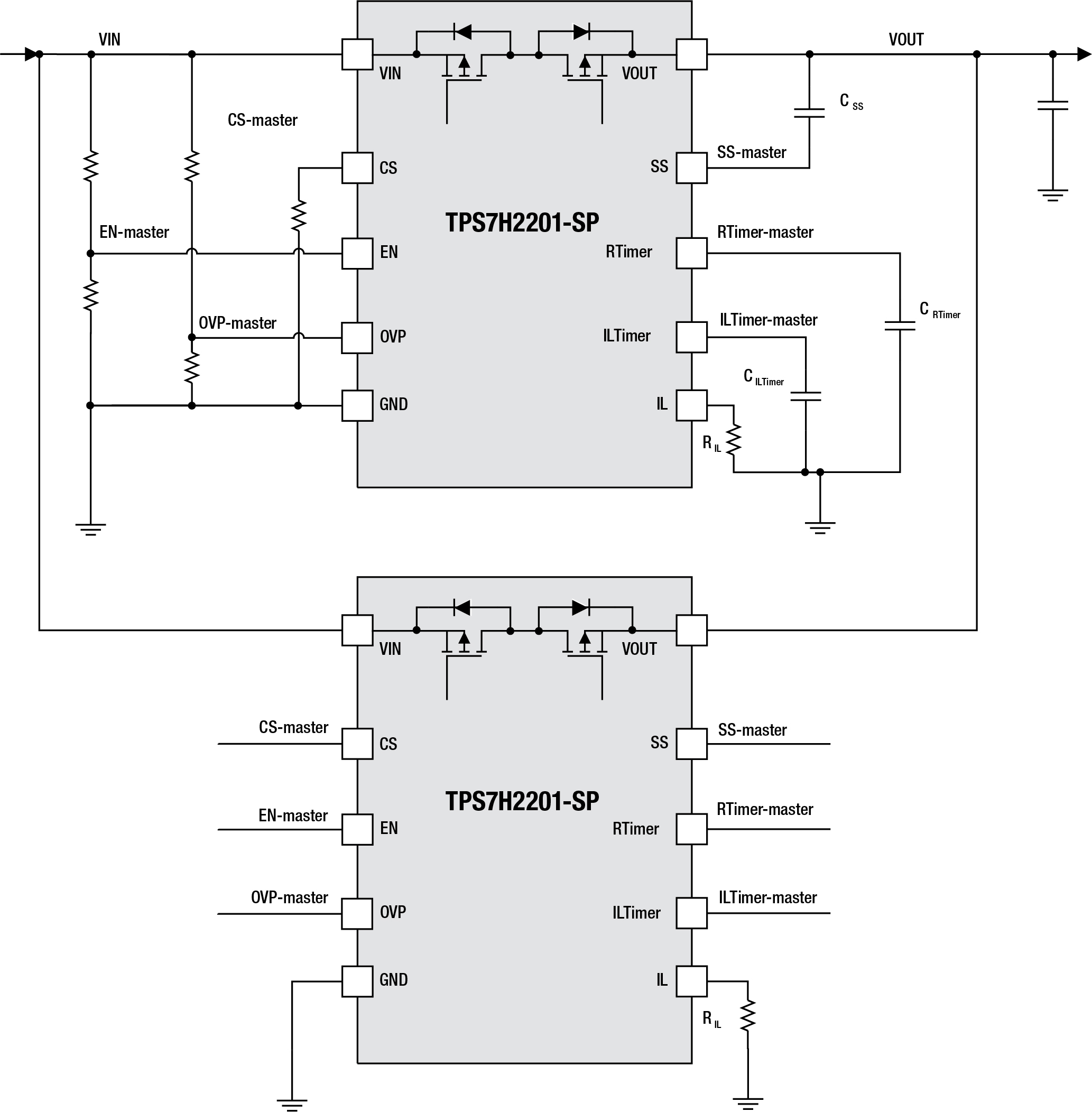
The device has an input voltage range from 1.5 V-7 V and supports a maximum continuous current of 6 A. You can connect multiple units in parallel to achieve higher currents as shown in Figure 2. Internal logic allows autonomous functionality, which eliminates the need for an external microcontroller.

Figure 2: Block diagram of a smart load switch used in parallel

The TPS7H2201-SP can shrink a board’s load-switch solution by 50% compared to previous discrete components. Integrating many pieces into one translates to weight reductions that can also decrease launch costs.

TI also upgraded the switch to provide advanced current protection – integrating reverse-current protection and overcurrent detection and protection – reducing reliance on past generations of electromechanical devices. Downstream devices get overcurrent, overvoltage and monitoring protection.

To endure the unique rigors of space, the TPS7H2201-SP can withstand total ionizing radiation doses of up to 100 kilorads, a level of protection that is more than enough to safely operate in geosynchronous orbit for at least 20 years. TI also tested the device to ensure that it would function through destructive single-event effects caused by cosmic-ray bombardment with heavy ions.

Conclusion

Our space-ready IC portfolio offers industry-leading specs in power density, size and efficiency. You can rest easy connecting the most sensitive imaging, communications, attitude and propulsion control payloads to a power rail managed by TI products.

The TPS7H2201-SP switch joins TI’s spaceflight-proven complete portfolio of radiation-hardened power-management components, which include the:

  • TPS50601A-SP single-output 6A space-grade DC/DC converter.
  • TPS50602-SP dual-output 6A, or single-output 12A space-grade DC/DC converter.
  • TPS7H1101A-SP 3A output radiation-hardened low-dropout regulator (LDO).
  • TPS7A4501-SP wide-input-voltage radiation-hardened LDO.

Fewer component requirements, technical documentation like radiation reports and reference designs, and a guaranteed continuity of supply all translate to shorter design cycles, greater confidence, and less weight and area needed for space applications, from communications and navigation satellites to science and earth observation platforms.

Additional resources

How to choose a DC/DC converter for a storage application

$
0
0

Driven by the global cloud computing development and continuing construction of data centers, shipments of global storage equipment are experiencing explosive growth. As the key part of the storage equipment, the demands for DC/DC converters that power the storage equipment (solid-state drive [SSD] and memory) also show a relatively rapid growth trend.

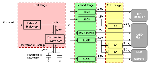
Figure 1 shows a simplified power architecture for an enterprise solid-state drive (SSD). The first stage is the protection and backup circuit; the input voltage of this application is normally 12 V. The second stage requires DC/DC converters for higher current (>6 A). In the third stage, low-dropout regulators are added in the rails, which are very sensitive to voltage fluctuations.

Figure 1: A simplified power architecture of an enterprise SSD

In this SSD, the DC/DC converters need to fulfill several requirements: small output voltage fluctuation, high efficiency and small solution size.

Except for those very sensitive rails, the rest of the power rails supplied by buck converters also need less voltage output fluctuation To not only support the low output voltage ripple in constant load (less than 1% * VOUT even at full load), but also provide a small overshoot/undershoot in load transient. This is because large voltage fluctuations will have a risk of NAND deterioration and controller instability, which will shorten system lifetimes or even cause damage.

There is no exception that efficiency is an important indicator for DC/DC converters in most applications. High efficiency can prevent power loss and improve thermal performance. High efficiency is also very critical for SSDs because excessive temperatures will slow down input/output per second and could damage the SSD.

With the explosive growth of data, engineers want to put more and more storage units in one data center. This also challenges the solution size of DC/DC converters. Not only does it require a smaller size to provide higher power density, but it also has more demanding requirements for height.

Given these demanding requirements – especially the output ripple – engineers will add more and more capacitors (200 -~500 µF in 8 A) in the output to keep the ripple at a small voltage. But adding more capacitors will not only attenuate the performance of the load transient, it will expand the solution size and increase the bill-of-materials cost. So there has to be a trade-off between the output stability and solution size, even though a larger solution size can help thermal dissipation.

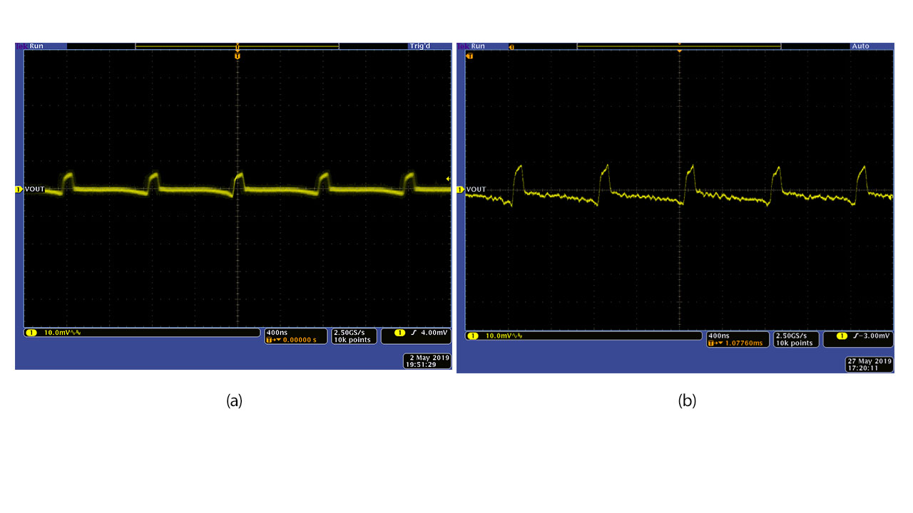
Figure 2 is a schematic of TI’s newly released TPS568230. It is an 18-VIN, 8-A buck converter with D-CAP3™ control mode that provides a fast transient response with no external compensation components and an accurate output voltage. It can achieve an output ripple that is less than 10 mV at full load and also a faster load transient response with only four pieces of 22 µF *4pcs at a 600-kHz switching frequency, as shown in Figure 3. The load step is from 2 A to 6 A with a 2.5 A/µS slew rate. The peak-to-peak output voltage ripple is only 55 mV, which can effectively avoid the NAND deterioration and associated damage risks.

Figure 2: TPS568230 step-down converter schematic


Figure 3: Output ripple with full load (a); load transient performance (b) (VIN = 12 V, VOUT = 1.05 V, FSW = 600 kHz)

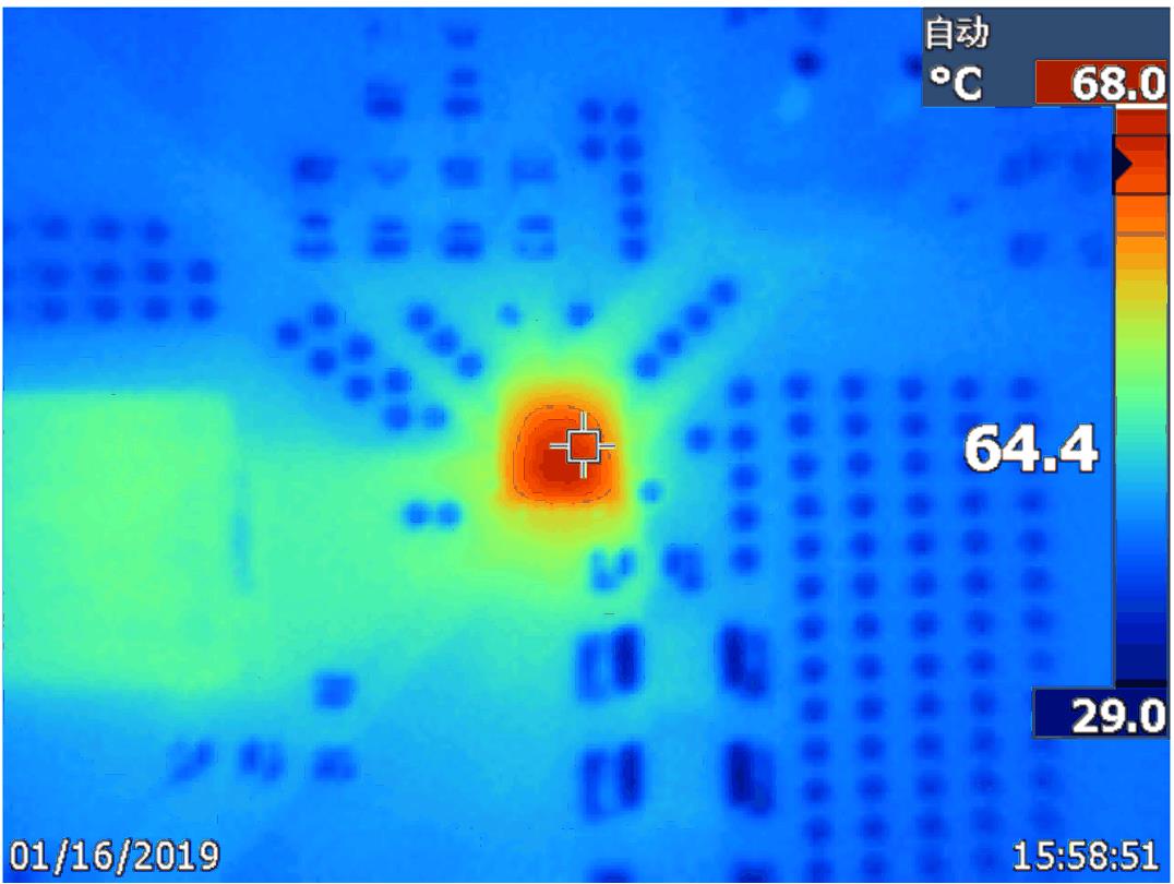
With low RDS(on) (19.5 mΩ high side, 9.5 mΩ low side), the TPS568230 offers good efficiency. Figure 4 shows the thermal performance.

Figure 4: TPS568230 thermal performance (VIN = 12 V, VOUT = 1.05 V, IOUT = 8 A, FSW = 600 kHz, 10 minutes)

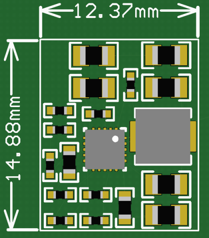
The package size of the TPS568230 is only 3 mm by 3 mm2 and the highest 1-MHz switching frequencies can also help adapt to high power-density applications. Particularly worth mentioning is that at a 1.05-V output voltage and 1-MHz switching frequency, the value of the inductor is only 0.33 µH (Würth: 744373240033, 4.45 mm by 4.06 mm by 1.8 mm), which can save both power solution size and height. Figure 5 is a model of the printed circuit board. The total solution size is less than 185 mm2 and the height is less than 2 mm.

Figure 5: Solution size with 1-MHz switching frequency

The TPS568230 satisfies fast load transient and high power-density requirements, as well as decreasing bill-of-materials cost. It’s a good fit for storage applications as well as routers, switches and servers that have similar power rail requirements.

Additional Resources:

Hit the brakes on discrete LED circuit designs

$
0
0

In automotive lighting such as turn lights, brake lights and tail lights, LED circuit designs typically implement discrete components like bipolar junction transistors (BJTs). Discrete components are prominent for a few common reasons: they’re simple, reliable and cheap. Yet as the number of LEDs and project requirements grows, it may be worth reconsidering designing discretely. Let’s explore some common misconceptions.

Discrete designs are simple

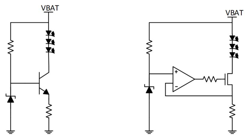
LEDs are current-driven devices. Using a transistor is the simplest way to switch on an LED with a regulated supply of current. These transistor-based circuits serve as fundamental building blocks that can be replicated to drive any number of LED strings across projects, as shown in Figure 1.

Figure 1: Constant-current discrete LED circuits

In projects that have a high LED count or challenging requirements, the circuit design not only looks crowded but also requires complex analysis. Crowded with BJTs to drive multiple LEDs, a rear combination light (RCL) module may include the specifications listed in Table 1.


Specification

Consideration

Implementation

Function

Same set of LEDs for tail lights and stoplights

Adjust brightness levels to indicate mode

Analog current or pulse-width modulation (PWM) dimming

Battery supply

Nominal: 9 V to 16 V

Range: 6 V to 40 V

Stable output current while withstanding voltage transients from start/stop, load dump, etc.

Constant current output circuit (see Figure 1)

Diagnostics

Open circuit

Detect fault and implement fault response

One-fail-all-fail (OFAF) circuitry

Table 1: Example RCL specifications

Using a high count of components like the RCL example in Figure 2 increases design and manufacturing risk, and you must carefully analyze the circuit.

Figure 2: Example discrete tail-light and stoplight circuit

Discrete designs are reliable

A robust LED circuit design must account for fluctuations in voltage, current and temperature. Once an LED’s forward voltage is reached, current flows; changes in current proportionally change the brightness. However, a small change beyond the forward voltage results in an exponential increase in LED current; too much forward current damages the LED.

You must also analyze power and thermal dissipation. Factors contributing to temperature increases include poor power efficiency from the circuit, duration of the LED’s on time, and/or a warm environment. Poor thermals cause LEDs to consume too much current and thus degrade.

Feedback circuitry to diagnose LED open-circuit or short-circuit failures improves system reliability. While such circuitry adds more components, there are advantages. For example, if an LED breaks within a RCL, then the module’s brightness is no longer compliant with market regulations. The body control module (BCM) may have difficulty distinguishing between a valid LED load and a single open load from a lighting module, as shown in Figure 3. In the event of a broken LED, implementing OFAF circuitry will turn off all LEDs and make it easier to detect an open load. OFAF also prevents further LED degradation.

Figure 3: A BCM diagnoses faults from the LED driving module

The LED circuit must meet emission and bulk current injection (BCI) immunity standards for electromagnetic compatibility (EMC). If you disregard EMC, the LED driving module could interfere with or be affected by other applications, creating a poor experience for drivers.

Discrete designs are cheap

BJTs are cheap commodity devices. However, when designing with dozens or even hundreds in a LED system, component count and system costs add up. Considering resources spent designing, debugging and assembling, it is possible to save time and money by using an integrated LED driver solution.

Linear LED driver integrated circuits (ICs) range from single channel for general use to multichannel devices for specific functions. As shown in Figure 4, an integrated solution like the TPS92611-Q1 can replace the multiple BJTs and other discrete components from Figure 2’s RCL circuit.

Figure 4: The TPS92611-Q1 with a fault bus connected for OFAF

In addition to lowering component count and system costs, linear LED drivers deliver a constant-current output with a low dropout voltage, and adjustable brightness via analog current or PWM dimming. Thermal protection and short- and open-circuit diagnostics provide solid performance, and an OFAF fault bus can be connected across devices to ensure system reliability. The TPS92611-Q1 and other linear LED drivers also offer strong EMC performance compared to discrete solutions.

A LED driver IC solution is a cost-effective alternative to discrete circuits, especially in applications with high LED count or complex requirements. With simple designs, reliable performance and cost competiveness, put the brakes on discrete circuits and switch to an integrated linear LED driver today.

Additional resources

Current sensing in battery management systems

$
0
0

While driving through cities across the world, it’s impossible not to notice the emerging presence of hybrid electric vehicles (HEVs) and electric vehicles (EVs). With the rapid growth of HEVs and EVs in the automotive market, systems such as battery management become significant.

Take, for instance, your cellphone’s battery. You’re constantly checking its status to ensure that you can use your phone throughout the day. Now translating this to a car, imagine how crucial such information becomes.

There are a variety of current sensing technologies that can monitor the status of an HEV or EV battery. The solution varies with the voltage and capacity of the battery. As shown in Figure 1, there are two main locations where you can measure current: top of stack (high-side sensing) and bottom of stack (low-side sensing).

Figure 1: Top of stack vs. bottom of stack in a battery management system

Typically, the batteries in electric vehicles are 400 V-800 V. In such a system, isolated current sensing solutions are preferable when performing top-of-stack current measurement.

TI offers multiple options for isolated current sensing. The DRV425 is an integrated magnetic fluxgate sensor integrated circuit that when implemented as a pair can be used for high-precision bus-bar measurement. TI also offers a family of isolated current sense amplifiers that can monitor shunts at the top of high-voltage battery stacks.

Bottom-of-stack current sensing in EV systems and both high- and low-side current sensing in 48-V/12-V HEV systems typically do not require isolated current sensing. 

For many years, current sense amplifiers have been implemented in applications used for current and power measurement. These simple and affordable solutions enable designers to achieve real-time overcurrent protection, system optimization and current measurement for closed-loop circuits with excellent linearity and accuracy. 

Depending on system requirements and designer preferences, the type of current sense amplifier required will vary. TI offers wide portfolios of current sense amplifiers with common-mode range, offset voltage, gain error and drift options. For HEV/EV battery management systems, the decision between current sense amplifiers with an analog or digital output may be important.


Learn more about how to implement current sense amplifiers in battery management systems


Watch the video series

As shown on the left side of Figure 2, current sense amplifiers with an analog output integrate gain-setting resistors and send an amplified signal to the single-ended analog-to-digital converter (ADC) based on the differential voltage measured across the shunt resistor. For analog output current sense amplifiers, the value of the shunt resistor depends on the full-scale output, maximum input current and gain. The minimum current is limited to the value of the shunt and the offset voltage of the device. The ADC reference will be an additional error source that requires evaluation in the signal path. While current sense amplifiers with analog outputs are still highly accurate and extensively used in battery management systems, current sense amplifiers with a digital output may offer additional value.

TI’s digital output current sense amplifiers (shown on the right in Figure 2) integrate a specialized delta-sigma ADC that eliminates the need to amplify the input signal to maximize the ADC’s full-scale input range across the shunt resistor. Due to the delta-sigma architecture, digital output devices have lower input offset voltages, which enable higher precision measurements at low currents. Thus, you can use a smaller-value shunt resistor for improved system efficiency.

Figure 2: Analog vs. digital output current sense amplifiers

Current measurement applications such as battery management systems require the robust performance offered by current sense amplifiers. TI’s portfolio of current sense amplifiers encompasses many needs, from wide common mode range, low offset voltage and small gain error.

Additional resources

Choosing the right SOA for your design: discrete FETs vs. power blocks

$
0
0

In power semiconductors, design engineers use the safe operating area (SOA) to determine whether it’s possible to safely operate a device such as a power metal-oxide semiconductor field-effect transistor (MOSFET), a diode or an insulated-gate bipolar transistor (IGBT) at current and voltage conditions in their application without causing damage to itself or nearby devices.

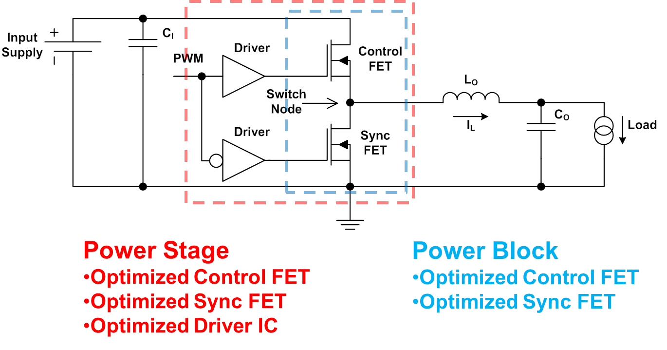
New integrated devices such as power blocks and power stages require a different way to specify SOA. As shown in Figure 1, a power block integrates control and synchronous FETs in a half-bridge configuration. A power stage adds a driver integrated circuit to the power block.

 TI’s definition of power blocks and power stages

Figure 1: TI’s definition of power blocks and power stages

A new approach to an old problem

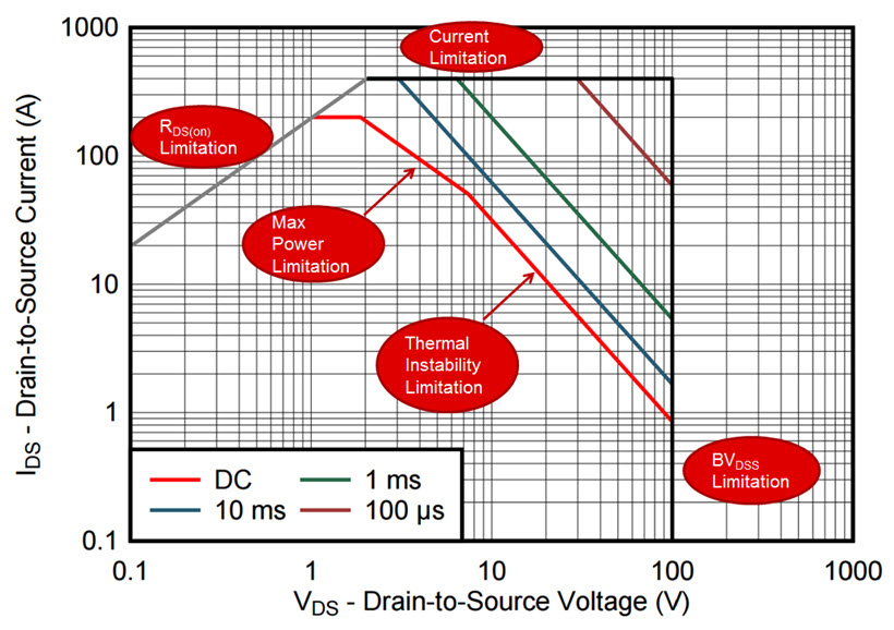
The purpose of this technical article is to illustrate the differences in how TI specifies SOA for single, discrete FETs vs. integrated power blocks. As explained in an earlier technical article, the SOA curves provided in TI’s discrete power MOSFET datasheets are for linear mode operation where drain-source voltage and current are present in the FET simultaneously. Under these conditions, the FET is dissipating high power, which can lead to catastrophic failure if the SOA curve is violated. Figure 2 shows the datasheet SOA curve for the CSD19536KTT power MOSFET.

 Datasheet SOA of the CSD19536KTT power MOSFET

Figure 2: Datasheet SOA of the CSD19536KTT power MOSFET

Unlike discrete MOSFETs, which fit into a multitude of applications, power blocks are optimized for use in switch-mode applications such as power supplies and motor drives. As such, discrete FET SOA curves don’t work for power blocks. To help designers, TI provides SOA information for power blocks in a way that correlates with the intended application.

SOA curves in TI power block datasheets are derived from power loss and thermal data collected with the device operating in an application circuit, such as a synchronous buck converter. Power blocks optimized for motor-drive applications are tested in a half-bridge configuration at a 50% duty cycle with a fixed output inductor. The SOA curves plot output current vs. temperature (printed circuit board [PCB] or ambient) and provide guidance on the temperature boundaries within an operating system by incorporating both thermal resistance of the package and system power loss.

Power-supply manufacturers provide similar SOA and thermal derating curves for their products. TI is leveraging this approach because power blocks are normally used in switch-mode power supply and motor drive applications.

Understanding power block SOA

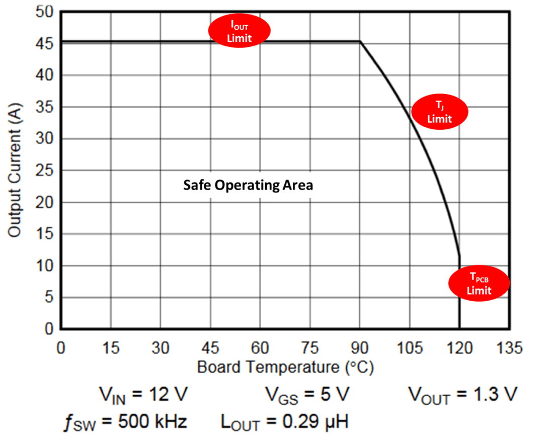
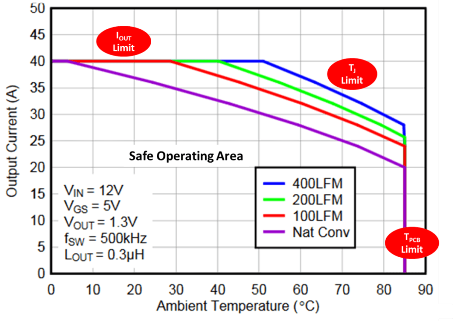
Figure 3 shows a typical datasheet SOA for the CSD87353Q5D power block in a synchronous buck converter, with the operating conditions provided below the figure.

 Typical datasheet SOA for the CSD87353Q5D power block

Figure 3: Typical datasheet SOA for the CSD87353Q5D power block

The region below the curve is the SOA for the power block and is defined by three distinct boundaries:

  • The horizontal line at the top of the graph is the maximum recommended output current for the application: 40 A.
  • The curved boundary to the right is the maximum junction temperature limit.
  • The vertical line on the lower right is the maximum PCB temperature limit – 120°C for most applications. This temperature may vary depending on the PCB material and your design specifications.

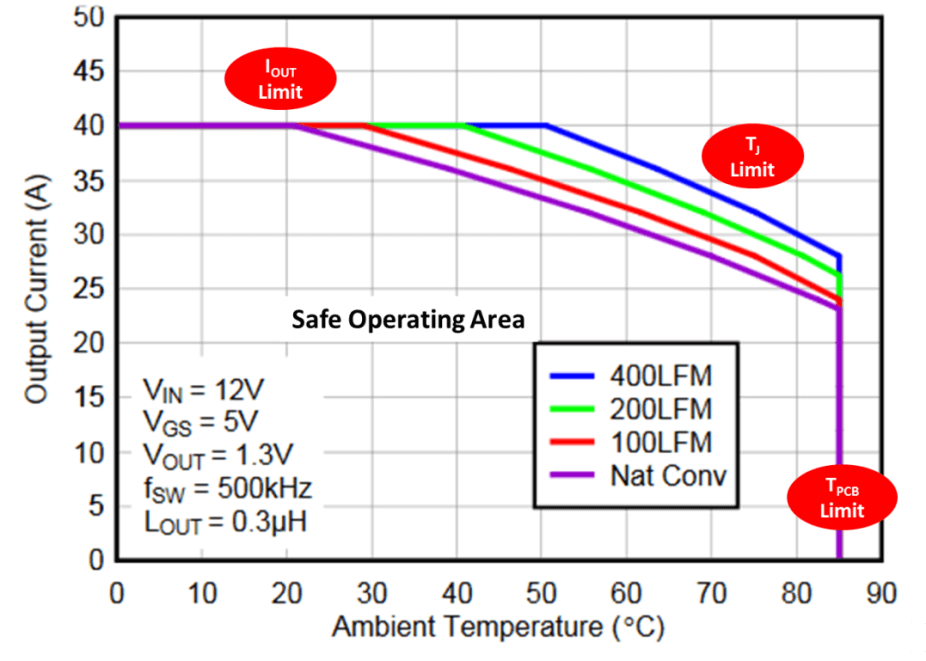
Figures 4 and 5 show datasheet SOA curves for the CSD87353Q5D and display the power block output current vs. ambient temperature in vertical and horizontal board orientations, respectively, with varying airflow conditions.

 CSD87353Q5D safe SOA – PCB vertical mount

Figure 4: CSD87353Q5D safe SOA – PCB vertical mount

 CSD87353Q5D SOA – PCB horizontal mount

Figure 5: CSD87353Q5D SOA – PCB horizontal mount

These SOA plots are based on measurements made on a 4-by-3.5-by-0.062-inch PCB design and six copper layers with a 1-ounce copper thickness each. As shown in Figure 3, the region below the curves is the SOA, with boundaries defined by the recommended maximum output current, maximum junction temperature and maximum ambient temperature in the application. In this case, TI chose 85°C as the maximum ambient temperature, as most power block applications fall within this limit. Again, this temperature can vary based on your application and requirements.

In addition to the SOA curves, the power block datasheet includes plots of measured power loss and normalized graphs that allow you to calculate adjustments to the SOA for your specific design and operating conditions. Detailed instructions and design examples are included in the Application and Implementation section of the power block data sheet.

The SOA is critical when determining whether a power device can operate in your application without damaging itself or devices around it. TI provides SOA data for integrated power blocks based on power loss and thermal data tested in an application circuit, an approach that correlates with how the device is used in your design. TI leverages the industry-standard SOA and thermal derating approach used for many years by power-supply manufacturers allowing you to confidently design the power block into your application.

Additional resources

Protector, monitor or gauge – selecting the correct battery electronics for your Li-ion-powered system

$
0
0

Lithium-ion batteries have high energy density and a long cycle life; they also lack the memory effect of other technologies. Such characteristics make them attractive for portable electronic systems. But lithium-ion batteries also need to operate within specified limits to be used safely, so batteries require electronics designed to respond or provide a signal to the system if the limits are exceeded.

Battery electronics monitor multiple conditions such as voltage, current and temperature and how they change over time. They need to sense the required combination of these parameters in order to respond, whether that’s sending a signal to the system, activating a switch to prevent charge or discharge, or opening a fuse. Figure 1 below shows an example of how the battery electronics might be configured in a typical battery pack.


Figure 1: Battery electronics within a battery pack

The type of battery electronics varies depending on the type of battery pack. Simple packs may need only a simple protector, ranging from a basic overvoltage protector to a more advanced protector that responds to under-voltage, temperature faults or current faults. Protectors can also operate as a secondary device along with a monitor or battery gauge.

Many advanced battery packs used in higher-cell-count batteries require a battery monitor. A battery monitor measures individual cell voltages, battery current and temperature, and reports these values to a gauge or microcontroller. The system uses this information to adjust performance accordingly; for example, by reducing the operating current if the temperature is too high. Battery monitors may provide a cell-balancing feature to extend battery run times as well as battery lifetimes. Monitors can also include protections available in integrated circuits (ICs), but with much higher configurability.

A gauge IC integrates the features of a battery monitor with a controller to provide advanced gauging algorithms. Gauge ICs report the remaining battery capacity, run time and state of charge. Software-based algorithms can enhance protections even further. Gauges often include other useful features such as a black-box function that helps diagnose battery packs that failed in the field, lifetime data logging of minimum and maximum parameter conditions, dynamic charger control, or authentication for secure batteries.

Figure 2 below outlines some of the key feature differences between the different types of battery electronics.

Figure 2: Feature differences between protectors, monitors and gauges

What features are most critical in choosing the optimal battery electronics for your system?

When evaluating the pros and cons of each battery electronics option, it’s important to consider the following characteristics of each:

  • Protectors offer the lowest complexity for simple pack designs.
  • Monitors offer the highest flexibility. You can write code specific to your system needs, which is often important when those needs are unique.
  • Gauge ICs offer the highest level of integration. They offer high-accuracy state-of-charge information and faster development time – since firmware is included – but might limit flexibility.

Figure 3 shows an example solution using the BQ769x0 battery monitor. The family includes devices for five- (BQ76920), 10- (BQ76930) and 15-cell (BQ76940) batteries. You can use the same controller software for any of the devices in the family, enabling flexibility for systems to go from three to 15 cells in series. The monitor continuously measures cell voltages, temperature and current through the sense resistor and reports this information to the microcontroller. It provides multiple configurable hardware protections and will open charge and discharge field-effect transistors (FETs) as needed to respond to fault conditions. The microcontroller can make decisions based on the information provided by the monitor – it can also enable/disable the FETs; control the cell-balancing feature; and even perform some basic gas gauging based on voltage, current and temperature information.


Figure 3: Example battery monitor solution featuring the BQ769x0 with a microcontroller

Figure 4 is an example of a slightly more advanced battery pack. Here, you see the same monitor family working with the BQ78350-R1 companion controller. The BQ78350-R1 comes equipped with firmware designed to work directly with the BQ7620, the BQ76930 or the BQ76940 digital monitor, helping accelerate product development. The BQ78350-R1 also performs fuel gauging and state-of-health reporting and includes many other features commonly included in TI fuel gauges, such as lifetime data logging and black-box recording.

Figure 4: Advanced battery pack featuring the BQ769x0, BQ78350-R1 controller with fuel gauge, BQ76200 high-side FET driver and BQ7718 secondary protector

Many systems require the redundancy of a secondary protector for overvoltage. This example features the BQ7718 stackable overvoltage protector, which can directly open a fuse if the primary protector fails.

Some systems may require the use of high-side FETs. High-side FETs enable continuous communication to the pack regardless of whether they are on or off. This means that the system can read critical pack parameters despite safety faults, and access pack conditions before allowing operations to resume. The BQ76200 high-side N-channel FET driver works well with the BQ76920, BQ76930 and BQ76940 monitors in systems needing high-side FETs.

There are many things to consider when designing systems with Lithium Ion batteries for safety and battery performance. Depending on the system needs, the appropriate protector, battery monitor or gauge can be selected.

Additional resources

Minimizing input power protection for smart speakers and smart displays

$
0
0

Smart speakers continue to enhance our homes with cutting-edge voice-recognition artificial intelligence and premium sound quality. When paired with other home automation devices – such as video doorbells, lighting systems, thermostats and security systems – smart speakers and smart displays are fast becoming the control hub for a smart home network.

To keep up with the growing market and stay ahead of the curve, designers are looking to reduce the size and heat dissipation of smart speakers while adding functionality and improving performance. Semiconductor devices that efficiently deliver higher performance in smaller packages become crucial to minimizing board space in space-constrained applications.

The majority of a circuit board comprises key components that directly influence the user experience, such as the audio system on chip, human interface controller for capacitive touch with haptic feedback, and LED driver engines and Class-D audio amplifiers. Other components in a smart speaker system such as power management perform essential tasks that do not directly impact the user experience, but do impact size and cost. It is possible to minimize these components for size while still maximizing performance.

One specific component is the input power-supply protection circuit, shown in Figure 1. Input protection, though sometimes taken for granted in many devices, is a critical circuit in the smart speaker to prevent damage to the entire system during power up or when connected to unreliable power supplies. Smart speakers are powered from either an external AC/DC wall adapter or an internal switched-mode power supply. This circuitry protects any downstream devices from being damaged in the event of a fault condition.
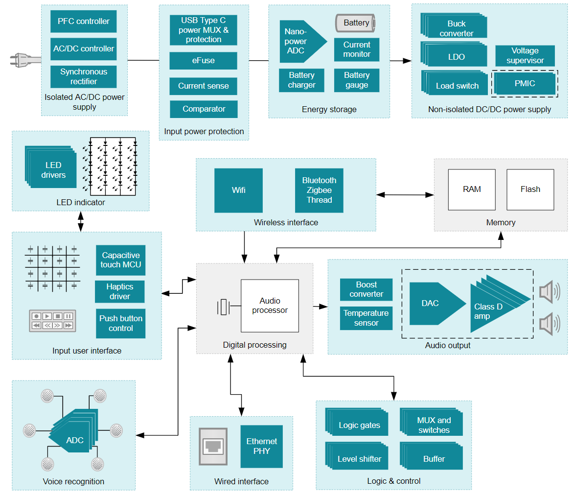
Figure 1: A reference block diagram showcasing the typical functions that make up a smart speaker

The primary concern on the input supply is an unnaturally high voltage or current event. TI has both integrated and discrete solutions to handle overcurrent protection (OCP) and overvoltage protection (OVP).

eFuse devices often handle OCP and OVP, integrating a power metal-oxide semiconductor field-effect transistor to disconnect all downstream circuitry under these fault events. eFuse devices also manage inrush current during startup, ensuring that system voltage increases in a controlled manner. Devices such as the TI TPS2595 offer this protection up to 18 V/4 A in a 2-mm-by-2-mm package.

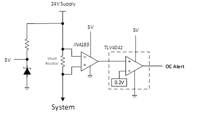
For OCP, a common discrete implementation involves a current-sense amplifier such as the INA185 to measure the current across a shunt resistor. The output of the INA185 either feeds into an analog-to-digital converter (ADC) to digitize the value for a measurement, or into a comparator to provide an instant alert to the microcontroller. The ADC path offers a precise measurement of the current flowing in the system, but adds delay in reading the measurement due to the sampling frequency of the ADC. The comparator path is about 1,000 times faster (while consuming less power) but only provides a digital output signaling overcurrent, not the actual value of the current.

The ADC method works for systems that need to precisely measure current in a system and have the flexibility to change limits dynamically. The INA185 offers better than ±0.2% full-scale accuracy and is the industry’s smallest current-sense amplifier in a leaded package. Measuring only 1.6 mm by 1.6 mm, the device is a great fit for space-constrained systems that require an optimized board layout.


Enhance the design of your smart speakers and docking stations


Learn more in our circuit about fast-response overcurrent event detection in smart speakers and docking stations.

In smart displays, however, the system voltages are above 18 V, and thus need a faster OCP alert. An integrated eFuse device may not be able to operate in such a system, but the combination of a current-sense amplifier and a comparator can offer the same functionality with increased flexibility while taking up minimal board space. Nanosecond-delay comparators like TI’s TLV4041 consume only 2 µA of supply current and can be powered off a simple Zener diode. When paired, the combined solution of the INA185 and TLV4041 measures 5 mm2 and delivers response times up to 50 times faster than competitive devices.

Using an amplifier like the INA185 with a fast comparator provides a quick and precise OCP alert when the system current exceeds a custom-set threshold. Depending on the system, this limit can be set anywhere from milliamps up to a few amps. The TLV4041 also has a precision (1% over temperature) integrated reference to provide an accurate alert regardless of the current level, all in a 0.73-mm-by-0.73-mm footprint.

The discrete solution shown in Figure 3 saves board space by eliminating the need for an additional on-board regulator, and also works in both low- and high-voltage smart speaker systems. The same circuit works across different speaker models of varying supply voltage levels to further simplify your input power protection designs.

Figure 3: Functional circuit showing how to set up the INA185 and TLV4041 to generate an OCP alert signal for high-voltage systems

The combined solution of INA185 (2.56mm2) and TLV4041 (0.533mm^2) take up approximately 5mm^2 of board space after including the necessary passive components. This total solution size is 15% smaller than comparable integrated devices that offer current sensing functionality. Moreover, TLV4041 has a delay of just 450ns, which makes TI’s combined solution considerably faster than those that integrate a general purpose comparator alongside a current sense amplifier.

The combined solution of INA185 (2.56mm2) and TLV4041 (0.533mm2) take up approximately 5mm2 of board space after including the necessary passive components. This total solution size is 15% smaller than comparable integrated devices that offer current sensing functionality. Moreover, TLV4041 has a delay of just 450ns, which makes TI’s combined solution considerably faster than those that integrate a general purpose comparator alongside a current sense amplifier.

TI’s broad portfolio covers multiple solutions to minimize input power protection in smart speakers. Whether it is low-voltage speakers requiring an integrated device or high-voltage speakers that could use a discrete implementation, TI provides small-size solutions without compromising performance.

Additional resources

  • This Application Brief discusses the trade-offs of using an amplifier and comparator for power-supply protection in further detail.


How to reduce the size of your 13-W PoE PD solution

$
0
0

You just got a big product out the door and are enjoying some well-deserved downtime when your product manager decides to swing by. Surprise, surprise: he wants the next-generation product to have more features and a smaller form factor. Luckily, you may be able to squeeze out some area from your Power over Ethernet (PoE) powered device (PD) solution.

If you’re after power density, consider the following when choosing a new PoE PD controller:

  • Does it integrate a PoE PD front end and a DC/DC controller? Does it have an integrated PD field-effect transistor (FET) and an integrated switching FET? Higher integration will usually save board space and streamline the supply chain, since fewer components need to be purchased and planned for.  For a robust solution consider a 100-V PD FET and a 150-V switching FET.  This will provide margin against variation of the clamping voltage of the input TVS and the ringing of the switching node in the Flyback.  
  • Does the PoE PD controller offer primary side regulation (PSR)? PSR is a crucial feature that will enable you to remove the optocoupler and shunt reference, along with the diodes and resistor capacitors used for soft start.
  • Does it offer spread-spectrum frequency dithering (SSFD)? This feature reduces electromagnetic interference (EMI) by spreading the noise in a broader frequency band.  SSFD typically results in a reduction of 4-6 dB at the fundamental switching frequency and 10-20 dB for higher-frequency harmonics, enabling a ~2x reduction in the high-voltage common-mode capacitors, which are usually big and expensive.
  • Does the PoE PD controller operate in continuous conduction mode (CCM) or discontinuous conduction mode? CCM has lower peak currents, which enables you to use lower input and output capacitors and injects less noise, thus requiring smaller filtering components.
  • Does it feature advanced startup? This feature provides full current to the DC/DC controller during the soft-start phase before the auxiliary winding is fully up. Advanced startup allows you to reduce the VCC capacitor from ~22 µF to 1 µF, enabling the use of a ceramic capacitor, which is smaller and more reliable.

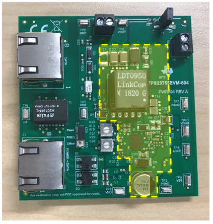
TI’s newly released TPS23755 is a Type 1 (limited to 13W of input power) PoE PD device that checks all of the above boxes.

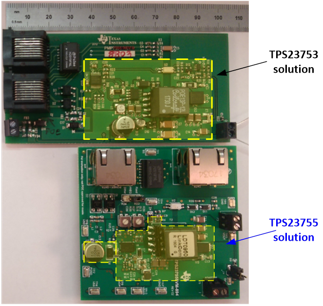
Figure 1 shows a visual comparison between a 12-V, 1-A solution for the TPS23753A vs. the new TPS23755 solution. Note that the figure does not include the EMI filter. The TPS23753A operates in CCM mode and integrates the PoE PD (integrated FET) with a DC/DC controller. The TPS23755 adds the integrated switching FET, PSR, advanced startup and SSFD.

Figure 1: Board Space comparison for TPS23755 vs. TPS23753

To appease your product manager and squeeze out some area from your PoE PD solution, consider evaluating TI’s TPS23755 evaluation module for IEEE 802.3at Type 1 PoE PD applications and “IEEE 802.3at Type-1 PoE and 12-V adapter input to point of load reference design for IP network camera” to get started with your Type 1 PoE design. For applications requiring 5V output consider evaluating TI’s TPS23758 evaluation module for IEEE 802.3at Type 1 PoE PD applications.

Additional resources

Changes to Power House

$
0
0

Thank you for following our company’s Power House blog. This week, we are refreshing the look and structure of the technical blogs on the TI E2E site to simplify how to find and select the relevant content for your interests.

Moving forward, you will find the content under the category of “technical articles” rather than “blogs.” In addition, the name will change from Power House to the topic category of Power management and you will see a new avatar using the image below.

What is staying the same? You will continue to find quality content that shares engineering expertise, industry insight and product knowledge. And existing content is still searchable on the TI E2E site and TI.com.

We invite you to continue following and watch for the next article, coming soon!

Thank you.

Optimizing power density with eFuses

$
0
0

Do you still remember what it was like have dial-up internet? If not, here’s an audio snippet that may jog your memory! It was only a few years ago that you had to wait 10 minutes for someone to get off the phone before you could log in to your AOL Instant Messenger account, which probably took another five minutes with the typical 40-kbps transfer speeds. Now, even though we can download high-definition videos in seconds and have high-speed internet access in almost any developed area, we still want more data and faster bandwidth. And exciting innovations from data centers to semiconductors are delivering.

Increased bandwidth demands have made power density more important for electronic equipment like servers, routers and switches as circuit board space becomes more constrained. As a result, power integrated circuits (ICs) must pass more power (with a lower on-resistance [RON]) in a smaller footprint. Often this relationship between RON and footprint size is inversely related – optimizing one will worsen the other.

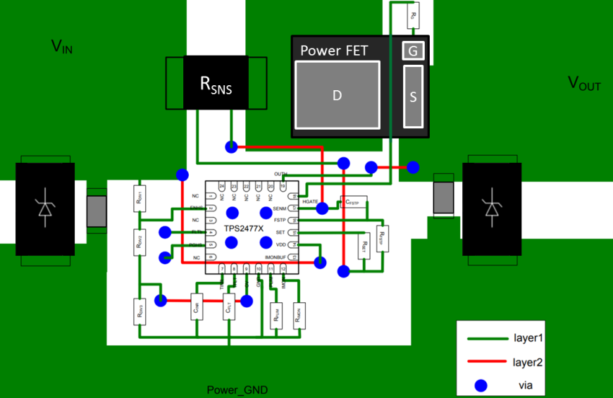
One subset of power ICs that has seen significant innovation in recent years is the hot-swap controller. Historically, external metal-oxide semiconductor field-effect transistor (MOSFET) hot-swap controllers have been a very popular power-path protection solution. However, the footprint for such a solution can be quite large given the need for an external sense resistor and power MOSFET. As shown in Figure 1, a hot-swap solution can take up a significant amount of board space.

Figure 1: An external MOSFET solution with the TPS2477x hot-swap controller

Decreasing the package size of these ICs will increase the RON, which will worsen the power performance. However, with TI’s proprietary processes, it is possible to optimize both parameters and achieve superior power density in a very small footprint. Figure 2 shows the TPS25982– a new 24-V, 15-A eFuse that comes in a 4-mm-by-4-mm package.

Figure 2: TPS25982 (center) and TPS2595 (right) size comparison

For even smaller footprint solutions, the TPS2595 eFuse comes in a 2mm x 2mm package and for higher voltages, the TPS1663 eFuse supports up to 60V, as shown below in Table 1.

Device

Voltage

Current

RON

Package

TPS25982

2.7 V-24 V

15 A

3 mΩ

4-mm-by-4-mm quad flat no-lead (QFN)

TPS2595

2.7 V-18 V

4 A

34 mΩ

2-mm-by-2mm QFN

TPS1663

4.5 V-60 V

6 A

31 mΩ

4-mm-by-4mm QFN

Table 1: Texas Instruments eFuse options

As overall power demands increase in the market, board space becomes more and more valuable. As a result, optimizing power efficient solutions in a small footprint will be something all power designers will have to consider. 

Deciphering low Iq: Using WEBENCH® to design near 100% duty-cycle for ultra-low power applications

$
0
0

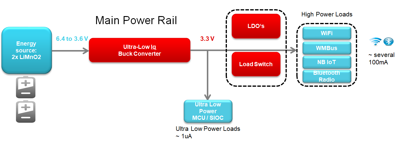
Many battery-powered applications require a step-down buck converter to work in 100% duty-cycle, where VIN is close to VOUT, in order to extend battery run time when battery voltage is at its lowest value. For example, let’s say that there are two lithium manganese dioxide (Li-MnO2) batteries powering a smart meter. Li-MnO2 batteries are primary non-rechargeable cells used increasingly in smart gas or water meters because of their long operational lives (as much as 20 years) while being more cost-effective than lithium thionyl chloride batteries. Figure 1 shows the system configuration of two Li-MnO2 cells placed in series (2s1p) and then stepped down to power a microcontroller.

A smart meter power architecture

Figure 1: A smart meter power architecture

Ultra-low quiescent current (IQ) DC/DC converters can help you design applications with a battery lifetime up to 20 years. The load profile of a smart meter application is not a continuous load but a variable load profile. In order to enable long battery life, the system will draw a high current only occasionally (to send a wireless signal or actuate a valve), and then go back to a very low load condition. This type of load profile enables low average current consumption in the microampere range. High efficiency at such light loads requires ultra-low IQ, especially during the off-time where current consumption could be much lower than the average current consumption.  TI’s TPS62840 ultra-low power buck converter has an operating IQ of only 60 nA and can regulate a 3.3-V power rail. The TPS62840’s very low IQ in 100% mode – 150 nA – further extends battery run time.

To better help you design and simulate your ultra-low power-supply circuit, WEBENCH® Power Designer is an online tool that enables the creation of customized power supply designs based on your specifications.

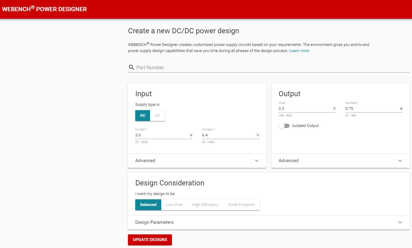
In our example, the average voltage per cell is around 3.0 V. The initial voltage of a cell is approximately 3.2 V when fresh, and the voltage can drop to less than 2 V when fully discharged. Assuming that each battery discharges down to 1.8 V and is 3.2 V when fresh, enter these parameters into WEBENCH Power Designer (Figure 2).

Design specification entered in WEBENCH Power Designer

Figure 2: Design specification entered in WEBENCH Power Designer

Using a 3.6-V minimum input voltage in the WEBENCH Power Designer search tool yields 51 possible devices, but the TPS62840 is not one of them. Why is that?

WEBENCH focuses on two initial parameters to help you find the best device for your system:

1. VINMIN> VOUT is the first check WEBENCH Power Designer looks for in the user inputs for buck converters topologies. If VINMIN > VOUT, then WEBENCH Power Designer selects buck converters as part of the solutions list. If VINMIN≤ VOUT, WEBENCH Power Designer recommends buck-boost converters to regulate your VOUT instead of buck converters that operate in 100% Duty Cycle mode. This is because WEBENCH wants to give you a solution where your VOUT is regulated even when VINMIN ≤ VOUT.

2. After passing the first check, the second check verifies if the calculated duty cycle is greater than the max duty cycle specified in the buck converter datasheet. For buck converters that can operate in 100% duty cycle mode, 99.9% is used as the threshold. Losses are included when calculating the duty cycle. This increases the calculated duty cycle in WEBENCH Power Designer far above the ideal VOUT/VIN.

After selecting numerous devices, WEBENCH Power Designer performs detailed designs for each device. Below are three different outcomes which can be observed depending on the input parameters used:

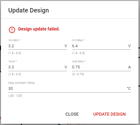
  • VIN from 3.2 V to 6.4 V, IOUT_MAX = 0.75 A and VOUT = 3.3 V in the TPS62840 WEBENCH Power Designer model (Figure 3).

Error message that the input voltage is too low

Figure 3: Error message that the input voltage is too low

The design update is failing because the minimum VIN is lower than VOUT. This design does not pass WEBENCH’s first check.

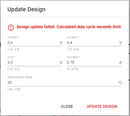
  • VIN from 3.6 V to 6.4 V, IOUT_MAX = 0.75 A and VOUT = 3.3 V in the TPS62840 WEBENCH Power Designer model (Figure 4).

Error message that the duty cycle is too high

Figure 4: Error message that the duty cycle is too high

The design does not update because the duty cycle when calculated includes losses such as the high-side MOSFET RDSON and inductor DCR. Here, the duty-cycle value is greater than 99.9%. This design does not pass WEBENCH’s second check.

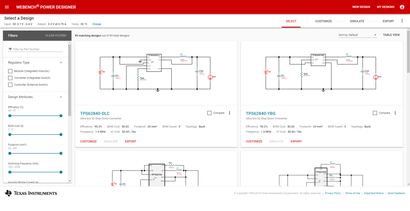
  • VIN from 3.7 V to 6.4 V, IOUT_MAX = 0.75 A and VOUT = 3.3 V on the WEBENCH Power Designer Select a Design screen (Figure 5).

The TPS62840 displayed in WEBENCH Power Designer

Figure 5: The TPS62840 displayed in WEBENCH Power Designer

The final example displays the TPS62840 since the design passed both checks.

Tips to use WEBENCH Power Designer more effectively when close to 100% duty-cycle:

  • Add a sufficient delta between the input voltage and the output voltage to reduce the duty cycle.
  • Reduce the output current to reduce losses and reduce the duty cycle.

Either of these solutions enable WEBENCH Power Designer to design with the TPS62840. In an actual application, operating in 100% mode is normal and generally acceptable in order to fully discharge the battery. In 100% mode, the output voltage of a step-down converter decreases as the battery voltage decreases. This can still fit the system specifications of most loads.

Additional resources

Do all rails need low Iq?

$
0
0

a smart meter

All designers of ultra-low power systems are concerned about battery life. How much time will elapse before the battery in a fitness tracker will need recharging? Or, for primary cell systems, how long will it be before a technician must service the smart meter and change the battery? Clearly, the design goal is maximum battery runtime. For a fitness tracker, a week of runtime may be good, but a smart meter operates for 20 years or more. What do you need to consider in each of the various subsystems to achieve this runtime?

In many systems, one or two voltage rails are always enabled. These power the system microcontroller (MCU), a critical sensor or maybe a communication bus. These always-on rails need to have very high efficiency to extend the battery runtime. A good subsystem design reduces the current drawn by each of the always-on subsystems to a minimum – many times this is less than 10 µA, or even 1 µA, total. As I discussed in this technical article, an ultra-low power supply is required to reap the benefits of these subsystem optimizations. In rails with very low current consumption, this translates to a power supply with ultra-low quiescent current (IQ), such as the 60 nA IQTPS62840.

You might be tempted to think that it’s most important to minimize the current consumption of each of the power supplies while they are running. Reducing the IQ increases efficiency and thus extends the battery runtime by consuming less battery power. But is the efficiency increase always significant? For systems that operate at relatively higher load currents, such as displays and some sensors, the answer is clearly no; the output power is much greater than the IQ power. For example, if the display in a fitness tracker draws 12 V at 5 mA (60mW total), the 100µA IQ drawn from the 3.6V battery (0.36 mW total) is insignificant.

More important for these types of subsystems is the power consumption when disabled. An ultra-low power system turns off power-hungry subsystems most of the time in order to conserve the battery. Thus, the shutdown current becomes critical to the system’s battery life. This leakage current, as it is frequently called, may be so high that you will have to add a load switch to disconnect the subsystem from its power source to further reduce its shutdown current. The TPS62748, high efficiency buck converter, provides both a load switch and 360 nA ultra-low IQ for such systems.

When a load switch is not used, you must consider both the leakage current into the device itself and its load if there is a path to the load through the device. This is frequently the case with a boost converter, so specific circuitry is sometimes added to break this path, such as the isolation switch in the TPS61046, boost converter. In other cases, this path is specifically optimized to allow bypass operation – powering the load with less than 50 nA of shutdown current consumption in the disabled device.

It’s important to pick the right type of device – ultra-low IQ or ultra-low shutdown current – for your specific subsystem. These nuances are prevalent in every ultra-low power system, from a wearable to a smart meter to a medical device, so consider the requirements of your application wisely before choosing the optimal solution. 

Additional Resources:

Layout matters: solving pinout assignment issues for DC/DC converters in WCSP packages

$
0
0

The miniaturization trend in consumer electronics has taken hold for good. Consumers are demanding smaller electronics with better features: more flash capacity in solid-state drives, faster smartphones, more integrated communication modules, etc. To achieve this, engineers must look for increasingly power dense solutions. One challenge associated with achieving a high-power-density solution is finding small DC/DC converters with compact external components. When it comes to size, DC/DC converters in wafer chip-scale packages (WCSPs) are smaller than standard quad flat no-lead (QFN) or small-outline transistor (SOT) packages. WCSPs have also lower height than QFN or SOT packages, which can help engineers design not only smaller equipment but also one with a lower profile.

The trouble with logic signal pins

Although DC/DC converters in WCSP have the size advantage, the pinout assignment of a typical WCSP might prevent engineers from choosing this package. Often, some logic signal pins (like the EN pin or the SDA and SCL pins of the I2C interface) sit in the middle of the package because other pins with higher priorities in silicon layout (like VIN, AVIN, AGND, PGND and the output sense pins) must connect to the signal traces directly. Because external components should be placed as close to these pins as possible, engineers have to insert small vias for the pins in the middle of the package to achieve proper signal routing during printed circuit board (PCB) layout.

In order to fit in more features (which equals more pins) in one device, engineers increasingly opt for a smaller WCSP pin pitch. While the 0.5-mm or 0.4-mm pitch was used in old devices, nowadays the 0.35-mm pitch is being adopted by many new devices in the market. Once the WCSP pin pitch is 0.35 mm, traditional PCB manufacturing prevents engineers from placing vias in the middle of the package. To address this issue, engineers have to either do away with vias altogether or use an advanced PCB assembly technology, which raises the cost of the overall solution. As a result, engineers have to choose between a larger solution size or a less competitive product.

To address this problem, engineers should consider the pinout assignment when choosing the right buck converters in WSPC for their solutions. TI’s TPS62866 is a 6-A synchronous step-down converter which measures only 1.05x1.75x0.5-mm in WCSP. For the same current level buck converters in QFN, the typical package size is 3x3x1-mm. Figure 1 shows the pinout assignment and typical PCB layout of the TPS62866.


Figure 1: Pinout of the TPS62866 with a typical PCB layout

The absence of logic pins in the middle of the integrated circuit means that engineers don’t need special vias for PCB routing, even though the pin pitch is 0.35 mm. Such assignment makes it also possible to place all signal traces around the device for direct routing, further saving board space and allowing engineers to shrink the overall power supply solution, leaving more room for the features that consumers crave.

A reasonable pinout assignment is an important feature for DC/DC converters in WCSP packages. The TPS62866 provides a good pinout assignment and implements many features including I2C interface in a 1.05x1.75x0.5-mm, 0.35-mm pitch WCSP.

Additional Resources

How to avoid the pain of a discharged device

$
0
0

Frustration caused by a dead mobile device battery is not limited to adults with phones. Children too young to read can transform from charming angels to noisy demons when their tablet battery dies.

This can be especially painful when it occurs during a long car ride. I have seen this happen, and recommend taking all reasonable steps to avoid it.

How did we get here?

Before mobile devices, automotive cigarette lighters were populated with cigarette lighters, and sometimes radar detectors or CB radios. These sockets provide considerable power and are typically fused at 15 A or 20 A. Today they are commonly occupied by an adapter for charging mobile devices. Almost all of these adapters have one or more USB ports as an output.

More recently, automakers have been integrating USB charge ports into vehicles at the factory. These USB ports are either in the head unit (aka the radio), the console, or in a rear-seat charging hub. Initially, automakers installed only one or two ports and each port only had to supply 1.0-1.5 A. The DC/DC converter used to create 5 V for these ports had to deliver a modest 5-15 W, and a reasonably thoughtful thermal design could provide reliable operation.

Such is not the case today.

As mobile devices and USB evolved, charging current demands increased to 2 A, then 2.4 A, and now, with USB Type-C™, each port may require 3 A. This significant growth in USB power demand has driven many automakers to move USB charging power conversion and management out of the head unit and into hubs or consoles. This allows greater thermal, mechanical and electrical design flexibility than a location in the head unit.

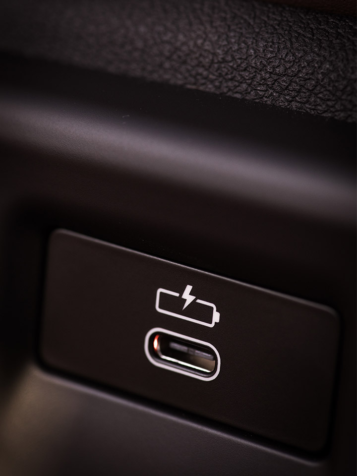
Figure 1: Typical Console USB Port

Getting integrated with the TPS25830-Q1 and TPS25831-Q1

A complete charge port design includes compliance with power, performance, safety and self-protection standards. Some of these standards require:

  • A wide input voltage (VIN) DC/DC converter to provide 5 V at up to 3 A with 8 V < VIN< 40 V.
  • A current-limiting USB power switch to prevent excessive current in an overload condition.
  • Electrostatic discharge protection for sensitive circuitry.
  • Short-to-battery/ground protection to protect data and power against connector pin mishaps.
  • USB charge port control – USB Battery Charging (BC) Revision 1.2 and/or USB Type-C handshake capability to enable the maximum charging current.

Historically, this required multichip solutions, but today it is possible to satisfy all of these functions with a single 5-mm-by-5mm 32-pin quad flat no-lead device that has 94% efficiency at a 12-V VIN. The TPS25830-Q1 and TPS25831-Q1 USB charge port converters are simple to use and integrate a DC/DC converter to minimize solution size and cost.

These devices enable maximum charging rates in divider mode and BC1.2 devices, along with USB Type-C handshaking. Cable compensation counteracts voltage droop across USB cables and provides 5 V at the USB connector over the full range of load current.

Smart thermal management on the TPS25831-Q1 prevents thermal shutdown due to overheating by progressively reducing load current as the system temperature approaches the overtemperature threshold.


Figure 2: Equivalent functions of TPS25830-Q1 and TPS25831-Q1 devices

If your automotive USB charge port design calls for high efficiency and small size – and low noise from back-seat occupants – check out the TPS25830-Q1 and TPS25831-Q1 and order an evaluation module today.

Additional resources


Overcoming design challenges for low quiescent current in small, battery-powered devices

$
0
0

This post was written in conjunction with Manuel Diaz Corrada

Thanks to advances in miniaturization, Bluetooth® communication and embedded processing, modern hearing aids have more features than ever, from streaming music to being able to adjust hearing amplification from an app on your smartphone.

These increased capabilities come at a price, however: modern features require more power. Increased power consumption is a challenge for engineers designing hearing aids, primarily because older versions use disposable zinc air batteries. These batteries typically last about two weeks. But when you add more features to hearing aids, such as giving them the ability to play music, the battery life could drop down to hours. Thus, engineers are using rechargeable lithium batteries in their next-generation hearing aid designs.

Rechargeable lithium batteries increase the power system complexity in a variety of ways, the most important being how to safely and accurately charge the battery. There are also extra design considerations when using two hearing aids. Because the left and right earpieces have no physical connection, it is not possible to charge both of them through a single cable simultaneously. So almost all new hearing aids are now equipped with a case that has both charging and storage functions.

This case is designed with specific sockets for each earpiece to ensure proper charging. The charging for the earpieces must be precise, since rechargeable hearing aids are typically 25 mAh-75 mAh and the charging case ranges from 300 mAh-70 0mAh. This translates to about 24 hours of usage for the earpieces and about 10 recharge cycles from the case, before the case itself needs to be re-charged.

With a charging case, hearing aid designers now have three different lithium batteries to consider: one for the case and two for the earpieces. The choice of battery chargers plays a significant role in the design.

It is also critical to note that charging a battery from a battery (i.e. charging the earpiece battery from the charging case battery) is not as simple as charging from the wall, since the voltage difference between the two batteries will not be very large. There has to be internal circuitry to boost the voltage difference between the charging case and the earpieces to enable full charging. As the battery discharges, its voltage is slowly dropping. Looking at the discharge curve shown in Figure 1, at around 50% of battery capacity, the charging case voltage would be at around 3.6 V. But that means that without a boost, the charging case can only charge the earpieces up to 3.6 V, even when the energy stored in the case is sufficient to charge them fully.

Figure 1: A sample battery discharge curve for a lithium-ion battery; the typical mean point voltage is 3.6 V and the end-of-discharge voltage is 3 V (Source: “Characteristics of Rechargeable Batteries”)

In such a scenario, most engineers would think to use a discreet boost. While a discreet boost does work, it typically increases solution size and inefficiencies by adding an additional boost and inductor component to the power architecture.

To overcome these challenges, consider on-the-go charging supported by quiescent currents. For example, TI’s BQ25619 battery charger and BQ25155 linear charger support charging without an external boost. In the hearing aid application, you could place the BQ25619 in the charging case and the BQ25155 within each earpiece.

Then, instead of always boosting the charging case output to 5 V, you would instead boost to the minimum voltage necessary to allow sufficient headroom between the charging case and earpiece batteries using the BQ25619’s boost functionality. This reduces the power loss of unnecessary boosting and also increases earpiece charging efficiency, since the voltage differences are reduced.

The BQ25155 is a good fit for the earpieces, since its 3.4-V input voltage minimum allows longer charging without the boost, and its 43-µA quiescent current increases battery run time. Meanwhile, the BQ25619’s 7-µA quiescent current in ship mode maximizes charging case shelf life. The BQ25619’s 20-mA charge termination current enables it to charge small-sized batteries with 7% more capacity.

The good news is that these benefits are not limited to hearing aids: all two-battery device systems, including earbuds and wearable patches, can benefit from these innovations. TI will continue to implement two-charger configuration in future designs with features like:

  • Higher efficiency charging for both the earpieces and charging case while providing battery monitoring and protection, and reducing the total bill of materials with an integrated boost.
  • Pin reduction for earpieces and charging cases by requiring only one line of communication.

With the BQ25619 and the BQ25155, you can improve the amount of charge cycles that are extractable from a charging case without increasing cost or solution size.

Additional resources

Understanding the difference between capacitors, capacitance and capacitive drop power supplies

$
0
0

Knowing the difference between a capacitor’s rated value and its actual capacitance is key to ensuring a reliable design. This is especially true when considering high-voltage capacitors used in capacitive drop power supplies for equipment like electricity meters, since losing too much actual capacitance may result in insufficient power to support the application.

With a capacitive drop power supply, the high-voltage capacitor is typically the largest (and one of the more expensive) components in the circuit. When sizing capacitors, it is essential that the actual capacitance can support the load current that the design requires.

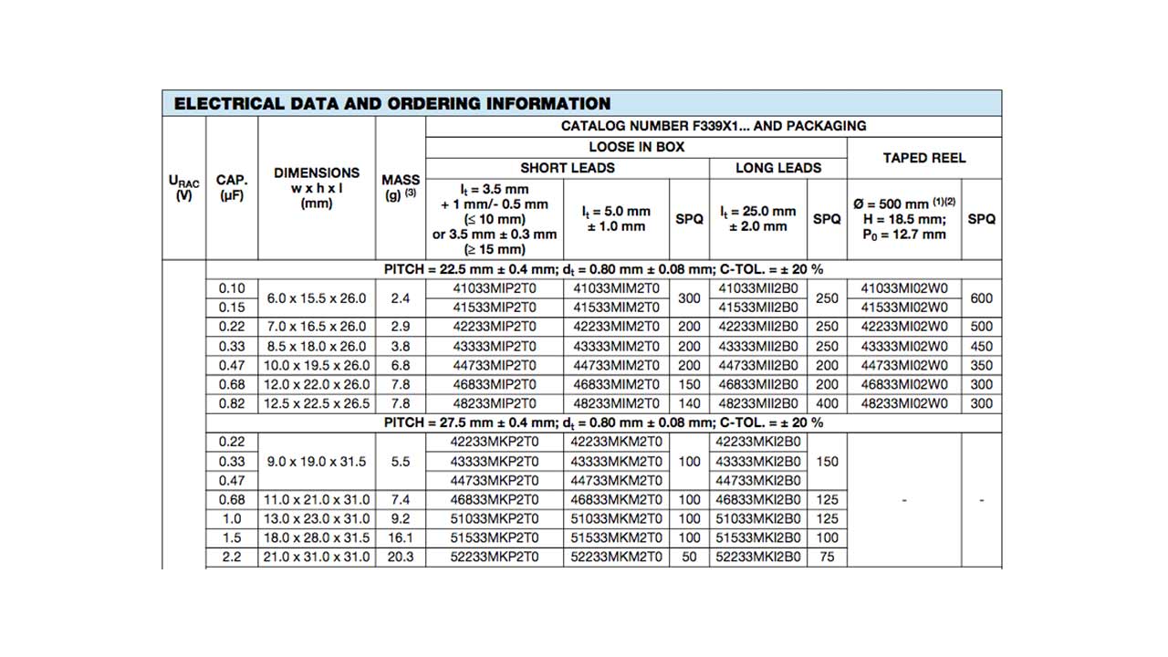
Figure 1 shows the existing capacitance values of capacitors available from a capacitor manufacturer, Vishay. Let’s assume that your design calculations show that your design requires a 1-µF capacitor (90 VAC_RMS at 60 Hz and 5 VOUT @ 25 mA). Considering the available capacitors, you might choose a 1.2-µF capacitor to accommodate the manufacturer’s tolerance of 20%. However, taking into consideration the capacitor’s tolerance and aging effects, you may see a 50% reduction in the actual capacitance of your capacitor over time. In other words, in the worst-case scenario, the 1.2-µF capacitor you chose may only have 0.6 µF of capacitance at its end of life. 

 Figure 1: Sample range of high-voltage capacitors available from manufacturer Vishay

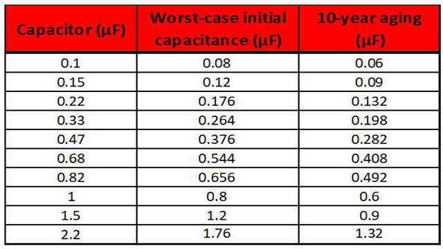
Wait, aging is an issue? If the application is expected to work for 10-plus years, it is not unreasonable to assume that film capacitors may lose ~25% of their capacitance over the lifetime of the product, due to operating temperature, load current and humidity. Table 1 shows a prediction of the total capacitance after considering worst-case tolerance and aging.

Table 1: Tolerance and aging effects on actual capacitance

Considering the effects of the tolerances, the best choice to support a 25-mA load at 5 VOUT in a traditional capacitive drop architecture, is a 2.2-µF capacitor, which comes with serious size implications. Is there a better way?

One way to mitigate the effects of capacitance loss due to aging is to simply use a lower-value capacitor. For example, if you used a step-down converter to reduce a DC-rectified 20 V down to 5 V, with perfect efficiency you could maintain 25 mA at the 5-V output, but you would only need to size the high-voltage capacitor to support 6.25 mA. To clarify – in the above example, if a linear power solution required 1 µF, a four-time reduction in voltage will yield a four-time increase in load current capability. In this example, 1 µF reduces to 0.25 µF.

Looking at the same derating for tolerance, you would calculate the need for a 0.3-µF capacitor, yet the next available capacitor has a value is 0.33 µF. Add to that the aging effects, and the next available capacitor you should consider is actually 0.47 µF.

The only problem with using a DC/DC step down converter in applications like electricity meters is that they tend to require a very high level of tamper immunity. This means preventing external magnetic fields from impacting the design’s additional circuitry like Hall-Effect sensors or a tamper-proof enclosure is required, which will add additional cost.

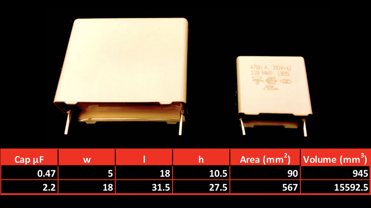
One way to resolve the issue of the oversized capacitor and still support tamper immunity is to use a nonmagnetic step-down converter. TI’s TPS7A78 voltage regulator requires no transformers or inductors to produce a nonisolated low-voltage output. The TPS7A78 reduces a 2.2-µF capacitor to 0.470 mF, guaranteeing 25 mA of load current over the life of the product. Figure 2 compares the area and volume of the two capacitors.

Figure 2: Area and volume comparison of two high-voltage capacitors

So why do smaller capacitors matter? The obvious answer is the overall solution size. But the less obvious benefits are standby power and efficiency. Reducing the amount of capacitance required by four times reduces standby power from ~300 mW down to ~77 mW. Adding the intelligent clamp circuit behind the TPS7A78 supporting a 25-mA load cuts down the total standby power to ~15 mW.

Knowing how to minimize the capacitor to ensure enough capacitance saves cost for both the manufacturer and the consumer when using capacitive drop power supplies.

Additional resources

Options for reducing the MLCC count for DC/DC switching regulators

$
0
0

Multilayer ceramic capacitors (MLCCs) are popular in electronic circuits, particularly for decoupling power supplies, but have become harder to procure due to a severe market shortage of MLCCs in larger case sizes, which began in 2018. Market indicators show that nothing will change until at least 2020. Consequently, designers are now seeking ways to reduce the number of MLCCs in DC/DC switching regulators.

One option to minimize the MLCC count for DC/DC switching regulators is to select a device capable of operating with fewer external capacitors. Another option is to choose a DC/DC switching regulator with TI’s D-CAP+™ control mode. Increasing the switching frequency will also help reduce capacitor count. For example, increasing the switching frequency of the TPS563201 from 580 kHz to 1.4 MHz led to the design of the TPS563249, which has one less capacitor.

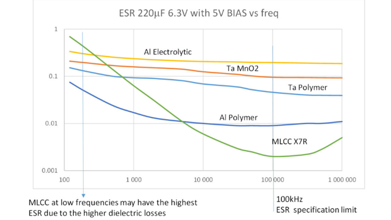
The option for reducing the MLCC count for DC/DC regulators studied in this article considers the use of a replacement technology. The most common types of replacement technologies are film, aluminum (liquid and polymer), and tantalum (solid and polymer). There are pros and cons of each technology, including their capacitance, voltage range, equivalent series resistance (ESR), size, and current rating. When selecting capacitors for DC/DC switching regulators, ESR is usually the biggest differentiating factor because the higher it is the more output-voltage ripple, heating, and input noise occur, which is why MLCCs are popular for DC/DC switching regulators since they most often have the lowest ESR. Aluminum polymer capacitors share several characteristics with MLCCs and have a low enough ESR to be a replacement for MLCCs amongst designers. As you can see in Figure 1, aluminum polymer capacitors are the type of capacitors that have the closest ESR values to MLCCs.


Figure 1: ESR of various capacitor technologies (source: Why low ESR matters in capacitor design)

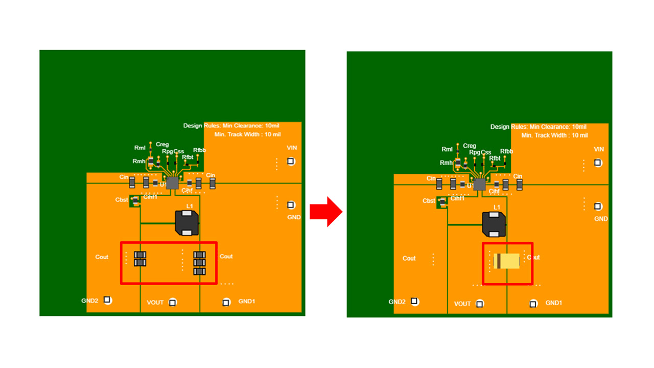
One downside of aluminum polymer capacitors is that they are bigger than MLCCs. When using the WEBENCH® Power Designer tool, which provides printed circuit board (PCB) layout information, you can see in Figure 2 that if you replace the five output MLLCs of the TPS568215 synchronous buck converter with one aluminum polymer capacitor, both solutions occupy similar surface areas.

Figure 2: Replacing MLCCs with an aluminum polymer capacitor for the TPS568215 in the WEBENCH Power Designer tool

The question now comes down to performance. How do aluminum polymer capacitors compare to MLCCs, and can they truly replace MLCCs without forcing designers to make too many compromises?

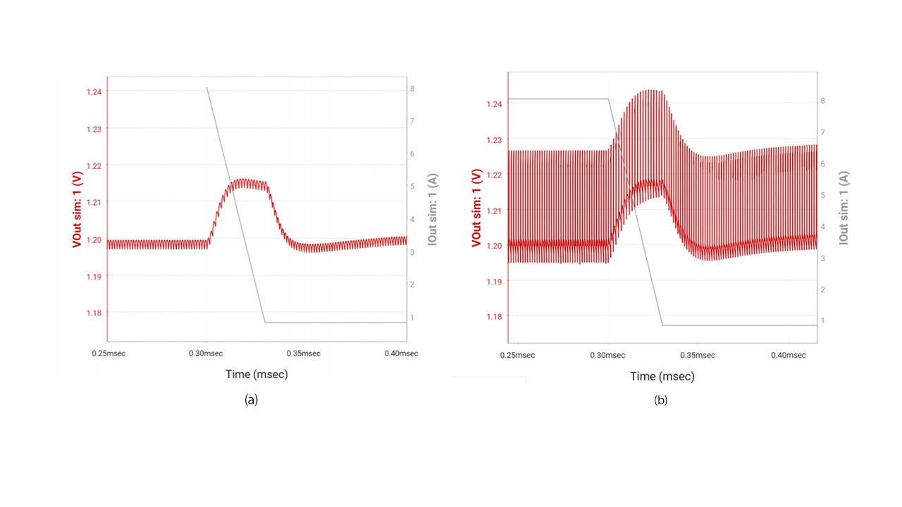
To get a rough idea, I used the WEBENCH Power Designer tool to simulate some load transient responses. As shown in Figure 3, using an aluminum polymer capacitor at the output instead of the MLCCs increases the output voltage ripple tenfold. Thus, replacing MLCCs with only aluminum polymer capacitors is not a feasible option if you need decent performance.

Figure 3: Load transient simulations run on the WEBENCH Power Designer tool for the TPS568215 with output MLCCs (a); and aluminum polymer capacitors (b)

What about combining MLCCs and aluminum polymer capacitors to help reduce the voltage ripple while minimizing the ceramic count on DC/DC switching regulators? To determine that, I performed some real PCB testing with the TPS568215 evaluation module (EVM). The strategy was first to run some tests on the initial configuration of the EVM to validate the test setup by comparing the input voltage ripple, output voltage ripple, load transient response, start up response, and shut down response with the ones from the datasheet. Then, I tried out different capacitor configurations both at the input and output of the EVM.

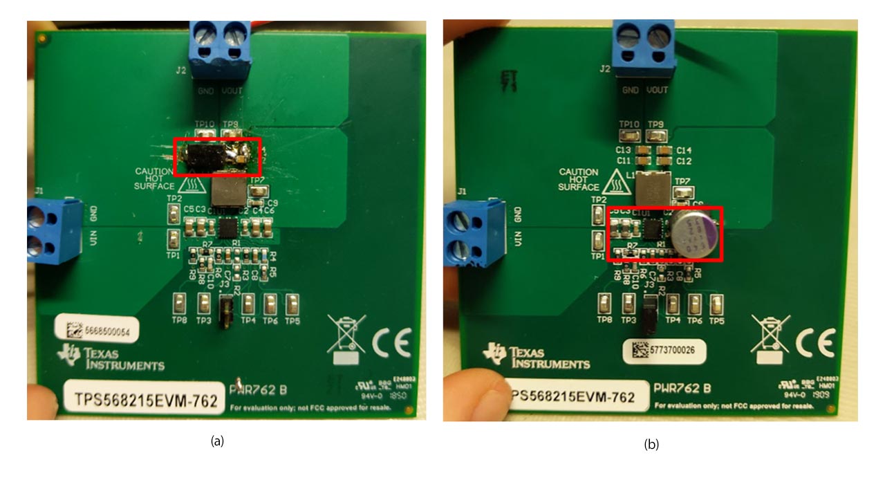
The two setups that showed the closest results to the initial configuration were using a mix of aluminum polymer capacitors and MLCCs, as shown in Figure 4, where the setup in Figure 4a tested the output voltage ripple and the setup in Figure 4b tested the input voltage ripple.

Figure 4: TPS518215EVM setup with one aluminum polymer capacitor in parallel with one MLCC at the output (a); one aluminum polymer capacitor in parallel with three MLCCs at the input (b)

The tests were performed with a 12-V input and an 8-A load. It was not surprising to see an increase in voltage ripple for both the input and output, but a smaller one than when using only aluminum polymer capacitors. The output voltage ripple went from 8 mV to 14 mV, as you can see in Figure 5, while the input voltage ripple went from 13 mV to 24 mV, as you can see in Figure 6.

Looking at the ESR values of the original capacitor configuration versus the hybrid configuration explains why this occurred. For the input setup, the total ESR when using four MLCCs in parallel is 0.57 mΩ, while it is 1.08 mΩ when using two MLCCs in parallel with one aluminum polymer capacitor. For the output setup, the total ESR when using four MLCCs in parallel is 1.05 mΩ, while it is 1.57 mΩ when using one MLCC in parallel with one aluminum polymer capacitor.

Figure 5: Output voltage ripple of the TPS518215EVM with four MLCCs in parallel (a); one aluminum polymer capacitor in parallel with one MLCC (b)


Figure 6: Input voltage ripple of the TPS518215EVM with six MLCCs in parallel (a); one aluminum polymer capacitor in parallel with three MLCCs (b)

As I’ve shown in this article, one way to reduce the count of MLCCs for DC/DC switching regulators is to replace some of them with aluminum polymer capacitors. Needless to say, you will need further tests to check that the performance of this hybrid capacitor configuration still fits within your design requirements. Every capacitor has its own characteristics and every design has its own requirements, but this alternative is definitely something to keep in mind while MLCCs are in short supply.
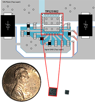
Additional Resources:

Tips for making your embedded system’s power rail design smaller

$
0
0

Achieving a small power rail solution size is one of the highest priorities for embedded system engineers, especially for those designing industrial and communications equipment such as drones or routers. Compared to models released a few years ago, currently available drones are much lighter and have smaller fuselages, while routers are now more portable and compact with a built-in power adapter. As equipment size shrinks, engineers are looking for ways to shrink the power supply solution. In this technical article, I’ll provide a few tips to help you make your power rail design smaller, while demonstrating how to resolve the resulting thermal performance challenges.

Shrinking the package

One obvious way to reduce your solution size is to choose an integrated circuit (IC) in a smaller package. Small-outline (SO)-8 and small-outline transistor (SOT)-23-6 packages are common for 12-V voltage rail DC/DC converters. They are typically very reliable. However, if you work in an industry where every millimeter counts – such as the drone market – you may be looking for an even smaller DC/DC converter. The SOT-563 package is almost 260% smaller than the SOT-23-6, and 700% smaller than the SO-8 package. Figure 1 compares the size of the mechanical outline of all three packages.

Figure 1: Mechanical outline sizes of three converter packages

Apart from choosing a smaller package, another approach to reducing your solution size is to reduce the output inductor and capacitor. Equations 1 and 2 calculate the output inductance (LOUT) and output capacitance (COUT)


where ris defined as the ratio of current ripple of inductor, VRIPPLE is the maximum allowed peak-to-peak ripple voltage and fsw is the switching frequency of the converter. Because LOUT and COUT are both inversely proportional to fsw, the larger the switching frequency, the smaller the LOUT and COUT.  Smaller inductance or capacitance means engineers can select an inductor or a capacitor of a smaller size. Converters with a higher fsw can work with these smaller inductors and capacitors.

Addressing thermal performance

A smaller system faces more significant thermal performance issues, given the limited path for heat dissipation. To effectively solve any possible thermal issues and achieve higher efficiency, you can apply converter switches with a lower RDS(on). Equation 3 calculates the temperature rise on a DC/DC converter:

where PLOSS is the total power loss of the converter and RΘJA is the junction-to-ambient thermal resistance.Consider a 2-A load converter with an average RDS(on) change from 100 mΩ to 50 mΩ. The power loss of this device will result in a 200-mW decrease, which will bring a 16°C cooldown on a typical SOT-563 board with a thermal resistance of 80°C/W. Therefore converters with a lower RDS(on) offer better working conditions at a lower temperature.

Turning theory to practice

A real-world embedded system often applies multiple step-down DC/DC rails. Figure 2 shows a block diagram of a home router power-stage architecture that needs four lower voltage rails. Let’s take three typical devices applied in this type of system to demonstrate how package size and switching frequency affect power rail solution size.

Figure 2: Power-stage architecture of an embedded system
 
The TPS54228 has a 700-kHz frequency in an SO-8 package. The TPS562201 has a 580-kHz frequency in an SOT-23-6 package, and the TPS562231 has a 850-kHz frequency in an SOT-563 package. The TPS562231 has the highest frequency and the smallest IC package size. This solution size is about 142% smaller than the TPS562201, and 227% smaller than the TPS54228, as illustrated in Figure 3.

 
Figure 3: Solution sizes of converters with different packages
 
The RDS(on) of the integrated metal-oxide semiconductor field-effect transistor (MOSFET) in the TPS562231 is 95 mΩ (high side) and 55 mΩ (low side). Figure 4 is a thermal image of the full load temperature rise of a 12-V input on the TPS562231 evaluation board.

 
Figure 4: Thermal image of the TPS562231 with a 12-V input voltage
  
In general, the TPS562231 works in an 850-kHz switching frequency sealed in a small SOT-563 package, which can help reduce the overall solution size. Its low on-resistance also allows for good thermal performance. It’s suitable for routers, drones, set-top boxes or any other embedded designs that require small solution sizes.
 
Additional resources


Using low-Iq voltage supervisors to extend battery life in handheld electronics

$
0
0

As electronics become more portable, the need for high-accuracy integrated circuits with a small footprint and low quiescent current (IQ) increases. To monitor key voltage rails in handheld electronics such as electric toothbrushes and personal shavers, design engineers typically choose a simple voltage supervisor and look for devices that enable a small solution size and low IQ to improve battery life. However, in the past, optimizing a system often involved a trade-off between space, low IQ and accuracy.

The generic electric toothbrush diagram shown in Figure 1 highlights the internal complexity of a simple handheld product and how the subsystems connect together in such a compact device. Similarly, personal shavers share subsystems that call for the same design needs including low IQ, high-accuracy, and compact size.

Figure 1: Electric toothbrush block diagram

Benefits of low IQ and small size for battery operated devices

In personal electronics such as electric toothbrushes and personal shavers, devices with low IQ could save hours of total battery life. In addition, accurate sensing of the voltage ensures battery is used to its full capacity. Since battery-operated devices are often hand held, this puts space constraints on the electronic components.

A simple voltage supervisor to monitor a single voltage such as a battery needs only three pins – sensed voltage, ground and output, which indicates if the sensed voltage is above or below a chosen threshold. Such simple voltage supervisors are often offered in industry-common three pin small outline transistor (SOT)-23 packages. One example is the TPS3836 - a voltage supervisor (reset IC) with a low IQ of 220 nA available in a SOT-23 package.

However, at 2.9 mm x 1.5 mm, the size of a typical SOT-23 package is often too big for a small battery-operated device. A possible solution is to use an even smaller package such as the extra small outline no-lead (X2SON) package, which measures only 1.0 mm by 1.0 mm and is a quarter of the size of the three-pin SOT-23 package. Engineers looking for a package that’s easy to mount and inspect might prefer one with visible pins, such as a three-pin SC-70 package that measures 2.0 mm by 1.25 mm and is a third smaller than the three-pin SOT-23 package.

The TLV809E comes in a SC-70 package, which allows engineers to considerably shrink the size of their solution when compared with similar devices such as LM809 or TLV809. This small, yet easy to mount package with visible pins can serve a wide breadth of handheld electronics applications.

Another important characteristic for device startup: VPOR

The power-on-reset voltage (VPOR) represents the minimum input voltage (VDD) required for a controlled output state. To maximize the battery capacity and still have reliable device operation, the VPOR voltage should be as low as possible. The TLV803E and TLV809E can achieve a VPOR of 700 mV, which minimizes the range of undefined output and ensures operation to the maximum possible battery capacity.

As engineers design personal devices that are more compact but require more features and increased performance, it is important to think about ways to improve battery life, obtain low IQ and maintain high-accuracy voltage supervision. The TLV803E and TLV809E voltage supervisors provide flexible and powerful monitoring solutions for compact battery-powered devices such as electric toothbrushes and personal shavers.

Additional resources


Viewing all 437 articles
Browse latest View live


<script src="https://jsc.adskeeper.com/r/s/rssing.com.1596347.js" async> </script>