Quantcast
Channel: Power management
Viewing all 437 articles
Browse latest View live

Is there a universal tool for DC/DC voltage conversion?

$
0
0

Most applications or subcircuits require a constant voltage supply within a certain voltage tolerance window in order to operate properly. Battery-driven applications such as wireless sensors and personal handheld devices need voltage conversion to generate the required output voltages while the battery discharges and reduces its voltage. Applications supplied by a fixed rail such as optical modules, wired sensors, or active cables or dongles might also need voltage conversion if the available rails do not fit the required input voltage, or if the voltage variation exceeds the required tolerance window.

In this article, I will show how a buck-boost converter might be a good solution for voltage conversion, and whether it might even be a universal tool for any type of DC/DC voltage conversion.

When to use a buck-boost converter

Typically, if the available supply voltage for a circuit or subcircuit is lower than the required voltage, a boost (step-up) converter efficiently converts DC voltages to a higher voltage level. If the available supply voltage is higher than the required voltage, a buck (step-down) converter performs the voltage conversion.

To be able to accept supply voltage ranges that are both higher and lower than the required output voltage, you need a buck-boost converter. A buck-boost converter is a hybrid of a buck and a boost converter, which becomes clearer when looking at its block diagram, shown in Figure 1.

Figure 1: Buck-boost converter block diagram

By merging the architecture of a buck converter (shown in green in Figure 1) with the architecture of a boost converter (shown in orange in Figure 1), a buck-boost converter can both step up and step down the output voltage. Depending on the actual input voltage and programmed output voltage, the control loop determines whether the device needs to operate in buck or boost mode.

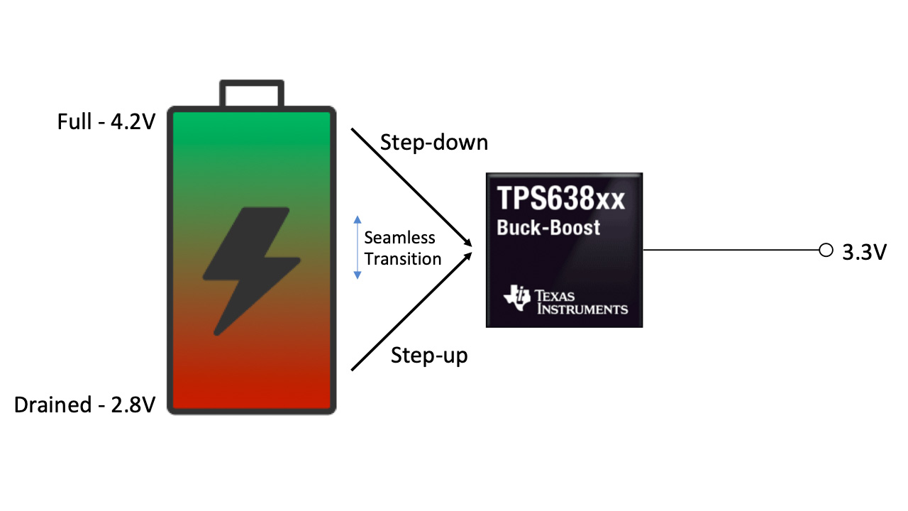
As an example, let’s assume that you needed to get 3.3 V out of a lithium-ion battery with a typical voltage range of 4.2 V to 2.8 V. If you used a buck converter, the battery cut-off voltage would need to be greater than 3.3 V, with the drawback of leaving energy stored in the battery unused. However, a buck-boost converter can help squeeze all of the energy out of the battery because it can also drain the energy stored when the input voltage is equal to or lower than 3.3 V, as visualized in Figure 2.

Figure 2: A buck-boost converter drains the battery completely


Using buck-boost converters as voltage stabilizers

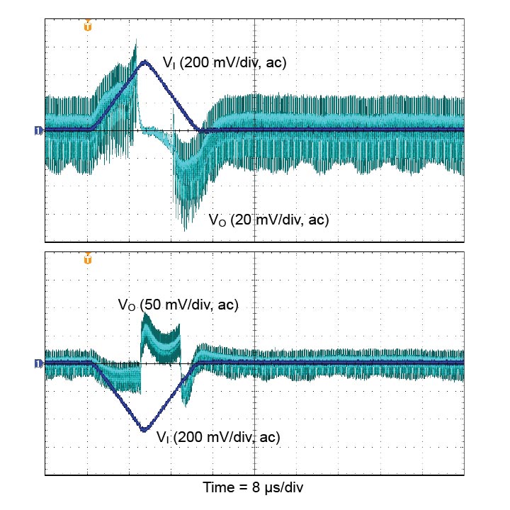
A second common use for a buck-boost converter is as a voltage stabilizer. You’ll need a voltage-stabilizing buck-boost converter if a supply rail has variations (such as 3.3 V with ±10% variation) while the load requires a more precisely regulated voltage (such as 3.3 V with ±5% tolerance). A more tightly regulated voltage could be required if components are sensitive to the supply voltage (such as transimpedance amplifiers in optical modules); if other DC/DC pre-regulators are not regulating tightly enough in industrial applications; or if other components such as e-fuses, load switches or long cables in the power path add voltage variation as a function of the current. A boost or buck converter alone could not solve this problem – a buck-boost converter, however, would be able to regulate the varying input voltage to the required, tighter limits. Figure 3 shows the TPS63802 responding to a fast ±0.5 V/10 µs line transient with significantly less than ±0.1V output voltage under-/overshoot.

Figure 3: Line Transient Response for the TPS63802 at VI = VO = 3.3V, ΔVI = ±0.5V

Additional applications for buck-boost converters

There are additional reasons to choose a buck-boost converter over a buck or boost converter alone. One of those reasons includes power ORing. Imagine a device such as a baby monitor powered by a 5-V USB wall adapter or two AA primary cells ranging from 3 V (when new) down to 1.6 V (when the batteries are drained). Only a buck-boost converter can accept a wide input voltage range from 5 V (wall adapter) down to 1.6 V (depleted battery while the wall adapter is not connected) and still generate a 3.3-V rail for the system. Apart from the buck-boost converter, you would only need two external diodes to avoid cross-currents from the wall adapter to the battery and to switch seamlessly to the battery if the wall adapter gets unplugged.

Buck-boost converter limitations

When the input voltage is close to the output voltage, the internal control loops of the buck-boost converter are often designed to toggle constantly between buck and boost mode. This works acceptably, but has drawbacks: mode toggling might show a varying switching frequency, a higher output voltage ripple and more electromagnetic interference (EMI). As a secondary effect, efficiency could dip slightly at this point.

To avoid the effects of mode toggling, look for devices with a dedicated buck-boost mode that keeps the output voltage ripple low. One example is TI’s new TPS638xx family of buck-boost converters, where a dedicated buck-boost mode and hysteresis avoid toggling with an easy-to-filter noise spectrum and lower EMI.

Can a buck-boost device handle all types of voltage conversion?

Since a buck-boost converter “contains” a buck and a boost converter, you could use it for any DC/DC voltage conversion – so from that perspective, the answer is yes. But there are more details to consider. Table 1 provides an overview of given input voltage ranges vs. the required output voltage, and if a buck-, boost- or buck-boost converter is a good solution.


 Input/output voltage

 Boost converter

 Buck converter

 Buck-boost converter

 VIN always higher than VOUT

 Does not work

 Ideal topology

 Works, but possible drawbacks in efficiency (one additional integrated transistor with on-resistance present in the conducting path), solution size (more silicon area needed) and quiescent current consumption

 VIN always lower than VOUT

 Ideal topology, but needs a specific setup for disconnecting the battery from the load when disabled

 Does not work

 VIN higher or lower than VOUT

 Does not work

 Does not work

 Ideal topology

 Boost and buck converter in series: works, but drawbacks in efficiency,   solution size, passive component size and costs

Table 1: DC/DC conversion topology overview

Let’s return to the original question serving as the title of this article: Is there a universal tool for DC/DC voltage conversion? Not exactly. Analog designers working on high-volume products will prefer the performance optimization of a dedicated boost or buck converter when a buck-boost converter is not required. However, designers working on small-volume products may consider that some trade-offs are worth the convenience.

Using a buck-boost universally (to buck-boost, boost and buck) could provide these benefits:

  • Scaling across projects, to save time and mitigate design risks.
  • Reducing the number of different DC/DC converters to a narrow list of easy-to-use buck-boost converters.
  • Streamlining procurement, with a less complex inventory, larger volumes for price leveraging and supply stability.
  • Benefitting from the fact that a buck-boost disconnects the load from the supply during shutdown, while other topologies might need an additional load switch.

Additional resources


When to use rechargeable batteries in small battery applications

$
0
0

From starting a car to powering a television remote, batteries provide the power that makes everyday objects possible. Yet not all batteries are made equal. Some are rated for lower temperatures, while others can provide higher peak-current discharge rates. Choosing the right battery can reduce an end product’s size, prolong its useful life and make it more robust.

When developing a new blood glucose monitor battery specification, your most critical decision will be whether the battery chemistry is disposable or rechargeable. Primary cells are typically cheaper, more energy dense and simpler to use – but also bulkier, wasteful and prone to leakage. As seen in Figure 1 below, rechargeable cells are more customizable in their performance, have longer lifetimes, and enable a sleeker and more compact design.

Figure 1: Typical rechargeable battery

Rechargeable batteries are also typically more expensive and complex to implement because of the additional components required for their operation. To many designers, these drawbacks mean that primary cells are the only choice for applications like blood glucose monitors. But rechargeable solutions add more value than just environmental benefits, even for simple and inexpensive devices.

To start, since it’s not possible to recharge primary-cell batteries, any device like a handheld monitor that uses them as a power source must factor in how much power is drained per hour of usage in order to determine the capacity needed for useful device run times. Consumers don’t like replacing the batteries on their devices daily or even weekly, so the capacity requirement must be many times the daily consumption.

To illustrate this fact, imagine that you’re designing a patch for monitoring posture at work. The device uses 50 mAh every eight hours at 4.2 V and has an intended 100 hours of use before replacement. To meet these performance targets with a primary cell, the capacity of the battery would have to be at least 625 mAh to provide enough power to the device. This unused capacity adds weight and size to a design that you could use elsewhere.

Meanwhile, a rechargeable battery would not need to last 100 hours; it only needs to power the worst case of use between charge cycles. If the device had 20 hours of use between rest periods, then you could design your system with a 125-mAh battery instead of the 625-mAh battery. Even though a primary-cell battery is three times as dense as its rechargeable alternative, this reduced capacity requirement more than compensates for the shortfall.

Another factor to consider with a primary-cell battery is battery content leakage, especially for alkaline-style batteries. As a battery is used, a chemical reaction occurs that can lead to an excess buildup of pressure within the cell. To cut costs, some primary-cell batteries are not made with the best venting or materials available. This leads to a structurally weak cell that over time can leak its contents onto sensitive electrodes, possibly damaging the affected device permanently. As a designer, why add another vector in which your device might fail?

Outside of the potential harm to the device, a primary-cell battery must be replaced semi-regularly. We have all had to change the battery in a remote after weeks of less-than-stellar signal strength. Once depleted, some primary cells require special disposal practices; all generate waste at higher rates than their rechargeable counterparts. As the world becomes more and more eco-conscious, you would be right to be concerned about the waste generated by millions of people replacing a battery every 100 hours vs. 2,000 hours of use, all because of your design choice.

Primary cells are at a steep disadvantage when dealing with growing energy consumption. Consumers like to be able to track their activity and other data through online applications. As things like Bluetooth® Low Energy and other communication standards are integrated into our everyday lives, energy demands increase and size decreases. Devices no longer sit idle when not in use but instead provide regular reports. This functionality expends energy, increasing the average energy per hour of use. Consumers will always want their devices to do more; rechargeable batteries enable that desire.

Chargers like the BQ25155 and the BQ25125 are small, simple to implement and powerful. With integrated low-dropout regulators, analog-to-digital and DC/DC converters, it is possible for these devices to be comprehensive battery-management units.

TI has a broad breadth of resources to guide you through the process of integrating a power-management system into your future designs, whether you’re an absolute novice or a power expert. From designs using 60-mAh batteries in your blood glucose monitors to the 5-Ah battery in your favorite power tool, we have a solution and support for any scenario.

Additional resources

Designing a headlight ECU with a high-power-density constant-on-time DC/DC buck LED driver

$
0
0

Advanced automotive headlights require dynamic lighting functionality to achieve road-safety-enhancing features like adaptive driving beam and adaptive front lighting systems. These features use LED matrix managers (LMMs) to perform dynamic brightness changes on individual LED pixels. The LED current of a headlight with normal brightness ranges from 350 mA to above 1 A. For such kind of current level, the board size built with traditional devices tend to be big. The trend of headlight is moving for more channels of dynamic lighting functions, there is a need to have a high-power-density DC/DC buck LED driver that supports dynamic load operations for further miniaturization of headlight driver systems.

Let’s review the electronic control unit (ECU) requirements for dynamic headlights implemented with LMMs. Because the LED stack or total string voltage changes dynamically with different road environments, it’s best if the current-providing LED drivers use the smallest possible capacitors. From [1], a boost-into-hysteretic buck architecture is the most optimal choice for ECUs. A buck converter provides a continuous output current to the LED in order to minimize the output capacitances, as shown in Figure 1.

Figure 1: Output current of a buck LED driver

A hysteretic control method best supports the dynamic brightness changes of LEDs, as shown in Figure 2.

Figure 2: Hysteretic operation of a DC/DC LED driver

The nature of hysteretic operation is that the switching frequency will change according to the ratio of the output voltage and input voltage, as shown in Figures 3 and 4, respectively.

Figure 3: Switching frequency vs. output voltage with a fixed input voltage (hysteretic operation)

Figure 4: Switching frequency vs. input voltage with a fixed output voltage (hysteretic operation)

Constant on-time control vs. hysteretic control – pseudo-fixed-frequency operation

For a hysteretic-controlled buck LED driver, the switching frequency changes according to the relationship between the input voltage and the output voltage. A changing switching frequency is sometimes not desirable, especially when trying to minimize electromagnetic interference (EMI). Most designs require a fixed switching frequency so that passive components can tackle the EMI generated around that switching frequency.

Constant on-time control is a hysteretic-based control scheme that provides pseudo-fixed-frequency operation. The duty cycle of the switching frequency is the ratio of the output voltage to the input voltage. If you can control the on time of the switching metal-oxide semiconductor field-effect transistor (MOSFET) such that it is proportional to the ratio of the output voltage to input voltage, then in theory, the switching frequency of the LED driver would stay the same.

Figures 5 and 6 are conceptual block diagrams of a constant on-time-controlled LED driver and the inductor current waveform.

Figure 5: Conceptual block diagram of a constant on-time-controlled buck LED driver

Figure 6: Inductor current ripple at different VIN-VOUT ratios

Since the on time is controlled according to the VIN and VOUT ratio, the duty cycle changes with a defined valley current limit. Therefore, the switching frequency is kept nearly constant, as shown in Figure 6.

Modern ECU requirements

A typical headlight ECU has an average of six to eight channels of output for different light uses: high beam, low beam, daytime running lights, position lights, turn indicators, fog lamps and so on. Figure 7 is a typical block diagram of an ECU. The total output power for such an ECU ranges from 60 W to 120 W. These specifications necessitate a small-sized yet efficient ECU solution – one that can fit in a tight spot within the car body without generating too much heat.

Figure 7: Typical ECU block diagram

The power-density advantage of the TPS92520-Q1

The TPS92520-Q1 monolithic synchronous dual-channel constant on-time DC/DC buck LED driver helps reduce ECU solution size and provides high power-conversion efficiency. It has a programmable switching frequency with up to 2.2-MHz operation. It accepts Serial Peripheral Interface commands from a microcontroller, thus minimizing the number of passive components around the device for parametric setup.

Integrating all four N-channel MOSFETs in the device not only saves space, but also improves power-conversion efficiency because MOSFETs provide a lower turn-on drain-to-source resistance (RDSON). More importantly, the device operates at above 1.8 MHz and reduces the physical size of the inductors. With two buck channels in one package, the number of devices to implement the ECU is half the number of channels; for example, three devices for six channels and four devices for eight channels.

In conclusion, a modern headlight ECU which supports dynamic lighting function requires buck LED drivers. With more and more channels having dynamic lighting functions, high-power-density LED drivers are required. High-power-density LED drivers (such as TPS92520-Q1) help implementing small-size, high performance headlight ECUs.

Additional resources

  1. Read this whitepaper on An ECU Architecture for Adaptive Headlights
  2. Check out the 120 W Dual-Stage Matrix-Compatible Automotive Headlight Reference Design
  3. TPS92520-Q1 buck converter for automotive headlamp ECU evaluation module

New LED drivers enhance your automotive lighting solutions

$
0
0

Automotive rear lighting systems have evolved from a signal that simply indicates a braking automobile to a symbol of an automotive brand.

Automotive rear lighting systems need to accommodate custom designs from automakers while still remaining useful for signaling. In this article, I’ll look further into automotive rear lighting system trends, new challenges that these trends bring and solutions that address these challenges.

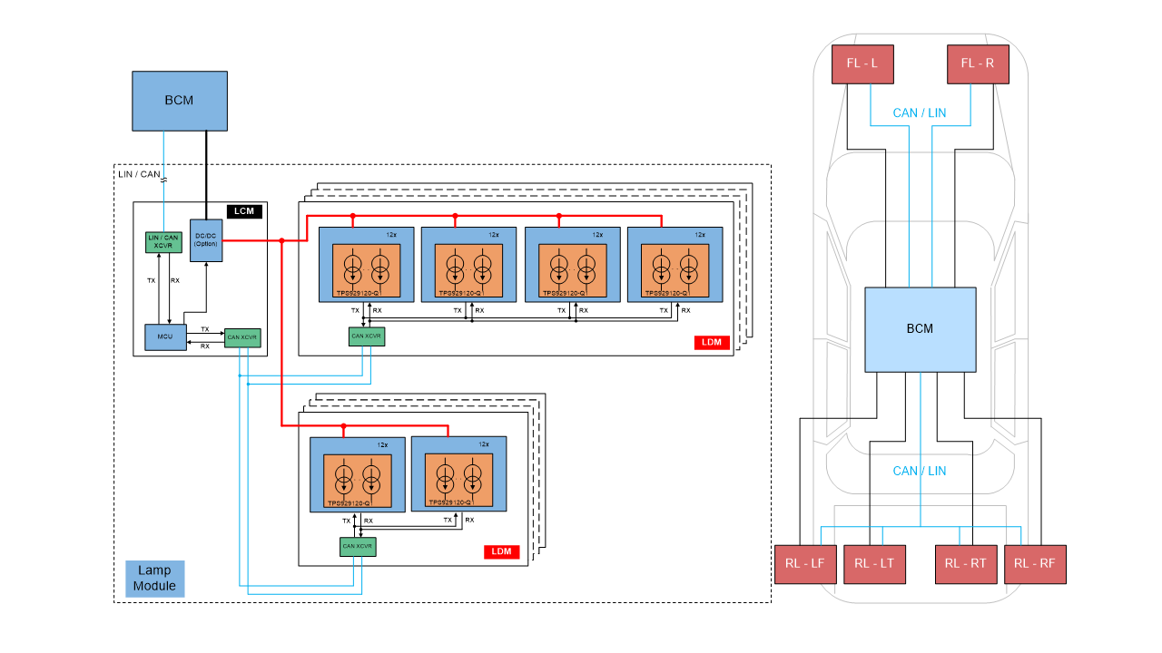
The first trend is unique animation in automotive rear lamps to symbolize a brand identity. Increased demand for complex animation in automotive lighting requires independent control of LEDs, but the first design challenge is that you cannot use enough analog LED drivers to drive the number of LEDs required to independently control a lighting application. Only LED drivers with a digital interface can effectively drive pixel-controlled lighting applications. Figure 1 shows the architectures for pixel control of a traditional rear lamp and a new rear lamp.

Figure 1: Traditional and new rear lamp architectures for pixel control

The second market trend of automotive rear lighting systems is that the shape of an automotive rear lamp is getting longer – sometimes, as shown in Figure 2, the rear lamp extends across the entire rear end of the car body.

Figure 2: Long automotive rear lamp

Automotive rear lamps that extend across the back of an automobile mean long wires across the entire printed circuit board. This presents a significant design issue, because the LED drivers must connect directly to a microcontroller (MCU), with wires in traditional single-ended interfaces for long-distance off-board communication. It is difficult for such a complex architecture to meet strict electromagnetic compatibility (EMC) requirements. Therefore, using an external physical layer transceiver is essential to effectively implement long distance off-board communication for automotive lighting, as shown in Figure 3.

 Figure 3: Typical application diagram for long-distance off-board communication

A third market trend is increasing the importance of robustness. The robustness of automotive rear lamps is directly connected to road safety, so drivers need to check the rear lamps of their automobiles regularly. Even a tiny mistake can lead to an accident. That’s why it’s essential to have automotive rear lighting systems capable of conducting self-diagnostics.

TI’s TPS929120-Q1 helps designers resolve the design challenges arising from automotive market trends. The TPS929120-Q1 is an automotive 12-channel LED driver with FlexWire interface that address the increasing need to individually control each LED.

By using an industry-standard CAN physical layer, the Universal Asychronous Receiver Transmitter-based FlexWire interface of the TPS929120-Q1 easily accomplishes long-distance off-board communication without impacting EMC.

Furthermore, the TPS929120-Q1 meets multiple regulation requirements with open-circuit, short-to-ground and single LED short-circuit diagnostics. A configurable watchdog automatically sets fail-safe states when the MCU connection is lost, and with programmable electrically eraseable programmable read-only memory, you can set the TPS929120-Q1 for different application scenarios.

The TPS929120-Q1 enables unique automotive lighting designs with improved performance as well.

Additional resource:

Selecting the right power MOSFET/power block package for your application

$
0
0

When starting a new design, engineers are often overwhelmed by the number of package options for power metal-oxide semiconductor field-effect transistors (MOSFETs) and power blocks. For example, TI offers single N-channel MOSFETs in 12 unique packages. Given this myriad of options, how do you know which package to select for your application?

There are many considerations when choosing a component package, including through-hole vs. surface mount, size, cost, lead spacing and thermal capability. In this technical article, I’d like to focus on package thermal capability and provide some rules of thumb for power dissipation in TI MOSFET and power block packages. I hope that you’ll find these rules helpful, because power dissipation determines the smallest package possible in a given application.

Start by looking at the data sheet

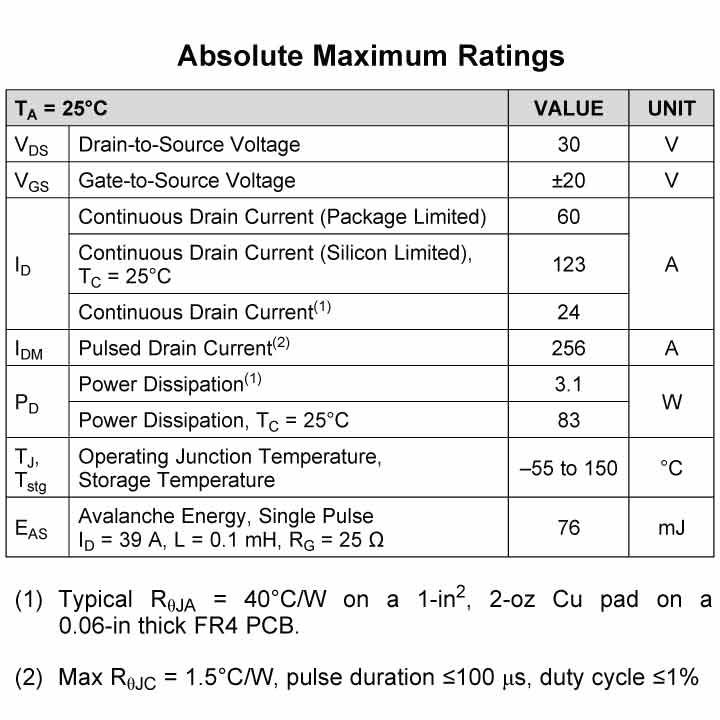
All power MOSFET and power block data sheets include thermal impedance specifications in the thermal information table. Figure 1 shows an example of thermal impedance specifications for the CSD17581Q5A.

Figure 1: Device absolute maximum ratings for the CSD17581Q5A

As detailed in an earlier technical article, the thermal impedance in the data sheet is determined using standard test procedures and printed circuit board (PCB) layout. Figure 2 depicts the standard test boards used to measure the thermal impedance of a 5-mm-by-6-mm small outline no-lead (SON) package. TI has developed similar standardized test boards for other TI MOSFET packages.

Usually, real-world applications use a PCB with two or more layers, thermal vias and a pad area somewhere in between those shown in Figure 2. These efforts result in low thermal impedance, allowing the heat to spread into the internal PCB layers for a space-optimized solution using the smallest board area.

Figure 2: 5-mm-by-6-mm SON junction-to-ambient thermal resistance (RθJA) measurements as they appear in the CSD17581Q5A data sheet 

The maximum power dissipation is specified in the absolute maximum ratings table (Table 1) of a power MOSFET/power block data sheet. Maximum power dissipation is a calculated value, as shown in this technical article, and in reality, it is not very useful because the standard PCB used for this type of testing does not correlate to actual, real-world applications. Start with the absolute maximum ratings but keep in mind that the thermal capability of a particular package may be better or worse in your application, with your PCB design and ambient conditions.

TA = 25°C (unless otherwise stated)

THERMAL METRIC

MIN TYP MAX

       UNIT

RθJC Junction-to-case thermal resistance(1)

1.5

        °C

RθJA Junction-to-ambient thermal resistance(1)(2)

50

(1) RθJC is determined with the device mounted on a 1-in2 (6.45-cm2), 2-oz (0.071-mm) thick Cu pad on a 1.5-in × 1.5-in (3.81-cm × 3.81-cm), 0.06-in (1.52-mm) thick FR4 PCB. RθJC is specified by design, whereas RθJA is determined by the user’s board design.

(2) Device mounted on FR4 material with 1-in2 (6.45-cm2), 2-oz (0.071-mm) thick Cu.

Table 1: CSD17581Q5A thermal impedance specifications

Consider design experience and empirical data

Fortunately, there are existing designs using MOSFET packages that can give you an idea of the thermal capabilities of each package in real-world conditions. Combined with empirical data collected during testing, you should have some guidance for the amount of power that can be dissipated in a particular power MOSFET package. Tables 1 through 5 summarize the estimated maximum power dissipation by product category and package type.

Keep in mind that the power dissipation numbers in the tables below are only estimates. Because the effective junction-to-ambient thermal impedance is very dependent upon the PCB design, your actual performance may vary; in other words, your particular design may be able to dissipate more or less power than what is presented here. Use these guidelines to help narrow down what packages to consider for your design.

How to read the tables

Let’s consider the 5-mm-by-6-mm plastic SON package. TI uses a few versions of this SON package for its power MOSFETs and power blocks. Most vendors have a similar package for their power devices, and a lot of data exists about how much power it can dissipate. TI has tested power blocks in this package on a PCB design with dimensions of 4 inches wide by 3.5 inches long by 0.062 inches high and six copper layers of 1-oz copper thickness. Based on the test results, a good rule of thumb is that the 5-mm-by-6mm SON package can dissipate about 3 watts in a typical application with a good layout.

Product category = single N-channel MOSFET

Package description

Package type (drawing)

Dimensions (mm)

Typical RθJA (°C/W)

Estimated PDISS (W)

FemtoFET™

PicoStar™ package (YJM)

0.73 by 0.64

255

0.5

FemtoFET™

PicoStar package (YJC, YJJ)

1.0 by 0.6

245

0.5

FemtoFET™

PicoStar package (YJK)

1.53 by 0.77

245

0.5

Wafer-level package (W, W10)

DSBGA (YZB)

1.0 by 1.0

275

0.4

Wafer-level package (W1015)

DSBGA (YZC)

1.0 by 1.5

230

0.5

2-mm-by-2-mm SON (Q2)

WSON (DQK)

2.0 by 2.0

55

2.2

Wirebond 3-mm-by-3mm SON (Q3A)

VSONP (DNH)

3.3 by 3.3

48

2.5

Clip 3-mm-by-3mm SON (Q3)

VSON-CLIP (DQG)

3.3 by 3.3

48

2.5

Wirebond 5-mm-by-6-mm SON (Q5A)

VSONP (DQJ)

5.0 by 6.0

40

3.0

Clip 5-mm-by-6-mm SON (Q5B)

VSON-CLIP (DNK)

5.0 by 6.0

40

3.0

Clip 5-mm-by-6-mm SON (Q5)

VSON-CLIP (DQH)

5.0 by 6.0

40

3.0

TO-220 (KCS)

TO-220

N/A

24

5.0

D2PAK (KTT)

DDPAK/TO-263

N/A

30

4.0

Table 2: Single N-channel MOSFET estimated power dissipation by package


Product category = dual N-channel MOSFET

Package description

Package type (drawing)

Dimensions (mm)

Typical RθJA (°C/W)

Estimated PDISS (W)

LGA (L)

PicoStar package (YME)

1.35 by 1.35

175

0.7

LGA (L)

PicoStar package (YJE)

2.2 by 1.15

150

0.8

LGA (L)

PicoStar package (YJG)

3.37 by 1.47

92.5

1.3

Wafer-level package (W1723)

DSBGA (YZG)

1.7 by 2.3

140

0.9

2-mm-by-2-mm SON (Q2)

WSON (DQK)

2.0 by 2.0

55

2.2

3-mm-by-3-mm SON (Q3E)

VSON (DPA)

3.3 by 3.3

50

2.4

S0-8 (ND)

SOIC (D)

5.0 by 6.0

60

2.0

Table 3: Dual N-channel MOSFET estimated power dissipation by package

Product category = single P-channel MOSFET

Package description

Package type (drawing)

Dimensions (mm)

Typical RθJA (°C/W)

Estimated PDISS (W)

FemtoFET™

PicoStar package (YJM, YJN)

0.73 by 0.64

255

0.5

FemtoFET™

PicoStar package (YJC, YJJ)

1.0 by 0.6

245

0.5

FemtoFET™

PicoStar package (YJK)

1.53 by 0.77

245

0.5

LGA (L)

PicoStar package (YMG)

1.2 by 1.2

225

0.5

Wafer-level package (W10)

DSBGA (YZB)

1.0 by 1.0

275

0.4

Wafer-level package (W, W1015)

DSBGA (YZC)

1.0 by 1.5

230

0.5

Wafer-level package (W, W15)

DSBGA (YZF)

1.5 by 1.5

220

0.5

2-mm-by-2-mm SON (Q2)

WSON (DQK)

2.0 by 2.0

55

2.2

Wirebond 3-mm-by-3-mm SON (Q3A)

VSONP (DNH)

3.3 by 3.3

48

2.5

Clip 3-mm-by-3-mm SON (Q3)

VSON-CLIP (DQG)

3.3 by 3.3

48

2.5

Table 4: Single P-channel MOSFET estimated power dissipation by package


Product category = dual P-channel MOSFET

Package description

Package type (drawing)

Dimensions (mm)

Typical RθJA (°C/W)

Estimated PDISS (W)

Wafer-level package (W1015)

DSBGA (YZC)

1.0 by 1.5

230

0.5

Wafer-level package (W15)

DSBGA (YZF)

1.5 by 1.5

220

0.5

Table 5: Dual P-channel MOSFET estimated power dissipation by package

Product category = N-channel power block

Package description

Package type (drawing)

Dimensions (mm)

Typical
RθJA (°C/W)

Estimated PDISS (W)

LGA (P)

PTAB (MPC)

3.0 by 2.5

67

1.8

LGA (N)

PTAB (MPA)

2.5 by 5.0

56

2.1

LGA (M)

PTAB (MPB)

5.0 by 3.5

50

2.4

Clip 3-mm-by-3mm SON (Q3D)

LSON-CLIP (DQZ)

3.3 by 3.3

58

2.1

Clip 5-mm-by-6-mm SON (Q5D)

LSON-CLIP (DQY)

5.0 by 6.0

40

3.0

DualCool™ 5-mm-by-6-mm SON (Q5DC) packaging

VSON-CLIP (DMM)

5.0 by 6.0

40

3.0


Table 6: N-channel power block estimated power dissipation by package

Conclusion

You can use the information presented in this technical article to guide your package selection for power MOSFETs and power blocks. Always check that the MOSFET power loss in your application does not exceed the package capability. These are not absolute limits and the performance in your application will depend on the operating and environmental conditions, as well as the PCB layout and stackup.

Of course, power dissipation is not the only consideration when selecting a power device for a design. You’ll also have to consider other parameters such as voltage and current ratings, on-resistance, package size, and lead spacing.

Additional resources


Address thermal performance in small applications with the power WCSP technology

$
0
0

When it comes to cost-effectively powering space-constrained, high-power-density applications, such as solid-state drive (SSD) or wearable equipment, wafer chip-scale package (WCSP) DC/DC converter solutions are widely used in the industry. The trend toward even tighter integration into system-in-package (SIP) modules poses an increasing challenge to established packaging techniques, forcing engineers to look for new ways of optimizing thermal performance in space-constrained applications.

Thermal performance and solution size, particularly maximum profile height, are very real challenges that every SIP designer experiences. As the designer of a low-form-factor SIP module for your next application, you may be searching for a power device that will fit in the tiny space you have and that will also stay cool while delivering the power you need for your system.

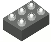
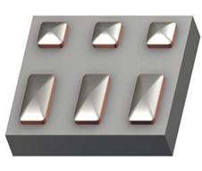
TI’s power chip-scale packaging (power WCSP) is a low-profile WCSP enhancement that focuses on thermal performance and current density optimization. Unlike a standard WCSP, which uses a fixed ball diameter (Figure 1a), power WCSP takes advantage of the flexibility of copper post sizes to increase the area of key interconnects like power pins, without having to increase the die size or infringe upon the spacing tolerance of surface-mount manufacturing technologies. The copper posts can be square or rectangular, with a total stack thickness as small as 85 µm (Figure 1b). The shape of the posts makes it possible to achieve a significant surface gain for critical pins, thereby increasing current-handling capacity as well as improving the heat transfer and thermal performance of the package. At the same time, the package height can be as low as 0.3 mm, enabling easy implementation into high-power-density and space-critical integrated solutions.

Figure 1: 6-pin standard WCSP package (a); 6-pin power WCSP package (b)

TI’s TPS62088 DC/DC converter demonstrates the thermal performance of power WCSP packaging. The TPS62088 is a 1.2-mm-by-0.8-mm, high-efficiency 2.4-V to 5.5-V input, 3-A DC/DC buck converter operating at a 4-MHz switching frequency. The device is available in two package options: either the standard WCSP (TPS62088YFP) or the new power WCSP (TPS62088YWC). Looking at the thermal properties of these otherwise identical devices in each package option allows us to make a clear comparison of the thermal performance of the two packaging technologies.

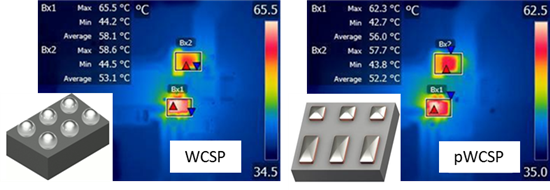
Figure 2a shows the thermal performance of the TPS62088YFP (WCSP) and Figure 2b shows the TPS62088YWC (power WCSP) operating at VIN = 5 V, VOUT = 1.8 V and IOUT = 3 A, taken at room temperature with an infrared camera. Due to very low junction-to-top characterization parameter values – ΨJT = 0.5-0.7°C/W for both packages – you can assume that the junction temperature is roughly equal to the case temperature. The results indicate that the temperature of the power WCSP device is reduced by as much as 3°C compared to the standard WCSP device, considering the device and printed circuit board (PCB) layout solution together.

The TPS62088YWC power WCSP version, while increasing power density by reducing profile height from 0.5 mm to 0.3 mm, enables you to optimize the thermal performance of your system by improving the heat transfer to the PCB through the larger bump structures. Of course, designing your application for optimal thermal performance implies paying attention to further aspects of the system as well. Proper PCB layout results in smaller junction-to-ambient and junction-to-board thermal resistance, thereby reducing the device junction temperature for a given dissipated power and board temperature. Wide power traces can also efficiently sink dissipated heat. Keep in mind that many system-dependent properties such as thermal coupling, airflow, added heat sinks and convection surfaces, and the presence of other heat-generating components, affect the power dissipation capabilities of a given device.


Figure 2: Thermal performance of the TPS62088 (measurement point: Bx1) operating at VIN = 5 V, VOUT = 1.8 V and IOUT = 3 A taken at room temperature: TPS62088YFP WCSP version (a); TPS62088YWC power WCSP version (b)

Many space-constrained applications like SIP modules, SSDs or wearable devices, require the total power solution, (not just the power IC), to fit in the thinnest spaces possible. The TPS62088YWC’s high switching frequency allows you to use tiny, low-form-factor 0.24-µH inductors to shrink the solution size to 15 mm2, and take full advantage of the 0.3-mm profile height for the whole power circuit.

Additional resources

Powering tiny industrial automation control equipment with high-voltage modules: how to ensure reliability

$
0
0

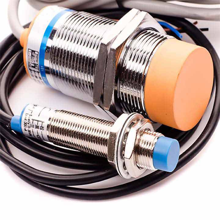
It’s not unusual to find industrial automation control equipment like field sensors (for proximity, pressure, flow or temperature, for example) housed in increasingly inconspicuous packages. Figure 1 shows an example of a proximity sensor housed in a tiny screw (which can be as small as 8 mm or in some instances even smaller). While the electronics that go into the housing have to be ultra-small, they still need to be rated for the right parameters to ensure long-term equipment reliability.

Figure 1: Typical proximity sensor

Addressing the challenges of unregulated input voltages

Electronics in smart sensors may include a low-power microprocessor, analog-to-digital signal-processing circuitry and a voltage regulator. Sometimes, designers might not consider power until the end of the design process; therefore, the space allotted to power can be really sparse.

A typical application for power-conversion circuitry in factory automation equipment might be down-converting a 24-V input voltage and regulating it to the required potential. The 24-V input voltage might be a standard industrial bus which could have an input voltage as low as 8 V or as high as 36 V.

Sensors in process automation need to withstand overvoltage transients. The severity of voltage transients depends on how the 24 V was derived. In some situations, where the lead lengths cover long distances in the field, the industrial 24-V bus may experience higher voltage transients. In addition, field applications could have clamp circuits that limit the voltage transient to a safe extra-low voltage limit. This means that in a short-circuit condition; the output of the industrial bus could be stuck at 60 VDC.

Considering another example, a 24 VAC could be an input source. The maximum root-mean-square voltage of such a supply can often swing to 28 V, leading to a peak voltage delivered that’s close to 40 V. The overvoltage protection setting on the input supply could be about 120% of the peak voltage, which takes an input voltage close to 48 V.

In these examples, it is important to use a voltage regulator rated for the maximum DC voltage at the input to ensure uninterrupted operation of equipment like field sensors.

Ensuring appropriate pin spacing for long-term reliability

The TPSM265R1 is a high-voltage embedded power module rated for 65 V that integrates the voltage regulator and inductor. This gives the device enough margins to cover potential overvoltage conditions. However, just because a power module has an integrated high-voltage regulator doesn’t mean that you can safely rate it for the high voltage. To properly rate the device for a higher input voltage requires appropriate design of the pad/pin spacing on the module. The Association Connecting Electronics Industries has a standard called IPC 2221-B which goes over this in detail.

The IPC-2221B standard lists the minimum spacing between the edges of conductors that is required to ensure proper operation at worst-case voltages. To ensure that the regulator can indeed sustain a peak voltage of 65 V the spacing between the edges of the conductors must be at least 0.5 mm.

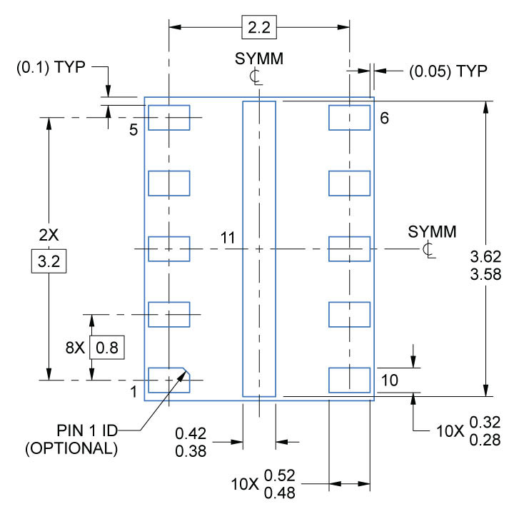
Figure 2 shows the pin pitch of the TPSM265R1, which is 0.8 mm; the width of the pad is typically 0.3 mm. From edge to edge, the space between the pads is 0.5 mm, in compliance with the IPC-2221B requirement.

Figure 2: TPSM265R1 package drawing

Meeting the requirement for a small solution size

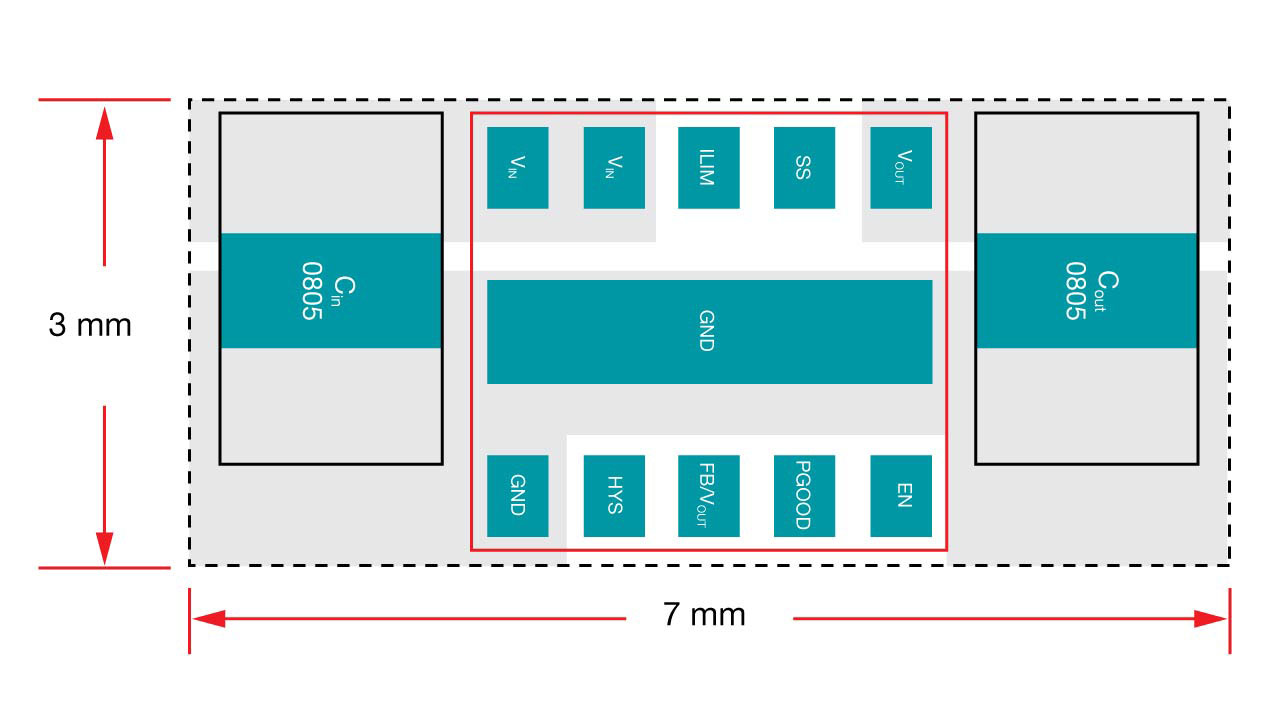
IPC spacing requirements put system designers at odds with the requirement for miniaturization. After all, I began this technical article talking about how electronics need to fit into an 8-mm screw. To address both spacing requirements and miniaturization requirements, designers have to be smart about designing the power module. TI designed the layout of the TPSM265R1 package with a small-solution space in mind. Figure 3 shows an example layout, with the minimum required components for a fixed-voltage option of 3.3 V or 5 V.

Figure 3: Example layout with the TPSM265R1

The module package size is 2.8 mm by 3.7 mm. To complete the circuit, you only need two capacitors. With two 0805 capacitors, the overall solution size for a 5 V or 3.3 V output can be as small as 3 mm by 7 mm. The placement of the input capacitor so close to the module’s VIN and GND pins makes for a “quiet” switching operation, with less ringing on the switch node.

When designing the power supply for small industrial automation control equipment, it’s important to choose products with appropriate ratings for a reliable operation. Well-designed power modules will not only help engineers address size challenges and ensure long-term reliability but can also help simplify the design process.

Additional resources

Get more out of your power supply with port power management

$
0
0

With the publication of the new Institute of Electrical and Electronics Engineers 802.3bt standard, the power range of Power over Ethernet (PoE) loads continues to expand. If you are designing systems that provide PoE, this presents a challenge. You may need to provide 5 W of power to a low-end Internet Protocol camera or 70 W to a high-end wireless access point (WAP). An enterprise switch with 48 ports that can simultaneously support 90 W on all ports would require a 4.3-kW supply.

You probably want to enable the full functionality of the high-end WAP, but do you really want to pay for the giant power supply? Knowing the typical use case of your system, you can choose a smaller power supply that would be sufficient in most situations. But, how do you prevent the supply from overloading in the rare event that all loads draw full power?

Port power management (PPM) algorithms can come to your rescue. When a new device is plugged in, the system will only turn the device on if there is enough remaining power. A system that supports priority and exceeds its power budget will actually shut down a lower-priority load when a higher-priority load is plugged in.

At a high level, PPM is a simple concept, but it can have multiple flavors, and its implementation can be tricky. Typically, there are multiple power sourcing equipment (PSE) devices, thus requiring a central microcontroller (MCU) to manage the system. Also, the system could have slots for multiple power supplies, which can get plugged in or unplugged during operation.

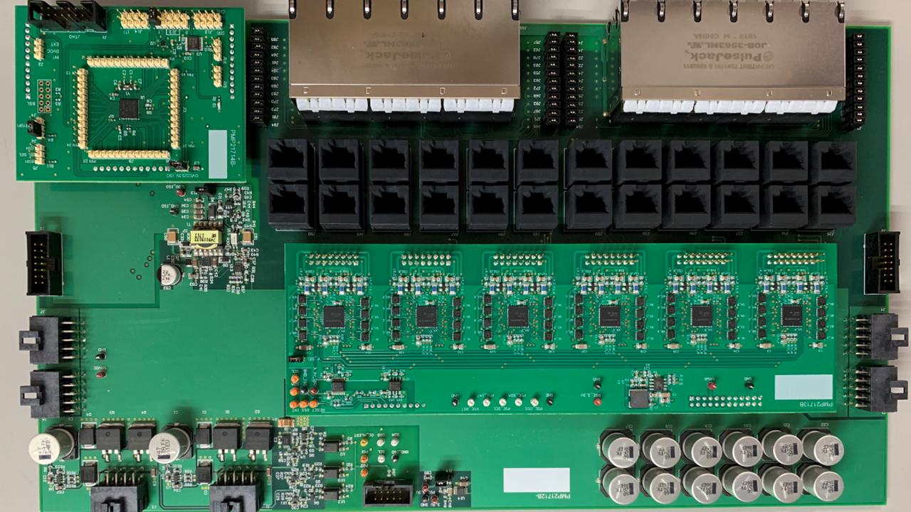
TI’s FirmPSE ecosystem can give you a huge head start in implementing PPM in your end equipment by removing the burden of writing low-level code to control the PSEs. Figure 1 shows the evaluation board of TI’s FirmPSE, which is implemented using an MSP430™ MCU and TPS23881 PSE. TI provides a binary image that you can load directly into the MSP430F5234. You will need to write code that interfaces between the host central processing unit (CPU) and the MSP430F5234 to configure the system and monitor the port status.

 Evaluation board of TI’s FirmPSE ecosystem

Figure 1: Evaluation board of TI’s FirmPSE ecosystem

TI’s ecosystem features:

  • Orderable TI designs with twenty-four 90-W PoE ports.
  • A user’s guide.
  • A binary image that can be loaded directly to the MCU.
  • A host interface document defining the interface between the MSP430F5234 and host CPU.
  • A graphical user interface to configure the binary image and to evaluate monitor port status’s of the FirmPSE system.


To learn more about PPM and ways to reduce your power supply consider watching our FirmPSE system firmware GUI offline mode or online mode training videos.


Sequencing and powering FPGAs in radar and other defense applications

$
0
0

Aerospace and defense applications, from ruggedized communications to radar to avionics equipment, require intelligent power with accurate voltage regulation, high power density, high efficiency and comprehensive system diagnostics for high reliability.


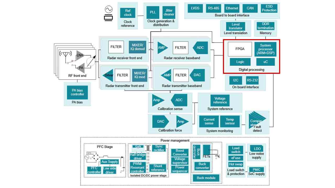
More and more aerospace and defense applications are using faster, higher-performance processors and field-programmable gate arrays (FPGAs). As shown in Figure 1, radar requires not just a DC/DC converter for the digital signal processor (DSP), FPGA and input/output (I/O) rails, but also a sequencer to provide accurate sequencing for power-up and power-down scenarios.

Figure 1: Radar block diagram

Why do you need to sequence the power rails?

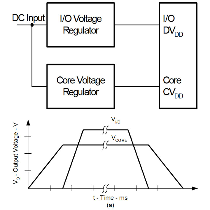
Improperly sequenced power rails present several risks to the power supply, including compromised reliability (which can lead to device failures), stress on the integrated circuit, reduced application life and immediate faults, which relate to excessive voltage differentials and current inflow. Figure 2 shows a typical power-sequencing diagram.

Figure 2: Power-sequencing diagram


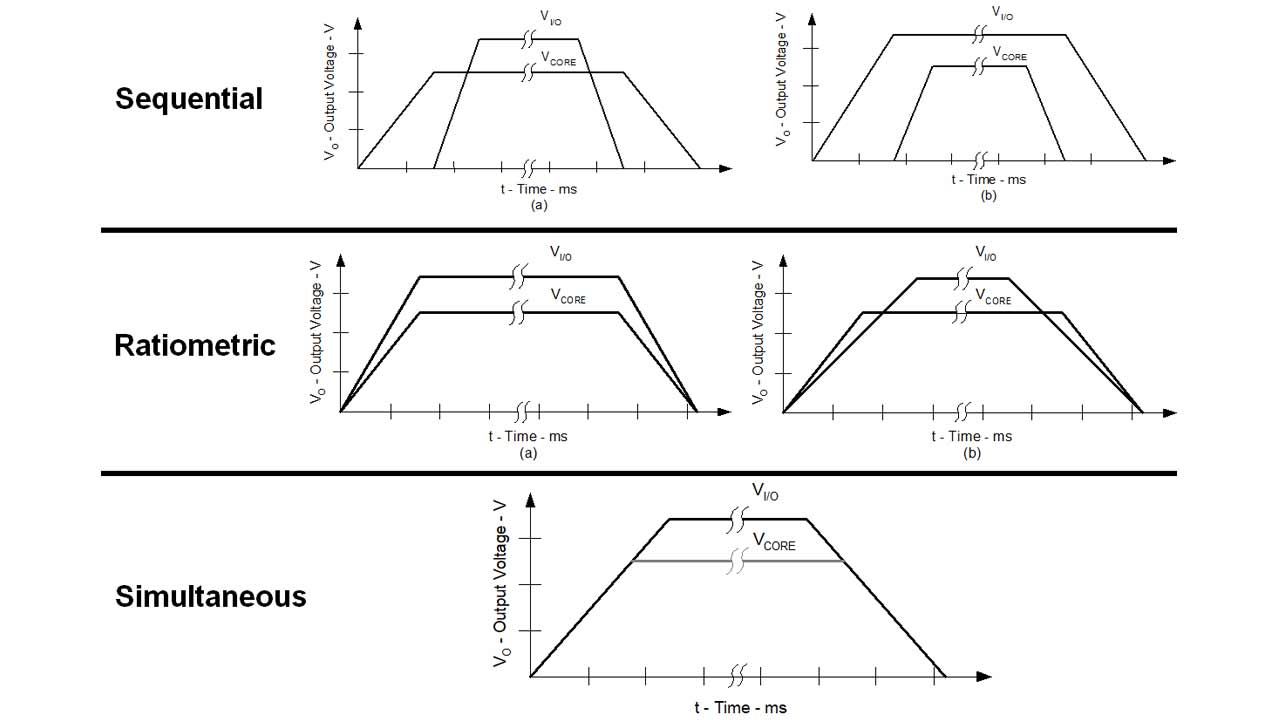
As shown in Figure 3, there are three types of sequencing schemes: sequential, ratiometric and simultaneous:

  • Sequential is when two or more voltage rails power up or power down in sequence at different slew rates and with different final values.

  • Ratiometric is when two or more voltage rails power up or power down at the same time at different slew rates and with different final values.

  • Simultaneous is when two or more voltage rails power up or power down at the same time with the same slew rate but different final values.


Figure 3: Types of voltage rail sequencing


The ability to address all of these sequencing schemes but also monitor the power-supply rails and report system warnings and faults with flexibility and ease of use is critical in order to prevent runaway issues like overcurrent and overtemperature.


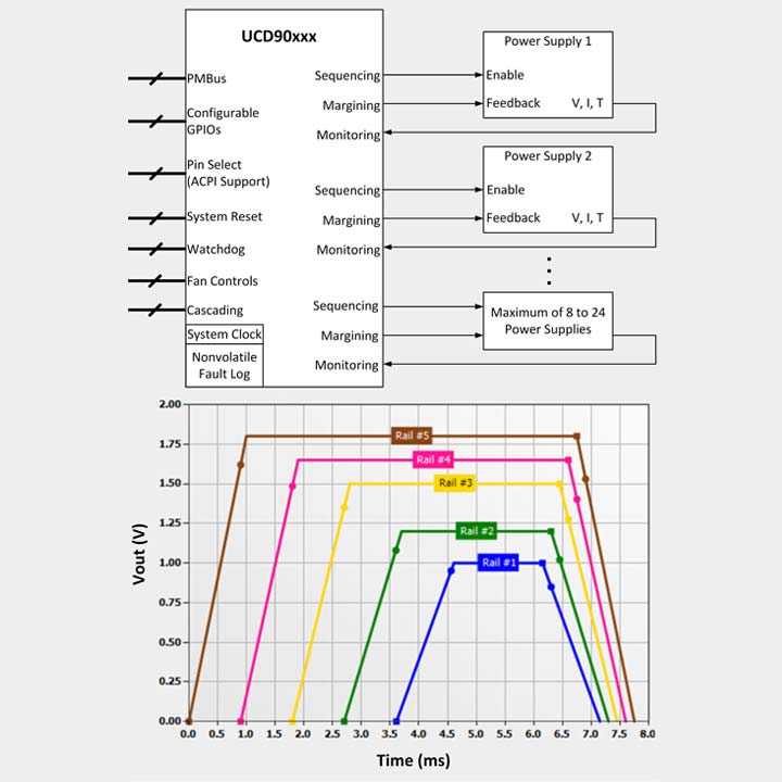
The UCD90320Uis TI’s newest 32-channel PMBus sequencer which can be programmed and reconfigured through its onboard nonvolatile memory for a wide range of sequencing scenarios through the Fusion Digital Power™ Designer graphical user interface, as shown in Figure 4.


Figure 4: Voltage rail sequence timing configuration window in Fusion Digital Power Designer


Dealing with ionizing radiation exposure


In radar and other defense applications, there may be instances of ionizing radiation exposure. When this happens, the failure-in-time (FIT) rate can increase; that is, the probability of failure can increase. A typical instance of ionizing radiation failures in semiconductors is a single-event upset (SEU). An SEU is caused by ionizing radiation strikes that discharge the charge in storage elements such as configuration memory cells, user memory and registers, resulting in a bit flip as shown in Figure 5. The change caused by an SEU is considered “soft” because the circuit/device itself is not permanently damaged by the radiation. If a new data is written to the bit, the device will store the new data correctly.


Figure 5: An ionizing radiation SEU affecting a memory cell


In terrestrial applications, the two radiation sources of concern are alpha particles emitted from package impurities and high-energy neutrons caused by the interaction of cosmic rays with the earth’s atmosphere. Studies conducted over the last 20 years have led to high-purity package materials (ultra-low alpha [ULA]), which can minimize SEU effects caused by alpha particle radiation. Unavoidable atmospheric neutrons remain the primary cause of SEU effects today.


The UCD90320U uses a compact 0.8-mm pitch ball-grid array package with a ULA mold compound to reduce the soft errors caused by ionizing alpha particles. This sequencer/monitor also has the ability to scan the user-configuration static random access memory to detect SEUs. Both ULA and SEU detection features provide higher reliability for radar and other defense applications. Based on actual customer results, the FIT rate dropped to 10 with the UCD90320U in the ULA package, versus a FIT rate of 1,344 with the non-ULA package.


Achieving effective voltage regulation


After successfully sequencing the FPGA rails, the FPGA core rail is the most critical in terms of voltage regulation, power density, thermal performance and efficiency. Some of the latest FPGAs require a total tolerance of ±2% DC plus AC (AC = load transient), which makes voltage regulator design challenging. Table 1 lists typical high-current FPGA core and I/O rail design specifications.


PARAMETER

SPECIFICATIONS

Input supply

12 V, ±5%

Switching frequency

500 kHz

Power stages

CSD95490Q5MC

Core rail

Nominal output voltage

0.9 V

DC+AC tolerance

±2%

Max output current

120 A

DC load line

-           

Max load step

30 A at 100 A/μs

Number of phases

3

COUT, BULK

12x 470 μF, 2.5 V, 3 mΩ

COUT, MLCC

22x 220 μF, 4 V, X5R

I/O rail

Nominal output voltage

0.9 V

DC+AC tolerance

±2%

Max output current

20 A

DC load line

-

Max load step

10 A at 100 A/μs

Number of phases

1

COUT, BULK

8x 470 μF, 2.5 V, 3 mΩ

COUT, MLCC

8x 220 μF, 4 V, X5R


Table  1: High-current FPGA core and I/O rail power specifications

Radar and other defense equipment customers typically prefer power modules for the ease of use and maintenance-free benefit. For an FPGA requiring 120 A of output current, an equivalent discrete multiphase buck voltage regulator solution requires 66 discrete components and hundreds of hours of design, layout, lab testing, prototyping, reliability and final testing. The design will also be subjected to electromagnetic compatibility testing, and for defense applications, shock and vibration testing as well.

For the highest-performance FPGA, TI’s TPSM831D31120-A plus 40-A dual-output PMBus buck module can help designers meet ±2% DC and AC tolerance specifications at high power densities, with 243 W of output power in 720 mm2 of printed circuit board area.


Employing our proprietary DCAP+™ control mode, the TPSM831D31 can reduce the output capacitor count, including the number of multilayer ceramic capacitors required to maintain output voltage regulation during severe load transients. The TPMS831D31 can power both the FPGA core and I/O rails, as shown in Figure 6.

Figure 6: TPSM831D31 application circuit

If you are designing a radar or any other defense equipment using high-current FPGAs and your design priorities are comprehensive sequencing, monitoring, ease of use and high power density for your FPGA DC/DC converter, consider using reconfigurable PMBus sequencers such as the UCD90320U and high-performance modules such as the TPSM831D31.


Additional resources:


3 tips when designing a power stage for servo and AC drives

$
0
0

The Industry 4.0 revolution enables the capture and analysis of data about various machines, resulting in faster, more flexible, more reliable and more efficient processes to produce higher-quality goods at lower costs. Industry 4.0 does create some challenges at the system level, however, for engineers designing power supplies with DC/DC step-down regulators. These challenges include the need to improve reliability, enhance heavy load efficiency to minimize thermal dissipation, and provide a faster transient response to achieve a smaller output capacitance.

1. Think about wide input voltage and high current.

Figure 1 shows a simplified power architecture for a servo drive power stage, which is powered by a 24-VDC auxiliary power source. The 24-V can also be generated by the DC Bus voltage by using an isolated power supply. The first stage is the field input protection circuit; the second stage is the nonisolated DC/DC field power supply.

Figure 1: Servo drive module power architecture

The power supply typically needs to support 36-V or even up to 60-V operation and requires DC/DC converters rated for higher current (>1 A) to protect against unexpected power surges caused by long cables, hot plugs and ringing – familiar scenarios for engineers designing power solutions for the industrial world. As such, when designing a power supply for industrial applications like servo or AC drives, consider step-down converters that offer a wide input voltage.

The LMR36520 has a transient tolerance as high as 70 V, which helps protect against overvoltages and meets the surge immunity requirements of International Electrotechnical Commission 61000-4-5. If 36 VIN is acceptable for your application, you can pick converters based on the required load conditions. The LMR33610, LMR33620, LMR33630 and LMR33640 enable you to reuse most of your layout, significantly simplifying your system-level schematic and layout design and reducing R&D efforts.

2. Choose devices with fast transient response.

Because of their ruggedness, AC drives can be used to control the induction motors used in processing plants. Besides that, AC drives control the speed of an AC motor by varying the output voltage and frequency through a sophisticated microcontroller (MCU)-controlled electronics device. Figure 2 shows the power-supply design for a safety MCU in AC drive system. This safety power supply (3.3 V) is designed to power up the safety MCU and other loads. The power supply can also be used for servo drives besides the AC drive.

Figure 2: Power-supply design for servo drive system

Higher supply voltage can affect the normal operation of an MCU or even damage it, when the supply voltage is higher than the MCU’s absolute maximum supply voltage rating. Lower supply voltage, in turn, can negatively impact MCU’s reset circuits’ or peripheral circuits’ (such as general purpose input/output -GPIO) drive capability, preventing them from operating normally. Thus, when using a power supply to power both an MCU and another dynamic load, consider devices that offer fast transient performance. During the load transient, those devices will have lower overshoot/undershoot voltage at the output side, without impacting the operation of the MCU. Fast transient performance reduces the pressure on the MCU and secondary point of load regulators, improving system robustness and potentially eliminating the need for protection devices such as clamping diodes.

Figure 3 shows the load transient and switching waveforms of the LMR36520. When the load increases from 1 A to 2 A at a 1-A/µs slew rate, there is only 100 mV of overshoot and undershoot.

Figure 3: LMR36520 load transient

3. Don’t forget about ground protection.

The power supply will also need output-short-to-ground protection. The power-supply output from Figure 2 also powers buffers and communication interfaces. In a real-life industrial environment, an operator might forget to turn off the power when changing some component, which could cause the power supply’s output (3.3 V or 5 V, depending on the MCU) to short to ground. When a 3.3-V or 5-V load is shorted to ground and released, you don’t want to see overshoot at the 3.3-V or 5-V rail because that might damage the MCU, which usually has an absolute maximum operation input voltage of 6 V. To prevent overshoot, look for buck converters with properly designed hiccup-protection features. As Figure 4 shows, the LMR36520 has good output-short-to-ground recovery protection.


Figure 4: LMR36520 short-to-ground waveform

Conclusion

When designing the power supply for a servo and AC drive, think through the potential impact of your design. A wide input voltage, higher output current, fast transient performance and good short-to-ground protection are the key factors you should consider during development.

Additional resources

How to flexibly configure an LED driver for automotive headlights

$
0
0

Electronic technology has advanced so that an electronic control unit (ECU) is required to control the functions of full LED automotive headlights. An ECU consists of mainly LED drivers for headlight functions such as high beams, low beams, daytime running lights, position lights, turn indicators and fog lights. In this article, I’ll explain the advantage of having a flexibly configurable LED driver.

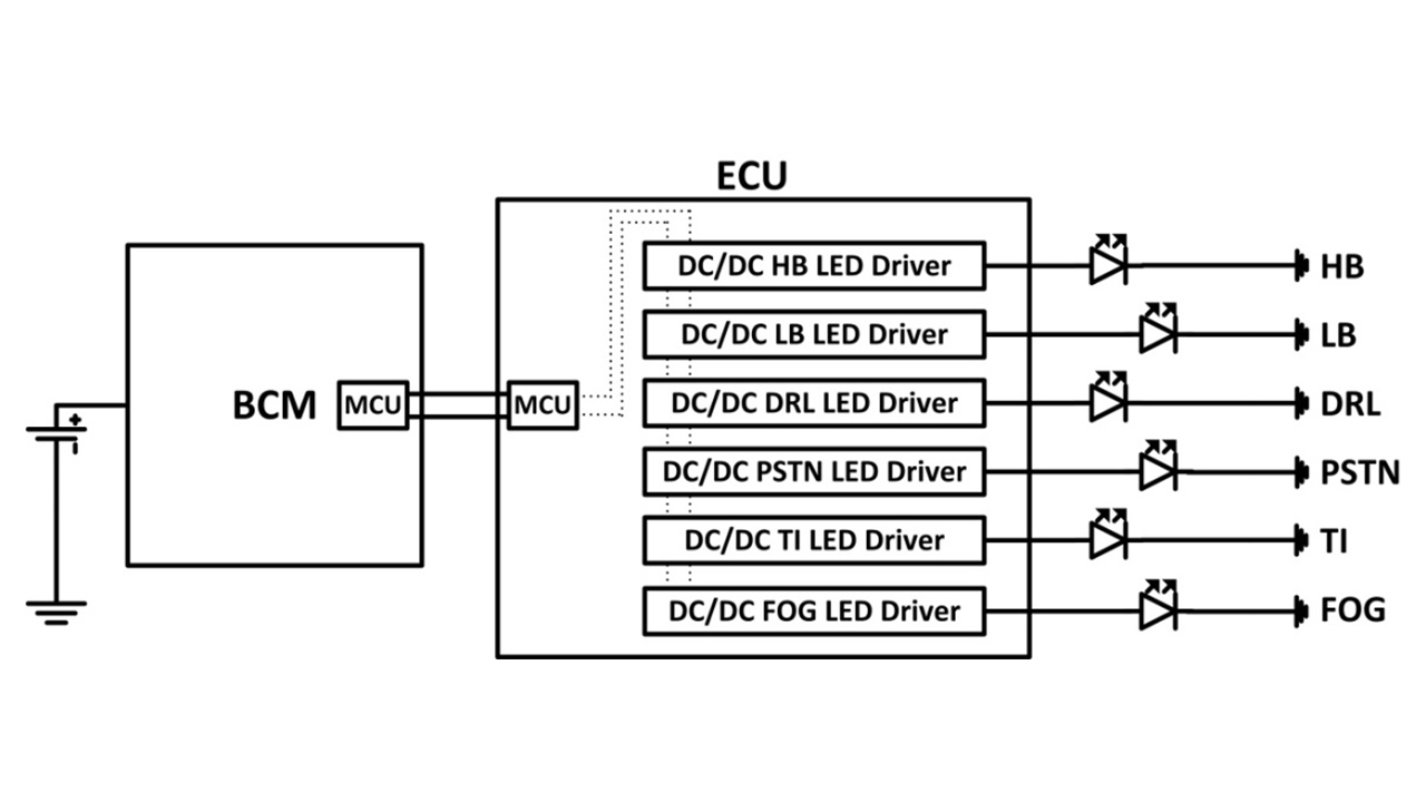
When LEDs were first introduced into the automotive headlight space, high-side switches connected to LED drivers drove the corresponding LEDs in each of the headlight functions. Figure 1 shows a block diagram of a traditional automotive body control module (BCM) with LED drivers for corresponding headlight functions. The LED and input voltage relationship per headlight function determine the best DC/DC topology.

Figure 1: Traditional automotive BCM with DC/DC LED drivers for LED headlights

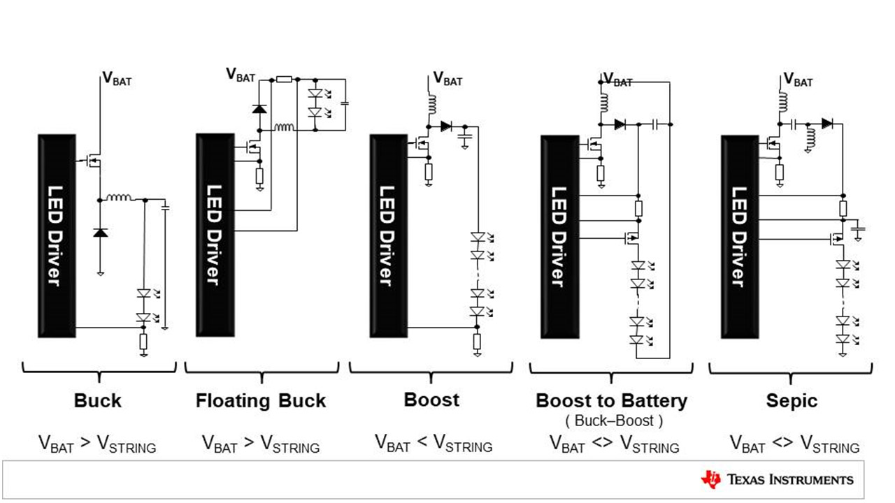
Figure 2 shows basic schematics of common DC/DC LED driver topologies and their voltage relationships.

Figure 2: Basic schematics of common DC/DC LED driver topologies

Except buck LED drivers, which require a high-side metal-oxide semiconductor field-effect transistor (MOSFET), all other topologies can be implemented with a low-side MOSFET controller. Hence, a low-side MOSFET controller is one of the necessary elements to build a flexibly configurable LED driver.

As electronic technology advances and car manufacturers feel more comfortable adding electronic controls to their vehicles, a modern full LED automotive headlight will employ an ECU with a modernized BCM, including microcontrollers (MCUs). The ECU should be able to communicate through the MCU upon receiving commands from the BCM and all headlight functions are controlled accordingly. Figure 3 shows a modern architecture for a full LED automotive headlight.

 Figure 3: Modern architecture for full LED automotive headlight

The MCU in the ECU receives information from the BCM to determine which headlight function to turn on or off. More advanced models might require the ECU to change individual headlight brightness based on BCM commands. It would be best to have an effective digital protocol control, such as SPI, within the ECU such that the MCU can communicate with individual DC/DC LED drivers through the digital interface.

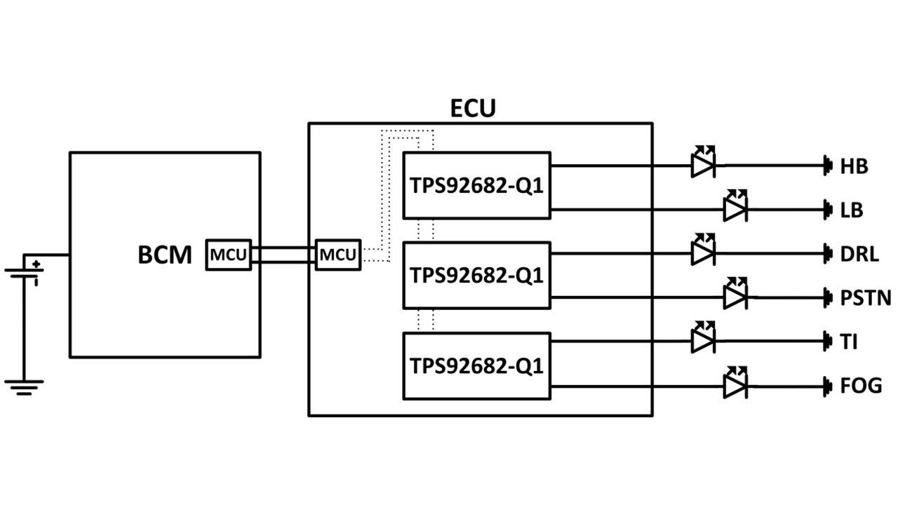
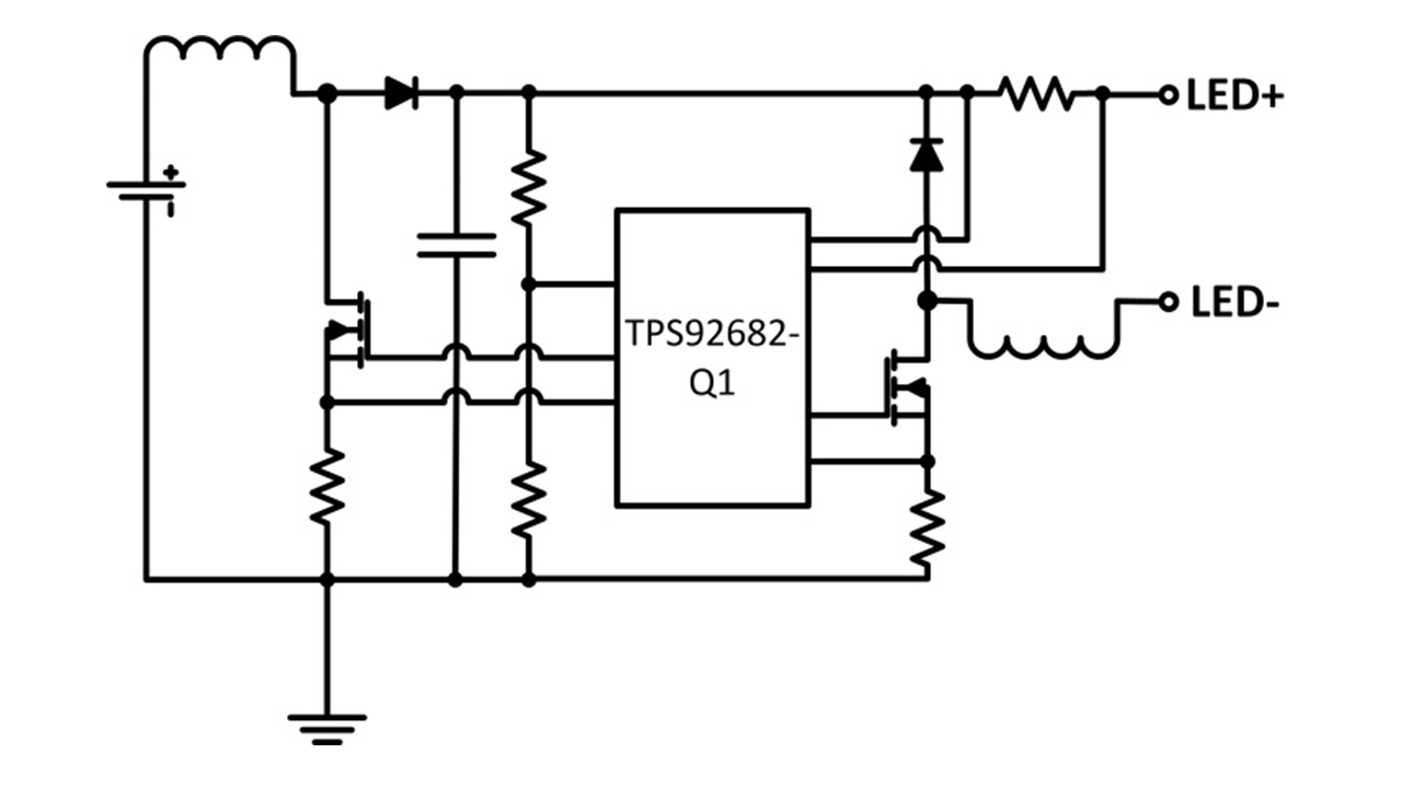
The TPS92682-Q1 is a dual-channel low-side N-type MOSFET controller with Serial Peripheral Interface (SPI) for parametric setup through digital controls. With a low-side N-type MOSFET controller, different DC/DC LED driver topologies can be built, such as boost, boost-to-battery, single-ended primary inductor converter and floating buck. SPI enables the MCU to provide parametric setup information through digital protocols. More importantly, the dual-channel device has two fully independent controllers that can be programmed flexibly according to the ECU’s commands.  As illustrated in Figure 4, it’s possible to build a six-channel ECU with three TPS92682-Q1 devices.

 Figure 4: Six-channel ECU example block diagram with the TPS92682-Q1

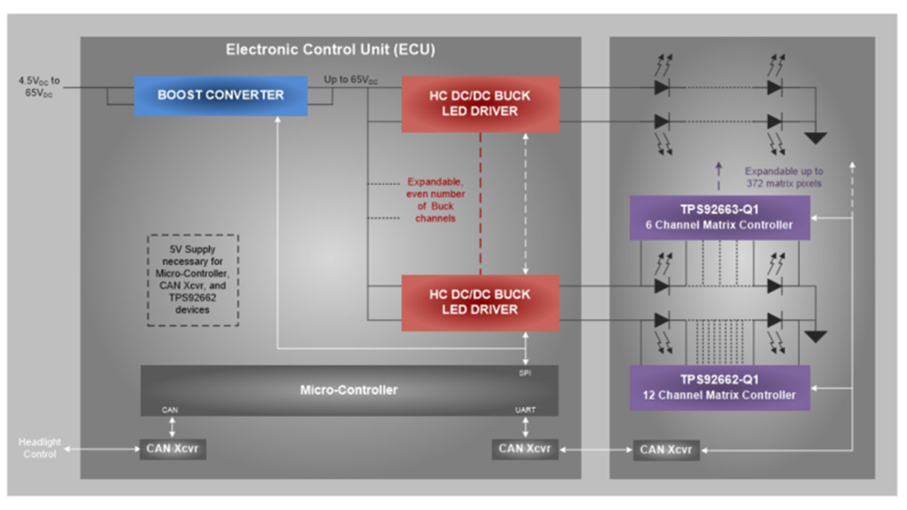
The TPS92682-Q1 has the ability to configure channels to be current output or voltage output. Simple ECUs normally provide current sources to LEDs for different headlight functions. More advanced headlights, such as matrix LED headlights, require that the LED drivers be in a boost-to-buck configuration for pixel brightness control compatibility with LED matrix managers. Figure 5 shows a typical ECU block diagram for an advanced headlight.

Figure 5: Typical ECU block diagram for an advanced headlight

The two channels of the TPS92682-Q1 can be programmed to run as a two-phase voltage-output regulator. This enables high output power – up to 120 W. However, there are simple headlight LED drivers that require a boost-to-floating-buck architecture. By configuring one channel as a boost voltage output with another channel configured as a floating buck current output, it’s possible to configure a simple boost-to-floating-buck LED driver with a single TPS92682-Q1 device. Figure 6 shows a concept schematic of a boost-to-floating buck using the TPS92682-Q1.

Figure 6: Concept schematic of a boost-to-floating buck using the TPS92682-Q1

As automotive headlights move from bulbs, xenon and high-intensity lamps to LEDs, the TPS92682-Q1 helps implement a flexibly configurable automotive headlight ECU that can communicate with a modern BCM.

Additional resource

Selecting TVS diodes in hot-swap and ORing applications

$
0
0

Designers will often use a transient voltage suppression (TVS) diode to clamp large surge currents to a safe voltage level in order to protect nearby components from damage. In many ways, a TVS diode behaves like a Zener diode, but with a higher power-rating capability because of its larger die size and stronger wire bonding.

Why do hot-swap applications need a TVS diode?

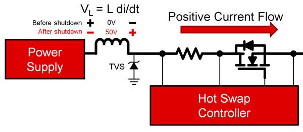
In a hot-swap application, if there is a large overcurrent fault, then the protection integrated circuit (IC) will shut off the current quickly in order to shield nearby components from damage. This fast shutdown of current – from maybe 50 A (overcurrent) to 0 A (shutoff for protection) – can occur within tens of nanoseconds and results in a large current transient (di/dt), as shown in Equation 1:

This current will be trapped as energy inside of trace or wire inductance on the input. Although the trace inductance may be low, at a value of about 10 nH, it will still produce a surge on the input of the hot-swap controller, based on Equation 2:

That -50-V surge will be in series with the input power supply and will effectively create a positive voltage spike on the input rail, often exceeding the voltage rating of the hot-swap controller IC or metal-oxide semiconductor field-effect transistor (MOSFET) drain-to-source voltage (VDS) (see Figure 1). To prevent this voltage surge from occurring, you can place a TVS on the input to divert energy from the inductance straight to ground. The optimal placement of the TVS will be after any series inductance on the input (such as after a fuse).

Figure 1: Inductive kickback after hot-swap controller shutdown. The voltage across the inductor, VL was previously 0 V during normal operation; after fast current shutdown, VL equals 50 V and will be added in series to the input power supply

How do you choose a TVS diode?

The simplest way to pick a TVS diode for a hot-swap application is to choose one that meets the following three criteria:

  • A voltage breakdown, VBR, greater than your maximum power-supply input voltage.
  • A clamping voltage, VC, below the absolute maximum rating of your hot-swap controller IC or MOSFET VDS.
  • A peak pulse current rating, IPP, above the peak current at which the hot-swap controller will shut off. This worst-case value is often the current visible if there is a short circuit on the output and the hot-swap controller shuts off. An accurate value to use would be the peak current measurement on an actual prototype board, with a realistic short circuit applied to the output.

For a 12-V high-power application, a common TVS choice is the 5.0SMDJ12A, which has a 5-kW transient power capability. For a deeper analysis of the equations used in choosing a TVS diode for a hot-swap application, check out the Power Electronics article, “TVS Clamping in Hot-Swap Circuits.”

How to design more noise-tolerant industrial systems

$
0
0

Modern factories and other industrial settings consist of a rich mesh of interconnected machines that themselves include devices such as networked computers, programmable logic controllers, input/output cards, field transmitters, sensors, and a collection of wired and wireless communications networks. The amount of data generated and communicated within factory environments has increased dramatically in the last few years, as companies race to monetize the efficiencies and agility that smart factories bring.

However, connecting factory equipment has unique challenges. One of these challenges is the vast array of electrical noise generated by factory equipment such as motors, switching power supplies, high-voltage distribution cables and other similar sources. A variety of system impairments such as bit errors, signal degradation, signal amplification, signal loss or a combination of these will generate electrical noise, ultimately resulting in system malfunctions that range from unnoticeable bit glitches to catastrophic system failures that could endanger lives or result in the processing of unusable goods.

Industrial system designers must pay special attention to the impact that noise from a factory environment can have on the robustness of their design and create layers of noise protection; for example, implementing system circuit designs that are noise-tolerant in case noise makes its way into a system’s circuits.

Multiple design techniques exist to mitigate and overcome this type of electrical noise; all engineers should use building-block devices like logic circuits, which have a higher level of noise immunity. Logic circuits play a critical role in bringing a system’s circuit components together, and as such act as gateways for control and data signals of a system’s circuit implementations. Using logic devices with higher noise immunity basically means stopping noise at these gateways before it can propagate through a system.

One critical feature of logic devices that helps improve noise immunity is Schmitt-trigger inputs. Standard complementary metal-oxide semiconductor (CMOS) inputs are susceptible to noise: noisy inputs can cross the input threshold multiple times, causing oscillations at the output (as illustrated in Figure 1), potentially resulting in system errors. In contrast, a Schmitt-trigger input design separates the positive and negative-going thresholds.

 Figure 1: Standard CMOS inputs vs. Schmitt-trigger inputs

Logic circuits with Schmitt-trigger inputs have outputs that will switch only once; they will also have clean signal edges for any CMOS input (see this Schmitt-trigger video, “Eliminate slow or noisy input signals,” for a detailed explanation). Given the importance of using logic building-block devices with Schmitt-trigger inputs for noisy industrial applications, logic device selection becomes an important step.

TI’s HCS logic family makes the logic selection process easy for industrial applications by providing a portfolio where every logic device includes Schmitt-trigger inputs. Encompassing all major logic function types, the HCS family enables industrial system designers to confidently implement noise-tolerant and robust system control and data logic interfaces.

Additional resources

Optimizing flip-chip IC thermal performance in automotive designs

$
0
0

Significant decreases in the size of power integrated circuits (ICs) have enabled system designers to achieve reductions in power-supply solution size and cost, which is imperative to furthering the development of advanced systems in the automotive industry. However, one challenge that arises from this trend is impaired thermal performance. Without a thoughtful printed circuit board layout to spread the heat, using smaller ICs in a design might result in a significant temperature rise, which is especially concerning for automotive applications.

One common small-size package is a flip-chip IC. Flip-chip packages have enabled ICs to become even smaller, making them a preferred choice for engineers designing tiny power-supply solutions. This size reduction has further impacted thermal performance, however, and made thermal mitigation even more challenging. In this article, I’ll review the considerations and guidelines for achieving optimal thermal performance with small flip-chip ICs.

The difference between standard wire-bond QFN and flip-chip packages

A typical package like a wire-bond quad flat no-lead (QFN) has a junction/die that typically connects to a thermal pad for heat dissipation, as shown in Figure 1. The junction has bond wires to connect the junction to the pins. The bond wires are very thin and do not conduct heat very well, resulting in most of the heat escaping from the thermal pad.

Figure 1: Junction connections to pins and thermal pad in a standard wire-bond QFN package

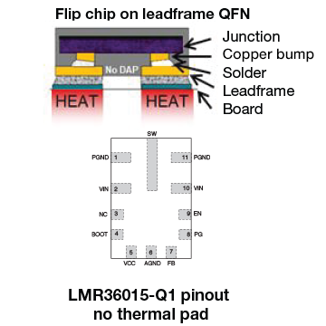
Flip-chip technology flips the chip/junction so that the copper bumps are upside down and soldered directly to the lead frame, as shown in Figure 2. This results in reduced parasitic impedances from the pin to the junction, improving efficiency, size, switch ringing and overall performance for a given specification. The flipped chip, however, prohibits the die from connecting directly to a thermal pad – there is no thermal pad on typical flip-chip devices. Fortunately, the elimination of the bond wires facilitates paths of high thermal conductivity from the die, through the pins and into the board. This results in good thermal conduction between the die and the board, thus removing heat from the IC.

Figure 2: Junction connections to pins for flip-chip devices

Using pins to optimize heat distribution

Power-supply designers can achieve very good thermal performance with flip-chip ICs by connecting and using flip-chip pins for heat distribution. Connecting the pins to large copper traces and polygon pours reduces the thermal resistance and pulls more heat out of the package.

The power ground (PGND) pin is often used to extract heat from the IC. PGND also requires higher current capability; therefore, the copper bump connecting the junction to the PGND pin is typically larger than the copper bump of a signal pin. This larger copper bump allows more heat to flow from the PGND pin(s). On the system side, PGND is electrically quiet, so a large copper surface area will not impact electromagnetic interference (EMI) levels – an important requirement in automotive systems.

You can use other pins for improved thermal performance, but take care not to increase the surface area of noisy nodes such as the switch node and the bootstrap pin, as this can impact EMI performance and may cause violations of EMI test limits.

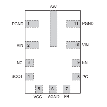
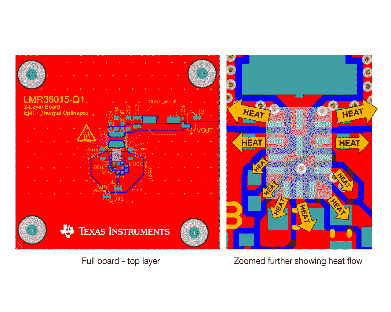
Let’s test these strategies using the LMR36015-Q1, a 150°C-rated, 60-VIN, 1.5-AOUT flip-chip buck converter. Figure 3 shows the pinout of the LMR36015-Q1.

Figure 3: Pinout for the LMR36015-Q1

Figure 4 shows a thermally optimized layout of the LMR36015-Q1. Pins 1 and 11 are PGND pins connecting to a large ground plane, which provides good heat distribution. The layout also uses thermal vias on the ground plane, harnessing the inner layers for even more heat distribution. Pin 6 is analog ground, which also has a large ground plane and thermal vias. Pins 2 and 10 are the input voltage (VIN) pins, which like the PGND pins have large internal copper bumps for increased current capacity and improved thermal conductivity for better heat dissipation. The input voltage on a buck is inherently noisy, however, so watch the size of the VIN plane in order to not push EMI levels past acceptable limits. The switch node and bootstrap pin are noisy due to fast changes in voltage, so it is important to keep those nodes as small as possible.

Figure 4: Sample layout for the LMR36015-Q1 flip-chip IC

The LMR36015-Q1 board measures 2.2 by 2.3 inches (5.6 cm by 5.8 cm) and only has two layers: top and bottom. Typical boards are larger and contain four or more layers, so the size and number of layers increases the thermal challenge. The thermally optimized layout allows the LMR36015-Q1 to operate at 12 VIN, 5 VOUT at a full load of 1.5 AOUT, switching at 400 kHz with a temperature rise of only 28°C in a 22°C still-air environment. This layout allows the 150°C-rated IC to operate in ambient temperatures as high as 115°C, which gives 10°C of margin above the 105°C ambient requirement, which is used in some of the harshest automotive environments.

Smaller-power ICs in flip-chip packages do not necessarily result in poor thermal performance. When compared to wire-bond packages, it is possible to achieve equivalent thermal performance by following the guidance presented in this article.

Additional resources

How to choose the right battery-charger IC for ultrasound point-of-care products

$
0
0
Other Parts Discussed in Post: BQ24610, BQ25713, BQ25790, BQ25792, BQ25892, BQ25895

Advancements in ultrasound imaging technology, along with rising demand for minimally invasive diagnostics and therapeutics, have made it possible to implement ultrasound applications for medical use. For example, employing ultrasound for remote patient monitoring has become increasingly popular given its cost-effective, safe and fast diagnostic capabilities. There is also demand for ultrasound devices to become more portable so that high-quality medical care can be consistently given anywhere from a hospital or doctor’s office to someone’s home or a remote village.

In this article, I’ll examine compact battery-charger integrated circuits (ICs) and solutions for ultrasound point-of-care products that are used by medical professionals to diagnose problems wherever a patient is receiving treatment.

Types of point-of-care ultrasound devices and charging requirements

There are three major types of ultrasound devices: cart-based, notebook and handheld. System power consumption varies among the three. As a result, they need different battery configurations.

As shown in Figure 1, a cart-based ultrasound machine is the most powerful of the three types. The maximum system current can be as high as 20 A at 12 V. The cart typically includes four individual battery packs connected in parallel to supply the system load sufficiently. Each battery pack is configured with four or more cells in series.

Because of air traffic control regulations on lithium-based batteries, the capacitance of each battery pack cannot exceed 100 watt-hours. As a result, the four battery packs cannot be tied directly together. Each individual pack needs its own charging and discharging path, as illustrated in Figure 2.

Figure 1: Point-of-care ultrasound devices (cart-based, notebook and handheld)

Figure 2: A simplified multi-battery pack battery-management system

Notebook-based devices also have a maximum battery capacity limitation of 100 watt-hours. System power consumption of an ultrasound notebook can go as high as 10 A at 12 V. Therefore, this type of machine typically includes two individual battery packs with separate charge and discharge paths.

The handheld smart probe is much smaller in size; it only collects and transmits data. Therefore, a single battery pack of one to two lithium-ion or lithium-polymer cells in series is sufficient to support operation. Unlike cart- or notebook-based ultrasound devices, where the battery is used as backup power source, the battery in a smart probe is the main power source. Thus, fast charging with USB Type-C® Power Delivery, for example, is required for daily use.

Battery charger recommendations

Again, for cart-based and notebook devices, the battery serves as a backup and the line power is the main power source. Because of the high system current in these applications, you can use a direct power path where the system is powered by the input source directly. When the input source is removed, the direct power-path management automatically powers the system load from the battery.

TI’s BQ24610 is a stand-alone battery-charge controller with direct power-path charging for up to six lithium-ion or lithium-polymer cells in series. The stand-alone feature makes charging parameters easily configurable through resistors.

For an ultrasound notebook, which can have multiple types of input sources that vary from 12 V to 24 V, the BQ25713 buck-boost charger can enable charging from different input sources without an additional DC/DC converter in front of the charger input.

For the most compact ultrasound device, the smart probe, an integrated buck-boost charger like the BQ25790 offers a smaller solution size with high integration and chip-scale packaging. The device supports one to four cells in series and up to 5 A of battery current for fast charging. The input voltage range of 3.6 V to 24 V supports the full range for USB Type-C® Power Delivery. It also features a dual-input control that toggles between two power sources, such as wireless power or USB. Part of the same family of battery charger ICs, the BQ25792 comes in a quad flat no-lead (QFN) package to offer better thermal performance.

For devices with one-cell configuration only, the BQ25892 or BQ25895 buck chargers can also be a good option, with a high charge-current capability up to 5 A. The D+/D- function detects standard USB ports and adjustable high-voltage adapters as input power sources.

As portability in ultrasound devices becomes more central when providing quality point-of-care patient diagnostics, you must optimize your battery designs. Different power levels require different battery design configurations, so it’s important to understand your system and charging requirements in order to select the best battery charger integrated circuit.

Additional resources


Monitoring 12-V automotive battery systems: Load-dump, cold-crank and false-reset management

$
0
0
Other Parts Discussed in Post: LM5060-Q1

The 12-V lead-acid battery is a staple in automotive electronic systems such as automotive cockpits, clusters, head units and infotainment. Monitoring the battery voltage is necessary in order to maintain and support the power requirements of the modern vehicle. Although automotive batteries can withstand wide voltage transients that exceed their nominal voltage during load-dump and cold-crank conditions, what is considered an acceptable operating voltage range changes, and each automotive manufacturer has their own specification that goes beyond the International Organization for Standardization (ISO) 26262 standard. In this technical article, I’ll go over how to manage load-dump and cold-crank conditions, and how to use hysteresis to prevent false system resets.

Managing transients during load-dump conditions

An automotive 12-V battery is nominally specified to operate between 9 V and 16 V. Variations outside of this range increase during conditions known as load dump and cold crank. The ISO 26262 standard, a functional safety standard for automotive electric and electronic systems, describes the expected range of these voltages.

In the load-dump event illustrated in Figure 1, the alternator, designated with the letter A, is abruptly disconnected from the battery because of mechanical vibration, a loose terminal or corrosion at the terminal. The event can cause a battery-voltage transient as high as 60 V for nearly 500 ms.

Figure 1: Load-dump and transient characteristics

Automotive manufacturers can implement overvoltage protection, which will disconnect vital systems from a load-dump event; see Figure 2. Setting a trip point will disconnect the supply source from the electronic subsystem and reconnect the supply after a fixed delay, once the transient voltage settles within a normal operating range. A high-side protection controller such as the LM5060-Q1 needs a disable and enable external signal, which may require a complex design that includes discrete components or a microcontroller.

High-voltage supervisors such as the TPS37A-Q1 and TPS38A-Q1 operate up to 65 V, simplifying designs by directly connecting to the battery and withstanding a load-dump transient voltage. The TPS37A-Q1 and TPS38A-Q1 also give automotive manufactures flexibility by providing a programmable reset delay through an external capacitor, which delays the turn-on of the LM5060-Q1, thus helping protect downstream subsystems from an overvoltage event by allowing an additional reset delay time for the supply voltage to settle.

Figure 2: An overvoltage protection circuit

Effectively dealing with cold-crank conditions

During cold-crank, the starter draws more current and pulls the battery voltage down, sometimes as low as 3 V for 15 ms. Cold-crank conditions are occurring more frequently in modern automobiles as manufacturers adopt systems such as start-stop, a hybrid design that disengages the combustion engine when the vehicle is not in motion (stopped at a traffic light, for example) to improve fuel economy. Start-stop functionality necessitates continuous monitoring of the battery voltage while consuming the least amount of power to ensure that the downstream system is properly initialized and devices remain in a valid state. The TPS37A-Q1 and TPS38A-Q1 voltage supervisors are a good fit for cold-crank conditions because their minimum operating voltage is 2.7 V; additionally, their maximum quiescent current of 2 µA helps manufacturers minimize power losses.

Using hysteresis to prevent false resets in a system

Despite the nominal operating range of 9 V to 16 V, automotive manufacturers specify their own “out of operating voltage range” limits for automotive batteries. Most voltage supervisors used for monitoring have a narrow operating range (i.e. 3 V to 5 V) within those limits, necessitating the use of multiple devices or discrete circuits to implement a monitoring circuit that can properly detect both undervoltage and overvoltage limits.

Preventing false resets requires hysteresis at both the upper and lower boundaries; look for devices with factory-programmable voltage threshold hysteresis that offer the flexibility to monitor the voltage rail through the VDD pin (or a dedicated SENSE pin when a voltage rail is higher or lower than VDD). A lack of integrated circuit hysteresis management will require the implementation of discrete components to ensure system robustness, but that increases both system size and cost.

Both the VDD and SENSE pins provide hysteresis to prevent false resets in a system where the monitored rails can fluctuate as voltage varies from various load sources. Hysteresis plays a critical role in providing a stable system in the event that the supply voltage spikes or dips in a response to a vehicle operational condition. For instance, when a driver turns on the air conditioning, the voltage can spike or dip momentary, which can trigger a false reset.

Conclusion

Voltage monitoring ensures that critical systems in modern vehicles are operating safely. By operating directly from the battery and providing the necessary control logic to protection circuitries, high-voltage supervisors offer many benefits, including an effective way to manage load-dump and cold-crank conditions, as well as a reliable way to prevent false system resets. In addition, their separate VDD and SENSE pins can help address redundancy to create a highly reliable system.

Additional resources

How to reduce EMI and shrink power-supply size with an integrated active EMI filter

$
0
0
Other Parts Discussed in Post: LM25149-Q1 This technical article is co-authored by Tim Hegarty Design engineers working on low-electromagnetic interference (EMI) applications typically face two major challenges: the need to reduce the EMI of their de...(read more)

How to choose the right LDO for your satellite application

$
0
0
Other Parts Discussed in Post: TPS7H1101A-SP

Radiation-hardened low-dropout regulators (LDOs) are vital power components of many space-grade subsystems, including field-programmable gate arrays (FPGAs), data converters and analog circuitry. LDOs help ensure a stable, low-noise and low-ripple supply of power for components whose performance depends on a clean input.

But with so many LDOs available on the market, how do you choose the right radiation-hardened device for your subsystem? Let’s look at some design specifications and device features to help you with this decision.

Dropout voltage for space-grade LDOs

An LDO’s dropout voltage is the voltage differential between the input and output voltage, at which point the LDO ceases to regulate the output voltage. The smaller the dropout voltage specification, the lower the operating voltage differential one is able to operate with, which results in less power and thermal dissipation as well as inherently higher maximum efficiency. These benefits become more significant at higher currents, as expressed by Equation 1:

LDO power dissipation = (VIN-VOUT)xIOUT                 (1)

In the radiation-hardened market, it can be difficult to find truly low dropout regulators that offer strong performance over radiation, temperature and aging. TI’s radiation-hardened LDO, the TPS7H1101A-SP, is one example, offering a typical dropout voltage (Vdo) of 210 mV at 3 A – currently, the lowest on the market. If you have a standard 5-V, 3.3-V, 2.5-V or 1.8-V rail available, this LDO can regulate output voltages down to 0.8 V to supply any required voltage, as well as the current needed for one or more space-grade analog-to-digital converters (ADCs) or clocks.

Noise performance for space LDOs

With satellites in space for 10 or more years, getting the maximum performance out of the onboard integrated circuits helps ensure design longevity. In order to provide a clean, low-noise rail for high-performance clocks, data converters, digital signal processors or analog components, the internal noise generated by the LDO’s circuitry needs to be minimal. Since it is not easy to filter internally generated 1/f noise, look for LDOs with inherent low-noise characteristics. Lower-frequency noise is often the largest and most difficult to filter out. The TPS7H1101A-SP offers one of the lowest 1/f noise levels, with a peak around 1 µV/Hz at 10 Hz. See Figure 1 below for RMS noise over frequency.

Figure 1: TPS7H1101A-SP noise

PSRR for space LDOs

The power-supply rejection ratio (PSRR) is a measure of how well an LDO can clean up, or reject, incoming noise from other components upstream. For higher-end ADCs, the input supply noise requirements continue to get tighter to minimize bit errors. At higher frequencies, it is difficult to have high PSRR given the characteristics of the control loop. Often, designers need to use external components to filter the noise to reach an acceptable effective PSRR, which increases solution size – an obvious issue for space applications, where size and weight tie directly to satellite launch costs. The PSRR is most important at the switching frequency of the upstream supply (since there is a voltage ripple at this frequency). Additionally, PSRR is important above this frequency because of the switching harmonics. If you’re looking for good PSRR, the TPS7A4501-SP LDO offers a PSRR of over 45 dB at 100 kHz.

Other important LDO features

Outside of dropout voltage, PSRR and noise, let’s look at several smart features that can be integral to the performance of a radiation-hardened LDO.

  • Enable. In space, there is only a set amount of power available from the solar panel, from which many functions need to run. The enable feature allows you to specify whether the LDO should be on or off at any given time, and proves critical for overall savings in a power budget. The enable pin is also important for power-up sequencing, which is of increasing need in newer-generation FPGAs.
  • Soft start. A voltage that rises too quickly can cause current overshoot or an excessive peak inrush current, damaging downstream components such as the FPGA or ADC. The soft-start feature regulates how quickly the output voltage rises at startup. Soft start also prevents a level of voltage droop that could be unacceptable by preventing an overcurrent draw on the upstream supply.
  • Output voltage accuracy. Often, newer space-grade FPGAs such as the Xilinx KU060 have strict input-voltage tolerance requirements on each rail to enable their best performance. To ensure that your design meets strict accuracy requirements over radiation exposure and end-of-life conditions, look for devices like the TPS7H1101A-SP, which is on the KU060 development board.
  • Size. Other than having a small, easy-to-layout package, other ways to reduce solution size include limiting the number of external components to the LDO; having more integrated features, better PSRR and noise specifications; and more reliable radiation performance under single-event effects. TI’s TPS7A4501-SP is one of the industry’s smallest radiation-hardened LDOs, both in package size, layout and solution size.

Conclusion

With so many options available, it can be difficult to pick the right LDO. Consider which capabilities and features are the most important. For example, if your application is powering a high-end FPGA or high-speed data converter, features like output-voltage accuracy, reference accuracy, PSRR and noise might be the priorities. If, however, you are designing a low-performance analog circuit or working with an older FPGA where tolerance requirements are not so stringent, having the smallest-sized, lowest-cost solution while retaining good-enough capability might be the better option.

Additional resources

Introduction to EMI: Standards, causes and mitigation techniques

$
0
0
Other Parts Discussed in Post: LM5156-Q1, LM62440-Q1, LM25149-Q1

Electronic systems in industrial, automotive and personal computing applications are becoming increasingly dense and interconnected. To improve the form factor and functionality of these systems, diverse circuits are packed in close proximity. Under such constraints, reducing the effects of electromagnetic interference (EMI) becomes a critical system design consideration.

Figure 1 shows an example of such a multi-functional system, an automotive camera module, where a 2-megapixel imager is packed in close proximity with a 4-Gbps serializer and a four-channel power-management integrated circuit (PMIC). A byproduct of the ensuing increase in complexity and density is that sensitive circuitry like the imager and signal-processing elements sit very close to the PMIC, which carries large currents and voltages. This placement inevitably leads to a set of circuits electromagnetically interfering with the functionality of the sensitive elements – unless you pay careful attention during design.

Figure 1: Automotive camera module

Electromagnetic interference (EMI) can manifest itself in two ways. Consider the case of a radio connected to the same power supply as a motor drill, as shown in Figure 2. Here, the operation of the sensitive radio system is affected through conductive means by the motor, since they both share the same outlet for power. The motor also affects the functionality of the radio through electromagnetic radiation that couples over the air and is picked up by the radio’s antenna.

When end-equipment manufacturers integrate components from various sources, the only way to guarantee that interfering and sensitive circuits can coexist and operate correctly is through the establishment of a common set of rules that sets limits for the interfering circuits to be within and which the sensitive circuits need to be capable of handling.

 Figure 2: Electromagnetic interference caused by conducted and radiated means


Learn more about time-saving and cost-effective innovations for EMI reduction in power supplies Read the white paper now 


Common EMI standards

Rules designed to limit interference are established in industry-standard specifications such as Comité International Spécial des Perturbations Radioélectriques (CISPR) 25 for the automotive industry, and CISPR 32 for multimedia equipment. CISPR standards are critical for EMI designs, as they dictate the targeted performance of any EMI mitigation technique. CISPR standards are categorized into conducted and radiated limits depending on the mode of interference, as shown in Figure 3. The bars in the plots in Figure 3 represent the maximum conducted and radiated emission limits that the device under test can tolerate when measured using standard EMI measuring equipment.

 Figure 3: Typical standards for conducted and radiated EMI

Causes of EMI

Building systems compatible with EMI standards requires a clear understanding of the primary causes of EMI. One of the most common circuits in modern electronic systems is the switch-mode power supply (SMPS), which provides significant improvements in efficiency over linear regulators in most applications. But this efficiency comes at a price, as the switching of power field-effect transistors in the SMPS causes it to be a major source of EMI.

As shown in Figure 4, the nature of switching in the SMPS leads to discontinuous input currents, fast edge rates on switching nodes and additional ringing along switching edges caused by parasitic inductances in the power loop. While the discontinuous currents impact EMI in the <30-MHz bands, the fast edges of the switching node and the ringing impact EMI in the 30 to 100 MHz and >100-MHz bands.

 Figure 4: Main sources of EMI during operation of an SMPS

Conventional and advanced techniques to mitigate EMI

In conventional designs, there are two main methods for mitigating the EMI generated by switching converters, both of which have an associated penalty. To deal with low-frequency (<30-MHz) emissions and meet appropriate standards, placing large passive inductor-capacitor filters at the input of the switching converters leads to a more expensive, less power-dense solution.

Slowing down the switching edges through the effective design of the gate driver typically mitigates high-frequency emissions. While this helps reduce EMI in the >30-MHz band, the reduced edge rates lead to increased switching losses and thus a lower-efficiency solution. In other words, there is an inherent power density and efficiency trade-off to achieve lower EMI solutions.

To resolve this trade-off and obtain the combined benefits of high power density, high efficiency and low EMI, a host of techniques as shown in Figure 5 are designed into TI’s switching converters and controllers, such as LM25149-Q1, LM5156-Q1 and LM62440-Q1. These techniques such as spread spectrum, active EMI filtering, cancellation windings, package innovations, integrated input bypass capacitors, and true slew-rate control methodologies are tailored to specific frequency bands of interest and are described in depth in the white paper linked above and related instructional videos linked in the additional resources section.

 Figure 5: Techniques designed into TI’s power converters and controllers to minimize EMI

Conclusion

Designing for low EMI can save you significant development cycle time while also reducing board area and solution cost. TI offers multiple features and technologies to mitigate EMI. Employing a combination of techniques with TI’s EMI-optimized power-management devices ensures that designs using TI components will pass industry standards without much rework. I hope this information and related content will simplify your design process and enable your end-equipment to remain under EMI limits without sacrificing power density or efficiency.

Additional resources

Improving industrial radar RF performance with low-noise, thermal-optimized power solutions

$
0
0
Other Parts Discussed in Post: IWR1843, IWR6843, LP87702, LP87702-Q1

For years, passive infrared sensors and lasers have sensed remote objects or measured range in applications such as robotics, level sensing, people counting, automated doors and gates, and traffic monitoring. But with demand for higher precision and resiliency against environmental influences such as bad light, harsh weather conditions and extreme temperatures, it is inevitable that millimeter-wave (mmWave) radar technology will take over.

mmWave technology provides ultrawide resolution, better calibration and monitoring, and highly linear signal generation for accuracy in radio-frequency (RF) sensing. These benefits enable the detection of objects in otherwise obstructed views for intelligent safety in forklifts and drones, and enhance sensing performance that improves power in intelligent streetlights and perimeter security.

For autonomous guided vehicles (AGVs) and collaborative robots (cobots) in industrial automation, mmWave technology offers not just high accuracy but preserves safety by helping avoid collisions of AGVs with other objects or human accidents caused by cobots.

The low noise and thermal performance of a radar’s power solution also plays a major role in its ability to sense, image and communicate the range, velocity and angle of remote objects with high accuracy.

In this article, I’ll discuss power-supply design challenges that are applicable to any radar processor in the industry, using the 60- to 64-GHz IWR6843 and 76- to 81-GHz IWR1843 mmWave radar sensors as examples.

Let’s begin with the most important power specifications and how you can best meet those parameters.

Tight ripple specifications

Ripple is an unwanted side effect of switching regulators that is normally suppressed by the design architecture or output filter selection. Ripple directly affects the output voltage accuracy and noise level, and thus the RF performance of the system.

The RF rails of a radar processor are sensitive to supply ripple and noise because these supplies feed blocks in the device such as the phase-locked loop, baseband analog-to-digital converter and synthesizer. The IWR6843 and IWR1843 processors have RF rails (1 V and 1.8 V) with very tight ripple specifications in the microvolt range. It’s common practice to use low-dropout regulators on RF rails because of low noise, but high-current LDOs (>1 A) are costly and depreciate the system’s thermal performance.

In order to meet low ripple specifications, I recommend using regulators with a high switching frequency, which will enable you to select smaller passive components (inductors, output capacitors) in the design architecture and achieve the necessary ripple amplitude.

Figure 1 shows the output ripple performance of TI’s LP87702 device, which integrates two step-down DC/DC converters switching at a high frequency (4 MHz) and meets the ripple specs of the IWR6843 RF rail without the use of LDOs. The LP87702 supports spread-spectrum switching frequency modulation mode, which further helps reduce both the switching frequency spur amplitude and electromagnetic interference spurs.

Figure 1: The LP87702’s 1-V ripple performance against IWR6843 ripple specifications, with a low-cost second-stage inductor-capacitor (LC) filter using MPZ2012S101A ferrite

Optimized thermal performance

The miniaturizing of devices has increased the heat generated per unit area in printed circuit boards; mmWave radar designs are no exception. For compact radar applications such as automatic lawn mowers or drones that also have plastic housing, thermal management becomes a priority; increased board temperatures not only reduce mmWave sensor lifetimes but also affect RF performance.

The major contributors for thermal dissipation in a radar power architecture are high-current LDOs, which add significant (>1 W) heat to the system and also affect RF performance. Plus, high-current LDOs are not only expensive; they require a heat sink, adding more cost to the system. Designing the power architecture of a radar system without LDOs prevents them from deteriorating a system’s thermal performance and increasing the overall cost and solution size from external components.

Figure 2 shows how the LP87702 integrated power-management integrated circuit (PMIC) and external DC/DC step-down regulator can power all of the RF rails of the IWR6843 or IWR1483 processor. The 5-V rail from the integrated boost supports the Controller Area Network-Flexible Data Rate interface, typically required in AGVs and industrial robots.

Figure 2: IWR6843 or IWR1843 power block diagram

A two-IC solution distributes hot spots and removes the need for an external heat sink, reducing overall system cost. The integrated 4-MHz buck converters (Buck 0 and Buck 1) eliminate the need for high-current LDOs, thus improving overall efficiency and thermal performance while meeting the IWR6843 noise performance with a low-cost LC filter.

The LP87702 device also includes a protection feature against overtemperature by setting an interrupt for the host processor.

Industrial functional safety

Industrial functional safety standards are more important than ever, as humans are increasingly interacting with autonomous robots, safety scanners in factory automation settings, automated pedestrian doors, and industrial doors and gates. These systems must be able to detect anomalies and react accordingly.

TI’s LP87702-Q1 dual buck converter supports functional safety requirements up to Safety Integrity Level (SIL)-2 at the chip level, which are specified for end equipment such as AGVs and industrial robots. By integrating two voltage-monitoring inputs for external power supplies and a window watchdog, the LP87702-Q1 helps reduce system complexity and eliminates the need for an additional safety microcontroller. By providing chip-level compliance, the LP87702-Q1 also helps streamline time to market.

SIL risk levels are determined by International Electrotechnical Commission (IEC) 61508, an international standard to help ensure safe operations between human and robotic interaction, including cobots.

Conclusion

Although LDOs offer a low-noise option for powering the RF rails of a radar processor, they can complicate overtemperature considerations, SIL compliance and system designs, and require additional components. Consider PMICs, which offer better thermal performance and ease of design.

Additional resources

Viewing all 437 articles
Browse latest View live


<script src="https://jsc.adskeeper.com/r/s/rssing.com.1596347.js" async> </script>