Quantcast
Channel: Power management
Viewing all 437 articles
Browse latest View live

Improve circuit breaker leakage current response with a voltage supervisor

$
0
0

A residual current detector (RCD) or residual current circuit breaker (RCCB), detects leakage currents when an alternate path to ground is established. RCDs isolate the power source from the leakage path by tripping open the circuit. Unlike fuses, these types of circuit breakers can be reset and reused. They play an important role in protecting people and equipment.


In this post, I will review the requirements for leakage current detection and tripping for RCDs and how ultra-low power voltage supervisors or Reset IC can be used as a leakage current detector. I will also explain how voltage supervisors benefits medium-voltage breakers, such as air-circuit-breaker (ACB) and molded-case-circuit-breakers (MCCB) that use a microcontroller.


Using a voltage supervisor as a leakage current threshold detector

Leakage currents occur when an alternate path is established by a malfunctioning device or by a person unintentionally touching the line, creating an alternate path to ground. Since long exposures to high leakage currents result in bodily harm, RCDs are designed to respond to currents as low as 5 mA, all the way up to 500 mA. As described in the International Electrotechnical Commission TS60479-1 standard, humans exposed to 50 mA for 200 ms will have muscle contraction; exposures longer than 3 s will increase the probability of ventricular fibrillation.

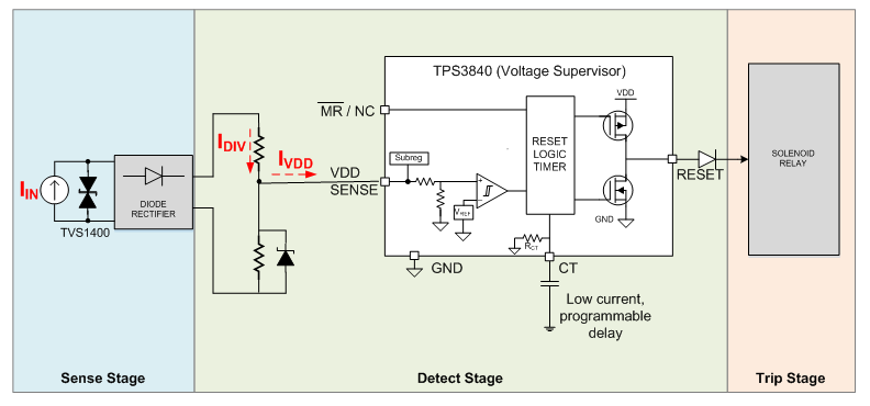
An RCD detects leakage current by sensing the difference between the active line and neutral current. If the line current and the neutral current are not balanced and the leakage current exceeds a pre-determined threshold, the circuit breaker trips, interrupting and isolating the power source. RCD equipment can be broken into three main stages. First is the sensing stage during which a leakage sensor senses the leakage current. In the second stage, the detect circuit sets the leakage current threshold. In the final third stage, a solenoid relay trips open a switch to isolate the leakage from the source.

In the past, electromechanical devices were used as the detect circuit to set the leakage current threshold. Modern RCDs use integrated circuits such as a voltage supervisor to improve the accuracy and response time for detecting leakage current and driving a solenoid relay.

Figure 1 shows how TI’s TPS3840 voltage supervisor can detect leakage current. In this example, the leakage sensor such as a differential current transformer or a zero phase current transformer is represented by a current source. For the current detect circuit a resistor divider is used to convert the input current to a voltage, which is then detected by the TPS3840. The TPS3840 integrates a precise reference voltage band gap and voltage comparator. The trigger point is accurately programmed at the factory by one-time nonvolatile memory (OTP), and the voltage threshold can be set from 1.6 V to 4.9 V within 1% typical accuracy.

When the voltage at the VDD pin rises above the threshold, the RESET pin pulls high to interrupt a microcontroller or drive a solenoid relay. In addition, RESET response time can be extended with a single external capacitor to meet varying RCD response times based on the magnitude of the leakage current.

Figure 1: A voltage supervisor used as a leakage current detector in the Nano power, wide VIN (12-V max) supervisor reference design used as a comparator or power sequencer

The voltage supervisor in this reference design meets three key specifications:

  • Fast power-up and programmable response times. When a voltage supervisor ramps up from a zero input voltage to above the trip point or threshold voltage, it takes a certain amount of time for it to start and react. Circuit breakers need to quickly detect the leakage current level and have flexibility in configuring the response time to trip based on leakage level and duration to avoid nuisance tripping caused by transients. With a startup time of 200 µs, the TPS3840 can quickly respond.

  • Ultra-low input current. In Figure 1, the power pin for the supervisor IC (VDD) is same as the input signal monitoring pin (SENSE). Since it is powered from the input signal, the voltage supervisor should have high input impedance to minimize the error (IIN) on the voltage divider (IDIV). The TPS3840 voltage supervisor consumes ultra-low current and has a typical IQ of 350 nA,

  • Low VPOR for low VOL. VPOR is the minimum input voltage required for a controlled output state. When VIN< VPOR, the output tracks the input and may trigger the relay. VPOR should be as low as possible to provide a margin between the relay’s enable voltage level and voltage supervisor low output voltage level (VOL). The TPS3840 push-pull active-low version has both low VPOR and a VOL of 300 mV to avoid a false reset.

Using a voltage supervisor as a microcontroller supply voltage monitoring

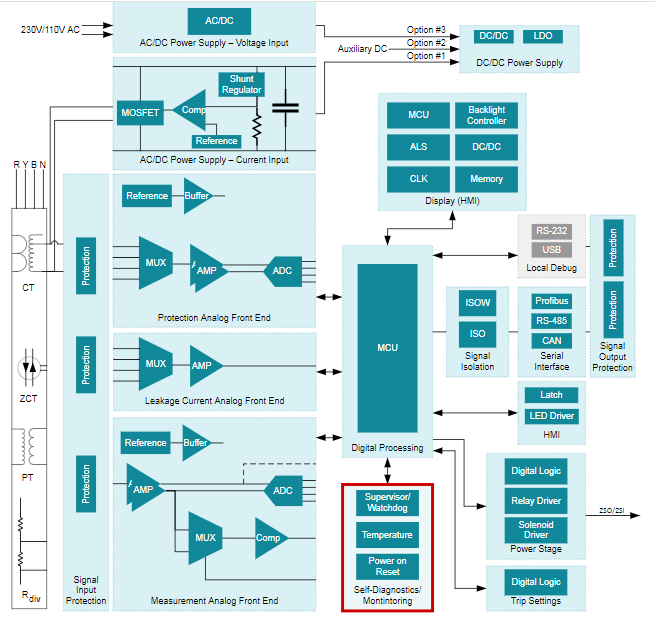
Figure 2 shows a block diagram of ACB and MCCB reference design, these circuit breakers require microcontrollers to process captured data to detect overcurrent and ground current faults. A low IQ voltage supervisor such as the LM8364 or TPS3840 can monitor the power rails. The TPS3840 has a wider operating temperature range and lower IQ than LM8364.

If the voltage supervisor is integrated in the microcontroller then an external watchdog timer is recommended. An external watchdog helps ensure that the microcontroller does not latch by periodically detecting pulses sent by the microcontroller’s general-purpose input/output pin. If the software glitches and a pulse is missed, the external watchdog timer will reset the microcontroller.

The TPS3430 programmable watchdog timer is a good option, since it offers programmable watchdog timeout and reset time delay to meet the timing requirements of any microcontroller. If enhanced reliability is required then both voltage supervisor and watchdog should be implemented, the TPS3823 integrated watchdog and voltage supervisor is a good alternative, offering fixed threshold and watchdog timeout options.

Figure 2: Signal Processing Subsystem and Current Input Based Self Power for Breaker Applications (ACB/MCCB) reference design block diagram

Voltage supervisors can help enhance your circuit breaker designs by not only monitoring the microcontroller’s voltage supply to ensure normal operation, but also serving as a leakage current detector.

Additional resources


Voltage supervisor requirements for e-meter applications

$
0
0

Introduction

As the electricity grid around the world becomes smarter over time, complex electronic designs are necessary. At the same time, long-term system reliability cannot be compromised. A smart e-meter monitors various system voltages to prevent unexpected conditions that cause inconsistent measurements or system failures.


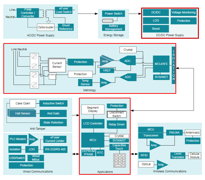
The generic e-meter application shown in Figure 1 consists of several blocks that work together to measure consumed electricity.

  Figure 1: E-meter system block diagram example


This post explains the purpose of the DC/DC power supply, metrology and applications blocks (outlined in red) and dives deep into the importance of the supply voltage supervisor/watchdog timer subsystem. From a general design perspective, a system that monitors electricity consumption needs to be precise, compact and reliable.


DC/DC power supply subsystem requirements: wide VIN and low IQ

An e-meter typically receives 12 V to 24 V from the main AC power supply before converting it into a 3.3-V or 5-V DC voltage to power the rest of the system. A voltage supervisor ensures that the main power supply and all power rails are within the system requirements so that the system operates correctly. If the voltage in this block fails or browns out, the voltage monitoring solution needs to flag the fault condition so that the rest of the system can shut down properly.


If the main power supply does not provide enough power, a switch will connect a backup battery or supercapacitor into the system to provide the required power temporarily. In general, systems that rely on backup power reserves can benefit from any power savings in such critical operating conditions, since lower-power systems will last longer on the power reserves. The DC/DC power-supply block requires a voltage supervisor that has a wide VIN to monitor up to 24 V, and low power when using the power reserves.


Metrology and applications subsystem requirements: high accuracy and programmable delay

The metrology block connects to the outside world through sensors, and is responsible for the actual electricity measurements before sending the information to a microcontroller (MCU) for processing. The applications block has another MCU that formats and stores data in addition to displaying information. This block is responsible for monitoring the whole system and serves as the main interface between the system and the data output.


Accurately monitoring the voltage rails powering the MCUs and MCU activity is critical in these blocks to ensure reliable and consistent measurements. If the MCU is not in the correct operating condition, a voltage supervisor or watchdog timer can flag a fault before any other issues arise. When monitoring a voltage, specifically in a system that requires precise, robust and reliable measurements, voltage monitoring accuracy is important to determine quickly and exactly when the system is not functioning at optimal performance.


Additionally, whenever an application uses an MCU or several different peripherals, there may be the need for programmable startup delay for sequencing purposes. Programmable delay serves an important function when the MCU or other peripherals need a specific amount of time to boot up or to accomplish a task before the system can begin functioning normally. Also, when a fault condition occurs, there may be a need for a specific reset delay for the MCU and/or peripherals to accomplish a task before releasing the reset. In this case, the programmable delay feature provides a programmable and simple solution to add flexibility.


Review of e-meter design requirements

All three of the blocks outlined in Figure 1 require voltage supervisors with a wide VIN, low power, high accuracy and programmable delay. A good option to consider is the TPS3840, as it offers a balance of these requirements in one device.


The TPS3840 has a wide input voltage range up to 24 V or higher with external resistors for monitoring the high- and low-voltage rails, 1% typical voltage monitoring accuracy, and only consumes 350 nA of power while offering programmable delay. In addition, the TPS3840 provides significant precision and flexibility that is not obtainable with internal analog-to-digital converter monitoring in the MCU alone. Compared to the internal ADC monitoring in the MCU, the TPS3840 has more flexibility in the voltage monitor threshold options, a lower power-on-reset voltage and a quicker startup delay.


Power-on reset is defined as the minimum input voltage before the output becomes defined, which is essential for preventing glitches that can produce false faults or premature system startup. The startup delay for the TPS3840 is only 220 µs, meaning that the TPS3840 can begin monitoring voltage before the rest of the system even powers up. Overall, voltage supervisors ensure proper system functionality by continuously monitoring the voltage rails going in to power the internals of an e-meter.


An external watchdog timer in both the metrology and applications blocks will ensure that the MCU does not latch or glitch periodically by detecting pulses sent by the MCU’s general-purpose input/output pin. If the software glitches and a pulse is missed, the external watchdog timer will reset the MCU.


The TPS3430 programmable watchdog timer is a good option since it offers programmable watchdog timeout and watchdog reset delay to meet the timing requirements of any MCU. If you need both a voltage supervisor and watchdog feature, TI has many devices that fit this need. Review the “Voltage Supervisors Quick Reference Guide under the Supervisor + Watchdog Timer heading for all options.


Additional resources

How a small SOT563 DC/DC converter supplies multirail power in industrial applications

$
0
0

Hardware design engineers are forever looking for new solutions for their design tasks. But they are also under time constraints to solve all of the challenges of a new project: always smaller, always more functionality, always lower cost, and with a reliable, well-engineered and tested board.

More and more supply rails are required for power supplies in industrial programmable logic controller (PLC) systems with central processing units, input/output and communication modules, or human machine interface (HMI) panels. Board space is running out quickly.

Small-outline transistor SOT23 is a common package type for DC/DC converters in such applications; however, it consumes a relatively large amount of area on the board. With more than 8 mm2 of package and inductors at 4 mm by 4 mm or larger, the available board space in an industrial system is limiting the number of power rails that you can implement. Moving to an ultra-fine-pitch ball-grid array or chip-scale package is often cost-prohibitive in mass production, and comes with soldering and bench-testing challenges.

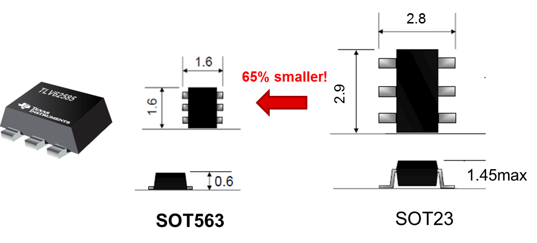
SOT563 combines the advantages of a leaded package with a very small size (Figure 1). It is not a new package for semiconductors. Available for several years for discrete components like metal-oxide semiconductor field-effect transistors, diodes or temperature sensors, it is now also available for DC/DC converters. The SOT563 package is 65% smaller than the ubiquitous SOT23 while still offering leads (pins) accessible to a probe (tester). In addition, these leads enable the use of low-cost mass-production facilities with visual inspection instead of the more complex X-ray checking of the soldering.

Figure 1: TI’s 3-A-output TLV62585DRL in the SOT563 DC/DC converter package

The SOT563 package’s small solution size makes it a good fit for multirail power supplies in HMI or PLC systems. You can place the voltage rails onto the board where they are needed, close to the loads for best performance and maximum flexibility. Instead of a single large power-management integrated circuit, a multiple-rail approach can simplify the board layout to a great extent and help optimize your system’s electromagnetic interference performance.

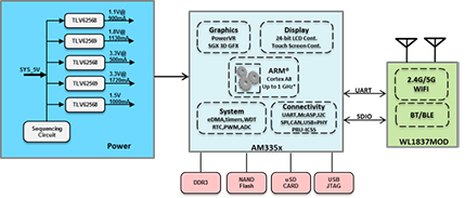
The 12-mm-by-12-mm, 5-Rail Power Sequencing for Application Processors Reference Design, featuring the AM3358 Arm® Cortex® microcontroller, is an example of such an approach (Figure 2). As the title indicates, the total power solution size for the reference design’s five rails, including all required external components like inductors, capacitors and resistors, is just 12 mm by 12 mm.

Figure 2: 12-mm-by-12-mm five-rail power sequencing reference design using SOT563 buck converters

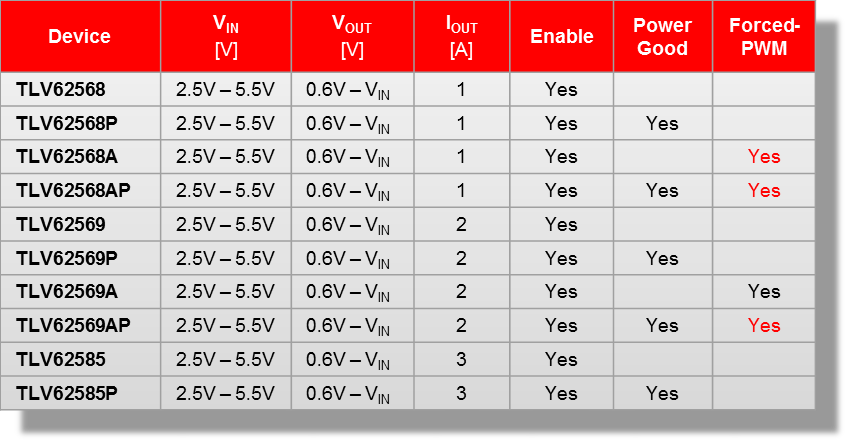
The power consumption of PLC modules is relatively low, typically not exceeding 2 W per module; most power-supply rails are therefore only up to 1 A, 2 A or 3 A. However, thermal constraints often prevent the use of linear regulators and therefore require a high-efficiency DC/DC converter for the point of load, like the new pin-compatible TLV62568/TLV62569/TLV62585 family (Table 1).

 Table 1: TI DC/DC converters available in the SOT563 package

The SOT563 package for DC/DC converters offers many advantages in terms of solution size and ease of use. It is quickly becoming the new standard package for many industrial applications, including those with HMIs and PLCs.

Additional resources

Read these blog posts:

Download the Small Efficient Flexible Power Supply Reference Design for NXP iMX7 Series Application Processors.

Learn more about power management for FPGAs and processors.

Watch the video, “How to meet an FPGA’s DC voltage accuracy and AC load transient specification.

The problem with short-to-VBUS protection integrated into your USB Type-C™/USB Power Delivery controller

$
0
0

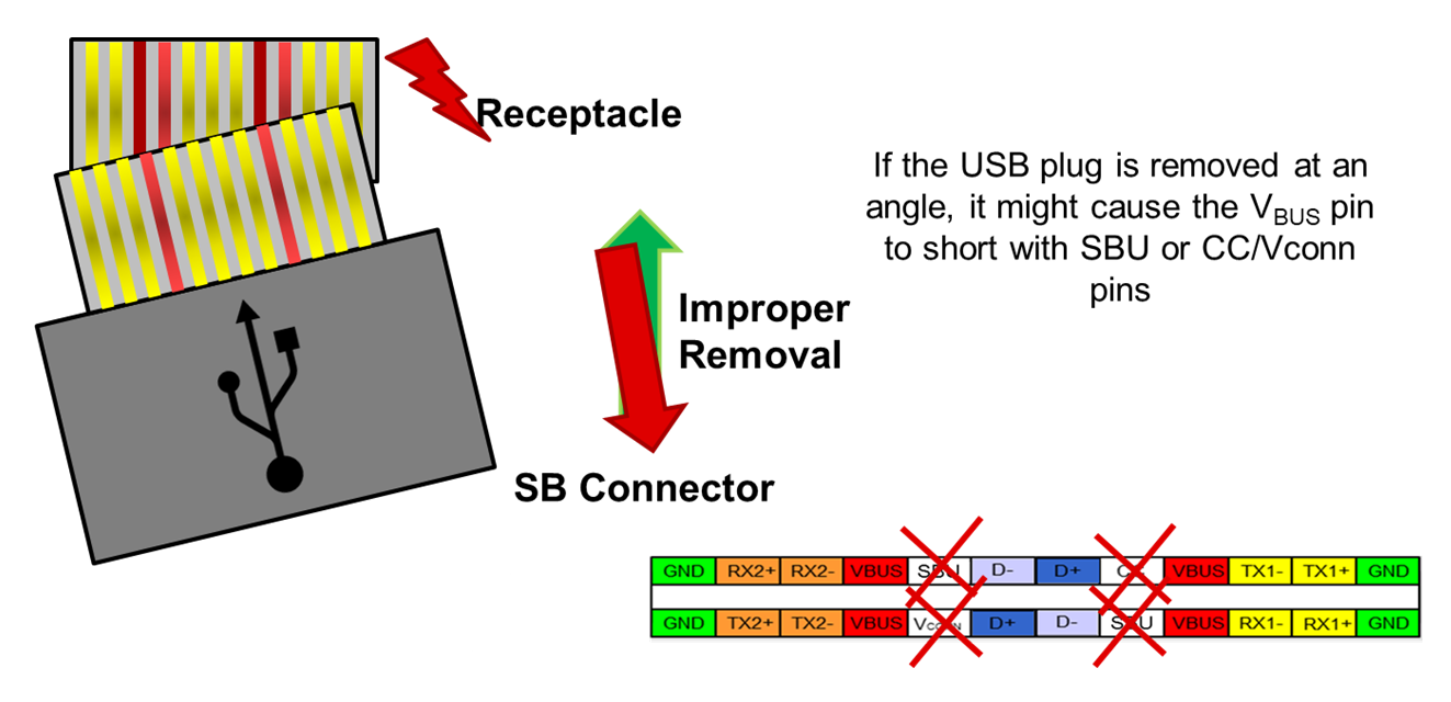
Due to the smaller connector/receptacle size and reduced pin pitch, USB Type-C presents several new failure scenarios that can damage downstream circuitry. The most common failure scenario is mechanical twist; see Figure 1. Once a USB PD contract >5 V (such as 20 V, 15 V or 9 V) has been received by the USB PD Controller, if the USB plug is removed at an angle, it might causethe USB Type-C connector’s bus power lines (VBUS) to short with the adjacent pins – or more specifically the configuration channel (CC) and sideband use (SBU) lines.

Figure 1: Mechanical twist failure scenario

Why does this matter? Well, for most systems, the downstream circuitry (or USB Type-C/USB PD controller) is rated for only 6 V maximum on the CC/SBU pins. Engineers have two choices: add an external protection chip or select a USB Type-C/USB PD Controller with CC/SBU lines rated for 24 V or more. Let’s look into why forgoing the protection chip may not be the best idea.

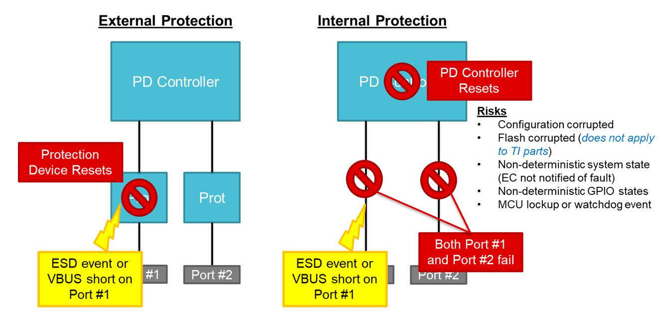
External protection works because if there’s an electrostatic discharge (ESD) event or VBUS shorting on port No. 1, the protection chip opens series field-effect transistors – thus isolating the high voltage from the rest of the system. The chip also dissipates any residual energy (on both system and connector sides) through internal clamping diodes. Then, the protection device resets and protects the rest of the system.
Internal protection doesn’t work because in the case of an ESD event or VBUS short on Port No. 1, the USB PD controller resets itself, bringing down both port No. 1 and port No. 2 as seen in Figure 2. In addition, the USB PD controller runs the risk of having the configuration or flash corrupted during this high rate of voltage change (dv/dt) event. It could leave the system in a nondeterministic state with unknown general-purpose input/output values or even cause the microcontroller to lock up. Even worse, if the USB PD controller doesn’t have properly designed internal clamps to absorb the energy, the device itself could be damaged.

Figure 2: External protection offers fault isolation

These failures are easily avoidable by adding an external protection device such as the TPD6S300A. The TPD6S300A’s ability to clamp the voltage quickly and efficiently helps enable a robust and reliable solution for designers.

Additional resources

How to prevent battery over discharge by using a precise threshold voltage enable pin

$
0
0

Using a buck-boost converter is a convenient way to obtain a fixed supply voltage within the wide voltage range of typical batteries used in low-power devices such as smart meters, wearables or those in the Internet of Things. In order to extract as much energy as possible from the battery, it helps if the converter can operate at very low input voltages.

In buck-boost devices such as the TPS63802, the minimum operating input voltage is as low as 1.3 V once the device is started. With most rechargeable batteries, however, deep discharge can irreversibly damage the battery. In such situations, it becomes useful to have the option to cut off the battery supply at a desired value, say 2.5 V for a one-cell lithium-ion battery.

A typical DC/DC converter has an input pin to enable or disable the converter. However, the threshold voltage at this pin usually has a high tolerance, making it difficult to pinpoint the desired cutoff voltage. As an example, according to its data sheet, the threshold voltage of the enable (EN) pin for the TPS63020 is somewhere within the range listed in Table 1. 

Parameter

Min

Typ

Max

Unit

VIL

EN input low voltage


0.4

V

VIH

EN input high voltage

1.2


V

Table 1: EN pin threshold voltage for the TPS63020

This threshold range is fine for on/off control using logic-level signals, but not if you want to set a precise cutoff voltage derived from the input voltage. To achieve higher accuracy, it is possible to add a comparator and a voltage reference, but this increases complexity and cost.

My colleague Chris Glaser introduced the concept of achieving a precise threshold voltage for buck converters in his Analog Design Journal article, “Achieving a clean startup by using a DC/DC converter with a precise enable-pin threshold.” The new TPS63802 buck-boost converter also has very precise threshold voltage for the EN pin, with approximately 3% accuracy and 100-mV hysteresis, as listed in Table 2. 

Parameter

Min

Typ

Max

Unit

VTHR,EN

Rising threshold voltage for EN pin

1.07

1.1

1.13

V

VTHF,EN

Falling threshold voltage for EN pin

0.97

1

1.03

V

Table 2: EN pin threshold voltage for the TPS63802

It is possible to easily set a user-defined minimum supply voltage with a voltage divider, as shown in Figure 1.

 Figure 1: Setting the input cutoff voltage with a voltage divider

Equation 1 expresses the falling threshold supply voltage when the converter is turned off as:


Equation 2 calculates the rising threshold supply voltage when the converter is turned on:


The additional voltage divider will increase the current consumption; therefore, aim for large resistances. However, considering that the EN input leakage current is 0.2 μA maximum, aim for at least 20 μA of current in the voltage divider. The application report, “Optimizing Resistor Dividers at a Comparator Input,” has more details about how to optimize a resistor divider at a comparator input.

As an example, to set the cutoff input voltage to VTHF,IN = 2.5 V, first choose R1 + R2 = 125 kΩ to have a 20-μA resistor divider current. Solving Equation 1, choose R1 = 75 kΩ and R2 = 49.9 kΩ resistors with 1% tolerance. The turn-on input voltage is now VTHF,IN = 2.75 V according to Equation 2.

Figure 2 shows that the achieved cutoff and turn-on input voltages are 2.56 V and 2.8 V, respectively. This is within the equivalent 6σ tolerance of approximately 80 mV (3.1%) caused by the EN pin threshold voltage and resistor tolerances, not taking into account oscilloscope accuracy. The application report, “AN-1378 Method for Calculating Output Voltage Tolerances in Adjustable Regulators,” has more details on calculating equivalent voltage tolerances.

Figure 2: Achieved cutoff and turn-on input voltage thresholds

Conclusion

The previous example showed how you can easily protect your battery from overdischarge by adding only 2 resistors. The same solution is applicable not only to buck-boost but also to other buck or boost devices with a precise EN pin threshold voltage.

If you have any questions about TI buck-boost devices, see the TI E2E™ Community Power Management forum.

Output topology options for a voltage supervisor

$
0
0

 Having stumbled upon this blog post, I’m assuming that you know the importance of having a voltage supervisor in your electronic design and are wondering how to implement and design with these different output topology types. Don’t worry! You came to the right post. But before I explain the different output topologies, I want to reiterate the importance of having a voltage supervisor, as many engineers are not familiar with this device.

Given the variable amounts of load that a system can have, the power supply is not always clean and can bounce around its typical output value. With this bounce in power supply, a device known as a voltage supervisor can provide protection from accidental surges or falling power, and improve the efficiency of electronic devices. This makes voltage supervisors a requirement in any electronic application.

The voltage supervisor products available on the market distinguish themselves by features such as threshold selections, multichannel monitoring options, detection accuracy, output configurations, fixed or adjustable delay, and watchdog features. In this post, I’ll focus on the different output configurations and review what you should consider when designing with these output topologies.

Output configurations

Think of a supervisor as an analog-to-digital converter. It senses a supply voltage (analog) and provides a flag (either the RESET or SENSEOUT pin), which is a digital signal. The digital signal output can be in either an open-drain or push-pull topology.

The open-drain output topology

Here are some things to consider when designing with the open-drain output topology:

  • Open-drain outputs provide flexibility because they can pull up to any voltage (within absolute maximum) to comply with the logic of the load, rather than pulling the output up to the supervisor’s supply voltage or sense voltage. A pull-up resistor properly limits the current and maintains the low-level output voltage (VOL) and high-level output voltage (VOH) specifications.

  • It’s possible to wire-OR together multiple open-drain outputs through a single pull-up resistor. The open-drain output can also pull up to any voltage that complies with the logic of the load giving flexibility to a designer.

  • The pull-up resistance cannot be too low such that the current through the open drain damages the supervisor. When the internal n-channel metal-oxide semiconductor (NMOS) (Figure 1) is on, current from the pull-up resistor will go through the NMOS and be pulled to ground. You should select the pull-up resistance based on two criteria. The first criteria is the supervisor’s recommended maximum reset or sense current, called IRESET or ISENSE, which is specified in the data sheet. If the current being pulled to ground is higher than IRESET, the supervisor’s internal NMOS could be damaged. The second criteria is based on the VOL requirements of the load that the output of the voltage supervisor connects to. Lower pull-up resistors will also result in higher VOL due to the increase in reset/sense current.

  • The pull-up resistance cannot be too high such that the leakage current through the open-drain resistor at high temperatures falls outside the VOHspecification found in the data sheet. By increasing the pull-up resistance, VOH decreases due to the smaller reset or sense current, causing a smaller voltage drop across the internal metal-oxide semiconductor field-effect transistor (MOSFET).

  • The output rise time is decided by the pull-up resistance and the output board parasitic capacitance. For faster rise times, use smaller pull-up resistances.

  • The supervisor’s quiescent current (Iq) does not include the current through the pull-up resistor. If the pull-up voltage is pulled from the supply, the total system Iq will increase, as supply current will also go through the pull-up resistor. If the pull-up voltage connects to another source, the system Iq will equal the supervisor Iq from the data sheet. Since the pull-up voltage can connect to different supplies, the Iq specification of the supervisor does not account for the additional output current resulting from the use of a common supply.

  • An open-drain output configuration requires an additional component, a pull-up resistor, connected from the output to a power supply. Without the pull-up resistor, the outputs are undefined when the internal NMOS turns off, as there will be no power supply to pull from.

  • The open-drain output can change with the output pull-up supply, and any transient coupling will depend on the pull-up resistance used. A higher pull-up resistance can minimize the effects of transients from the output pull-up supply.

Figure 1: The open-drain output uses an internal N-MOSFET

The push-pull topology

Here are some things to consider when designing with the push-pull output topology:

  • The output of a push-pull configuration toggles between the supervisor’s supply voltage and ground, with no external pull-up resistance required. Notice how the output in Figure 2 does not use a resistor like in Figure 1, and how Vpullup is not present in Figure 2. Vdd and ground are toggled via the 2 MOSFETS.

  • The voltage at the output of a push-pull configuration can never go beyond the supervisor’s voltage supply by more than 0.3V, because the body diodes can turn on and damage the device. The body diode will take excessive current in forward bias mode.

  • The quiescent current of the supervisor accounts for the current through the external resistors that can be connected at the output of the supervisor.

  • It’s not possible to wire-OR together push-pull outputs like with the open-drain output topology.

  • Push-pull outputs are a good fit for high-speed applications because the push-pull output does not have the additional delay that the pull-up resistor causes in the open-drain topology.

Figure 2: In the push-pull output topology, a p-channel MOS (PMOS) and NMOS connect together, similar to an inverter

How to identify active low and active high

Different types of supervisors monitor under and overvoltage conditions and provide RESET/FLAG/POWERGOOD/SENSEOUT in an active-low or active-high output topology. “SENSEOUT” and “POWERGOOD” labeled pins are active when the supervisor senses the supply voltage is in normal operating condition, whereas a “RESET” labeled pin is active when the supervisor senses the supply voltage is in a fault (under- or overvoltage) condition.

An overvoltage active-high supervisor means that whenever the supply crosses VIT+, signaling an overvoltage condition, RESET activates to logic high.

Table 1 can help you identify the different supervisors.

Table 1: Active-high vs. Active-low supervisors.

Now that you know more about the different output topologies, you are one step closer to selecting the correct supervisor for your system. Check out TI’s quick search tool to help you find one.
Additional resources

What does a “lead-free” power MOSFET really mean?

$
0
0

Much confusion exists today with the term “lead-free.” What does it mean? Why is it important? How can you tell if a component or product is lead-free?

A web search of the term produces many hits, including lead-free gasoline, plumbing, jewelry, glass and yes, lead-free electronics. The purpose of this blog post is to clarify what lead-free means and how TI metal-oxide semiconductor field-effect transistor (MOSFET) products comply with lead-free requirements.

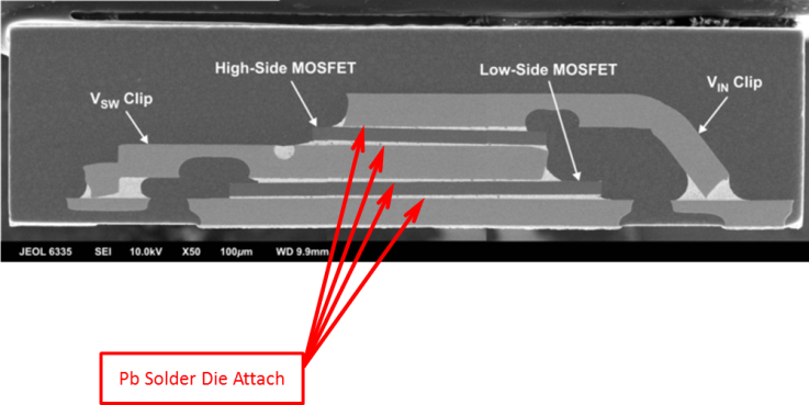
Let’s start with a brief history of lead content in electronic components and assemblies. For many years, manufacturers used tin-lead solder to attach components to printed circuit boards. Similarly, lead-containing solder is used in the assembly of components like power MOSFETs and multichip modules to attach silicon die to copper leadframes and packages. Eliminating lead is the goal of all MOSFET vendors, but as of today, a leaded solder die attached still provides the best electrical and most reliable and cost-effective solution.

Lead-free compliance requirements

Lead is a known hazardous material that can cause detrimental health effects. Growing concern over the disposal of electronics, called e-waste, led to the adoption of the European Union’s (EU) Restriction of Hazardous Substances (RoHS) Directive 2002/95/EC (RoHS 1) in February 2003. RoHS 1, which became effective in July 2006, restricted the use of six hazardous substances, including lead, in the assembly of electronic and electrical equipment. RoHS 2 expanded the list of banned substances and took effect in January 2013.

There are a number of exemptions to RoHS directives, however. A small number of these exemptions are applicable to TI integrated circuits:

  • Exemption 7(a): lead in high-melting-temperature-type solders (lead-based alloys containing 85% by weight or more lead).
  • Exemption 7(c)-I: electrical and electronic components containing lead in glass or ceramics other than dielectric ceramic in capacitors (such as piezoelectric devices), or in a glass or ceramic matrix compound.

  • Exemption 7(c)-IV: lead in lead zirconate titanate-based dielectric ceramic materials for capacitors that are part of integrated circuits or discrete semiconductors.

  • Exemption 15: lead in solders to complete a viable electrical connection between semiconductor die and carriers within integrated circuit flip-chip packages.

All TI FET devices are lead-free external to the package. Many TI MOSFET products use leaded solder for die attachment to a leadframe and/or copper clip and are subject to Exemption 7(a). Figure 1 shows the stackup of a TI power block (a dual MOSFET device).

Figure 1: Cross Section of TI Power Block

Unfortunately, there is general lack of industry standards for documenting the lead-free status of semiconductor devices. The available information can be misleading and the designer may not know if the device they have selected is 100% lead-free. The onus is on the designer to check the bill of materials for every device selected.

Where to go for lead-free status of TI MOSFET products

When reviewing compliance for a specific TI device number, there are several places to find RoHS information.

  • Start with the data sheet. TI will include the term “RoHS compliant” in the Features bullet list on the first page of a TI data sheet. In better to understand the device compliance, you should also review the Eco Plan in the Packaging Information section near the end of the data sheet. In that section, TI uses this terminology:

  • RoHS” means semiconductor products that are compliant with current EU RoHS requirements for all 10 RoHS substances, including the requirement that an RoHS substance not exceed 0.1% by weight in homogeneous materials. Where designed to be soldered at high temperatures, RoHS products are suitable for use in specified lead-free processes. TI may reference these types of products as “Pb-Free.”

  • RoHS exempt” means products that contain lead but are compliant with the EU RoHS pursuant to a specific EU RoHS exemption.

  • Green” means that the content of chlorine- and bromine-based flame retardants meets Joint Electron Device Engineering Council JS709C low halogen requirements at a ≤1,000-ppm threshold. Antimony trioxide-based flame retardants must also meet the ≤1,000-ppm threshold requirement.

  • Material content search on TI.com. If you need additional details, you can use the material content search function on TI.com for a specific device number.

 Table 1 shown below summarizes the lead free status of TI discrete MOSFET and power block products.

Product category = single MOSFET

Package description

Package suffix

100% lead-free

RoHS exempt

Land grid array (LGA)

F3, F4, F5, L

Y

N

Wafer-level packaging (WLP)

W, W10, W15, W1015

Y

N

2-mm-by-2-mm small outline no-lead (SON)

Q2

Y

N

3-mm-by-3-mm SON

Q3A

Y

N

3-mm-by-3-mm SON

Q3

N

Y

5-mm-by-6-mm SON

Q5, Q5A, Q5B

N

Y

Transistor outline (TO)-220

KCS

N

Y

D2PAK

KTT

N

Y

Product category = dual MOSFET

Package description

Package suffix

100% lead-free

RoHS exempt

LGA

L

Y

N

WLP

W15, W1015, W1723

Y

N

S0-8

ND

Y

N

2-mm-by-2-mm SON

Q2

Y

N

3-mm-by-3-mm SON

Q3

N

Y

3-mm-by-3-mm SON

DMS

N

Y

Product category = power block

Package description

Package suffix

100% lead-free

RoHS exempt

3-mm-by-3-mm SON

Q3D

N

Y

5-mm-by-6-mm SON

Q5D

N

Y

5-mm-by-6-mm dual-cool SON

Q5DC

N

Y

PB II

P, N, M

Y

N

Table 1: TI discrete MOSFET and power block lead-free status

Conclusion

TI strives for compliance with all regulations regarding the use of lead in its MOSFET products. Not all lead-free devices are created equally. Many power MOSFET products from TI and other vendors are lead-free external to the package but use leaded solder internally for die attachment and interconnect. Always check the material content for a device from TI to determine whether it is RoHS compliant and if there are any exemptions.

Additional resources

Searching for the newest innovations in power? Find them at APEC

$
0
0

The Applied Power Electronics Conference (APEC) is a power engineer’s dream – everyone in the industry attends and the blend of new technologies, new research and new connections creates an electric energy. Last year, APEC had over 5,000 attendees making it one of the largest power conferences in the world. TI is proud to be a part of it – we’re hosting five industry sessions, four poster sessions and three technical lectures; we’re excited to share the experience with you!

Here is all you need to know about TI’s involvement in the 2019 APEC conference, this blog will include everything required to plan your upcoming days at the conference and will be updated in real time with new content. Even if you can’t make it to APEC this year, be sure to check back for live updates!

Attending APEC?Join us at booth #511 and at our technical presentations (PDF) this year!


Demos you’ll find at our booth:

  • More power, less space

    • Faster charging with USB Type-C™ technology: Learn how to experience faster charging with USB Type-C™ technology for both AC/DC and automotive applications using gallium nitride and silicon. See how our award-winning UCC28780 active clamp flyback controller enables industry-leading power density for AC/DC adapters.
    • Digitally controlled adaptive peak current mode-controlled phase-shifted full bridge for onboard charging: This demo showcases a new reference design that leverages the differentiated on-chip control and protection features on the C2000™ F280049 microcontroller to enable adaptive peak current mode control of a phase-shifted full-bridge converter without the need for external hardware support circuitry.
    • 330-W, high efficiency at low line input, gaming notebook adapter: Improve the power density of your AC/DC 330-W gaming notebook adapter with this reference design. The design’s efficiency is higher than 95% at full load, while the power density is higher than 18 W/in3, with natural cooling and power consumption lower than 0.5 W at no load. In order to reach this level of efficiency, the design uses advanced bridgeless power factor correction and a soft-switching inductor-inductor-capacitor topology.
    • Digitally controlled high-voltage, power, efficiency and density bidirectional chargers with SiC FETs: A new 6.6-kW bidirectional CLLLC DAB isolated DC/DC reference design with 300- to 700-kHz switching features the C2000™ F280049 microcontroller and UCC21530-Q1 silicon carbide gate drivers. This design highlights advanced digital control techniques and wide band-gap technology to enable higher efficiency and higher density chargers. Pairing with the totem-pole PFC reference design provides a complete solution for high-voltage battery-charging applications for onboard chargers (conventional and vehicle-to-grid) and grid storage.

  • Extending battery life 

    • Three functions in a single-chip solution: This demo features the BQ40Z80 battery pack manager as we demonstrate how it monitors and protects a battery pack cell by cell while using our patented Impedance Track™ technology for accurate gauging. Designed with ease of use in mind, this device enables eight multifunction pins for configurability in a single chip.
    • Accurate gauging and 50-μA standby current, 13S, 48-V Li-ion battery pack reference design: Optimize your e-bike 13S battery pack system design with extended run time and idle time and low current consumption with our accurate gauging reference design. This design features state-of-charge gauging based on the BQ34z100-G1 and this demo will show the two ways to improve energy utilization efficiency by increasing state-of-charge accuracy and reducing current consumption.

Where else can I find TI?

  • Learn by doing: Get a head start on solving your toughest application challenges
    • Join TI and Würth Elektronik for hands-on experimentation with the new TI-PMLK Buck Würth Elektronik edition. This new power management laboratory kit (PMLK) includes two distinct buck circuits with different operating conditions, six different inductors for testing, adjustable operating conditions, protection features and a temperature probe. Würth Elektronik’s demo will include a full instrumentation setup, as well as the TI-PMLK’s complete experiment book, so you can get a head start on investigating conditions that impact real-world applications.

  • +240-W dual-output step-down PMBus power module powering an FPGA core and I/O rails
    • See the world’s first dual-output PMBus module, capable of >200 W of output power with tight load regulation. The TPSM831D31EVM evaluation module (EVM) is configured to evaluate the operation of the TPSM831D31 power module and has the industry’s highest-current multiphase PMBus power module for two high-current step-down rails. This EVM provides high power density, efficiency, design programmability and system monitoring through PMBus in 720 mm2 of printed circuit board area, perfect for high-current field-programmable gate array and application-specific integrated circuit cores and input/output rail applications.


Design a pre-tracking regulator, part 1: for a positive-output LDO

$
0
0

By Arief Hernadi and Frank DeStasi


The efficiency of a low-dropout regulator (LDO) depends on its input voltage and output voltage, since the input current drawn from the power supply will be equal to the current required at the output of the LDO. Therefore, a higher input and output voltage difference in the LDO translates to a lower efficiency value, and vice versa. An LDO with low efficiency translates into power loss and causes heating inside the device.


Sometimes, you are going to need an LDO at the point of load because of its low-noise properties. For example, in an automotive rear camera design, an LDO can provide power to the analog circuitry of the Flat Panel Display (FPD)-Link serializer, which normally requires a 1.8-V rail. As the input voltage rail normally starts from a battery (12 V or 24 V), one way to increase the overall system efficiency is to use a DC/DC converter as the first stage of conversion, followed by an LDO.


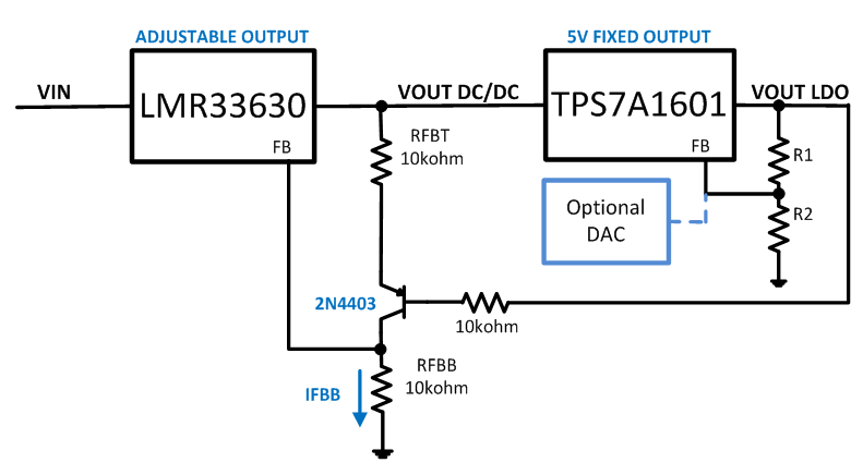
Since LDO efficiency depends on the difference between its output and input voltage, another way to increase overall system efficiency is to use a tracking pre-regulator circuit, as shown in Figure 1. In this case, the VOUT of the DC/DC will always be regulated into a fixed amount above the VOUT of the LDO. The circuit in Figure 1 gives you flexibility to dynamically adjust the LDO voltage without adjusting the voltage on the DC/DC converter individually.


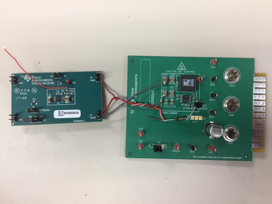
The pre-regulator circuit shown in Figure 1uses TI’s LMR33630 synchronous buck converter and TPS7A1601 LDO evaluation modules (EVMs), with some modifications to the LMR33630 feedback network. The LDO chosen here is a 60-V LDO, but you could also use a lower-voltage LDO such as the TPS7A4701.

Figure 1: A positive-tracking pre-regulator with the LMR33630 and TPS7A1601

In Figure 1, the feedback from the LMR33630 generates a constant current, IFBB, which flows through the feedback network, RFBT and RFBB.

Figure 2: Hardware implementation

In this configuration, the VOUT of the DC/DC will follow the VOUT of the LDO according to Equation 1:


In order to adjust the headroom of the LDO, simply adjust the value of RFBT: IFBB will remain constant.


In the sample design of Figure 1, the TPS7A1601 EVM is set to generate a 5-V output; the LDO output voltage connects to the base of the 2N4403 P-channel N-channel P-channel (PNP) transistor with a 10-kΩ resistor. Since the LMR33630 internal reference voltage is 1 V, the voltage at the VFB of the LMR33630 is also regulated at 1 V.


Following Equation 1, the value of IFBB = 1 V/10 kΩ = 0.1 mA. The Vbe of the 2N4403 is approximately 0.6 V:

 In general, the LMR33630 output voltage will be about 1.6-V higher than the LDO output voltage; this is the LDO headroom.


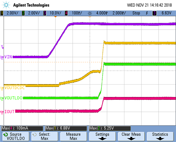
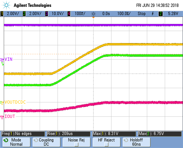
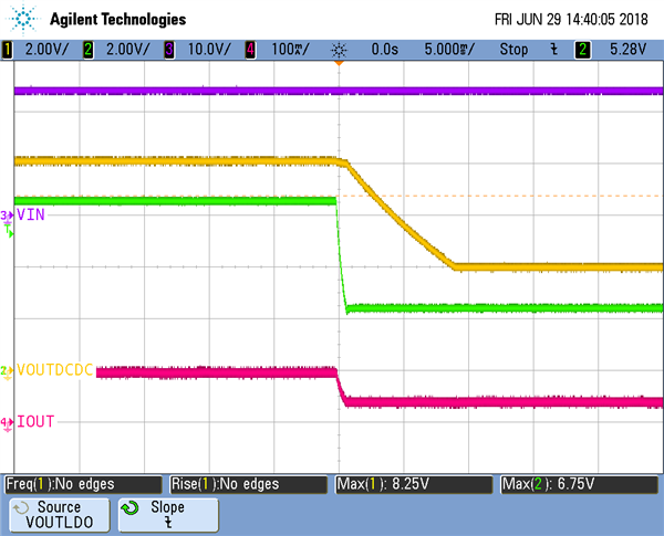
The waveforms in Figures 3 and 4 illustrate the performance of the system.
 

Figure 3: Startup waveform, with the LMR33630 tracking the LDO voltage

Figure 4: The LMR33630 tracking the up-ramp of LDO voltage (the LDO feedback network is injected with a ramp to control its output voltage)


As you can see in Figure 4, the TPS7A1601 voltage rmps up with a rise time of 200 µs and the LMR33630 output voltage tracks quite nicely, at 1.6 V above the LDO voltage. Since there is less output current on the LDO, this means that there is only a small load on the LMR33630. Therefore, during the down transition, the LDO voltage ramped down faster than the LMR33630 output voltage (note the time base shown in Figure 5). Once both voltages settle, you can see in Figure 5 that the LMR33630 output voltage is still above the LDO voltage by 1.6 V.


Figure 5: The LMR33630 tracking the down-ramp of the LDO voltage


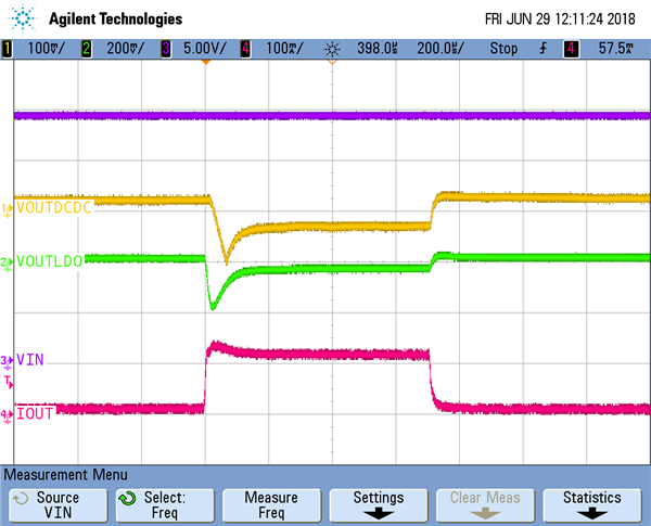
One last thing to check is the overall system stability by performing load-transient testing at the output of the TPS7A1601 LDO. Figure 6 is a scope capture showing a load transient at the output of the TPS7A1601 LDO from 0 to 100 mA. The scope shot shows that even during a load transient, the LMR33630 tracks the TPS7A1601 LDO output voltage.

Figure 6: Load-transient waveform for the TPS7A1601 from 0 to 100 mA (VOUTDCDC and VOUTLDO are AC-coupled)


As you can see, it is possible to employ a tracking pre-regulator to increase the overall system efficiency of an LDO with a DC/DC converter by minimizing the difference between the input and output voltage of the LDO. In part two of this series, we’ll use a similar technique to create a tracking pre-regulator for a negative output LDO.

Pull the tab: How to implement ship mode in your lithium-ion battery design

$
0
0

Remember when you were a kid, and many of your battery-operated toys had a little plastic pull tab on the battery (Figure 1) that you pulled off to make the product come to life? This closes the connection from battery to the active circuit on the product and is one of the earliest implementations of “ship mode.”

In this blog post, I will address what ship mode is, and how you can use this feature in your product to deliver the best user experience. While I will be using TI battery charge management integrated circuits as examples, you can apply these concepts to any low-power system under development.

  
Figure 1: Pull tab on a battery-operated product

What is ship mode, and why do you need it?

Ship mode is the state in which the product is consuming the lowest battery current. Consumers naturally want to use battery-operated products immediately after purchasing them. This means that the battery has to maintain some capacity during transportation from the factory and during its shelf life, which could be a couple of months or even longer. 

Lithium-ion batteries have become a popular choice for designers because they are rechargeable, support high-power requirements and are very light. However, unlike non-rechargeable batteries, you can’t put plastic tabs on products using lithium-ion batteries as you want to restrict access to these batteries for safety concerns. This means that we need to find alternative solutions for implementing the ship-mode feature for products both in its on and off states.

You might be wondering why you should care about ship mode when “shipping” happens only once, but that’s not exactly true. Ship mode is the state in which the product is consuming the lowest quiescent current, while waiting for the user to press a button to turn the product ON. For instance, TI’s BQ25120A is actively monitoring for either an adapter to be plugged in or a button-press input, all while consuming a typical current of 2 nA.

I often recommend that designers implement ship mode when the product is about to be boxed at the factory, is being used and running low on battery, and is being used and the user wants to power off the product.

The ship mode on the BQ25120A family of chargers is realized using a push-button interface, as shown in Figure 2. The push-button input (/MR) is internally pulled up to the VBAT pin. When the device is in ship mode and the user presses the /MR button, the product comes out of ship mode.

You don’t need a capacitor on this pin, as the signal is internally deglitched, but it is common to see them on some schematics. You could optionally use a transient voltage suppression diode for protection if the switch is exposed to the user. A low-voltage read on the /MR pin translates to a “button pushed” action. Take care when connecting to a microcontroller (MCU) to drive the /MR pin, as voltage on the /MR pin is pulled to the battery voltage itself. An N-channel metal-oxide semiconductor is often employedto mimic a “press” action from the MCU in a buttonless system. 


Figure 2: Internal pullup on the /MR pin

When a product is about to be boxed at the factory, the EN_SHIPMODE command is sent over I2C and the device waits to go to ship mode until the VIN(charger) is disconnected, as shown in Figure 3.

 Figure 3: Illustration of ship mode at a factory production line

I have seen many challenges on the production line. Things work great in the lab, but on a line that’s building a few hundred products an hour, it can be a different story. The product is on a jig and the assembler doesn’t have a proper way to pull off the product without the VINadapter bouncing. The charger will get out of ship mode when VINlooks like it was plugged back in. How do you make sure that the product is in ship mode in this case?

The answer is simple: Set the EN_SHIPMODE command when the VINis present. Once the product is off the jig that supplied the VIN, raise the /CD pin high to complete the execution of the ship-mode command and put the device to a ship mode before being boxed, as shown in Figure 4. In all these sequences /MR is being pushed to show that the device has indeed gone into ship mode.

 Figure 4: Illustration of ship mode at a factory with a bouncy adapter

When the product is running low on battery, often the best way to power down is to keep some reserve capacity and then go into ship mode. When the user presses the button, the device can read the battery level. If the battery level is too low, the product can display a warning and return back to ship mode, as shown in Figure 5. When using the BQ25120A, for example, you can send the ship-mode command using a single register write as shown in Figure 6.


Figure 5: Wake-up routine for your product

 Figure 6: Ship mode entry through I2C command

Also, to create a power on/off button, you could still use the /MR pin by configuring the MRREC register to go to ship mode and programming the duration of the button of how long it needs to be held low; you’ve just created yourself a power-off button. To wake back up, press the button again, as illustrated in Figure 7.

 Figure 7: Power on/off button

I hope that this post has given you a good idea on how to use some of the features that are present on a charger and ready to implement ship mode in your next product! Visit our E2E forums for any questions you might have. 

Additional resources


Four-switch buck-boost layout tip No. 4: routing gate-drive and return paths

$
0
0

Printed circuit board (PCB) layout design plays a critical role in achieving high performance for a four-switch buck-boost regulator. In earlier installments of this series, we discussed strategies for placing the regulator’s power components, AC current loop design and current-sense trace routing. In this installment, I will focus on optimal routing of the gate-drive and return paths.

The gate-drive signal for each of the four metal-oxide semiconductor field-effect transistors (MOSFETs) runs along a closed loop. Figure 1 shows the LM34936 or LM5176 four-switch buck-boost controller as an example.

Figure 1: Gate-drive and return path routes

In a real circuit, PCB traces usually have parasitic resistance, inductance and capacitance. The PCB trace capacitance for the gate drive is normally negligible, so I will ignore it here. Figure 2 shows the equivalent gate-drive circuit. RTrace1 is the PCB drive trace resistance, RTrace1 is the drive return trace resistance, LTrace1 is the drive trace stray inductance, LTrace2 is the return path inductance and Ciss is the MOSFET gate input capacitance. The trace resistance and inductances can cause gate signal delays; therefore, it’s best to keep the drive and return traces as short as possible.

Figure 2: Gate-drive equivalent circuit

Given board area limitations, it is not possible to place the driver very close to the MOSFET. Even if the MOSFET is not very close, it is possible to make RTrace1 and RTrace2<1 Ω in most designs. LTrace1 and LTrace2 can become significant if the trace routing is poor, however. An inductance of just a few nanohenries may resonate wildly with the MOSFET gate capacitance and create gate voltage ringing, as shown in Figure 3. If the magnitude of the ringing exceeds the MOSFET gate threshold voltage, Vth, it will cause unwanted extra switching action and result in severe switching losses inside the MOSFETs.

Figure 3: Gate ringing and unwanted extra switching action

So how can you minimize the gate-drive inductance? According to physics, the gate-drive inductance is proportional to the spatial area enclosed by the drive current loop, which is the area defined by the actual drive and return traces. Minimizing the spatial area of the drive current loop should be your main focus in routing the MOSFET drive and return paths.

Assume that the drive is at point A and the MOSFET is at point B on the PCB; the drive trace must be routed from point A to point B and return back to point A. Also assume that a straight trace from A to B is not possible because other components are in the way. Figure 4 shows two different routing patterns. Obviously, option No. 2 encloses a minimal spatial area and thus produces the least inductance, even though the total trace length is the same as option No. 1. This example clearly shows that the optimal routing is to place the drive and return traces closely side by side for the entire distance between the driver and the MOSFET.

Figure 4: Routing patterns for current loop traces between points A and B on the PCB


Again, given board area limitations, sometimes there is no space to place the pair of drive and return traces side by side on the same layer. A solution is to route the return trace in the shadow of the drive trace on an adjacent layer, as shown in Figure 5, where the drive trace runs from point A (Drive) on Layer 1 to point B (MOSFET), and takes the via hole to Layer 2, and runs back to point A in the shadow of the drive trace. In this way, the drive and return traces basically run closely side by side in the vertical direction, minimizing the spatial area enclosed by the signal loop.

Figure 5: Routing the return trace in the shadow of the drive trace on an adjacent layer to minimize loop inductance

You should apply these schemes, either running side by side or overshadowing, when routing the two high-side MOSFET drive traces, namely the HDRV1/SW1 and HDRV2/SW2 traces. For the two low-side MOSFETs, the two drive return paths run back to the PGND pin. If the PCB has multiple layers that include a ground plane layer, then you just need to route the LDRV1 and LDRV2 traces and let the return path take the ground plane. Because current naturally takes the path with the least impedance, the return path will be virtually in the shadow of the LDRV1 or LDRV2 traces, as depicted in Figure 5.

If the ground layer is not available, then you can route both the drive and return traces side by side on the same layer. There should be two dedicated pairs of traces: one pair of LDRV1/PGND traces and one pair of LDRV2/PGND traces for the two low-side MOSFETs.

Conclusion

In order to optimize four-switch buck-boost performance, keep the gate-drive traces as short as possible. If the PCB space does not allow you to place the MOSFET very close to the drivers, then route the gate-drive signal such that the pair of drive and return traces are placed closely side by side – either on the same PCB layer or on adjacent layers – to minimize the spatial area enclosed by the drive signal loop. Doing this minimizes the parasitic inductance, prevents gate-drive ringing, minimizes switching losses and achieves high performance for a four-switch buck-boost converter.

Additional resources

  • See the LM34936 or LM5176 data sheets for detailed layout guidelines and the LM34936 and LM5176 evaluation modules for layout examples.

20 million GaN reliability hours and counting

$
0
0

"My advice is to get involved and get started,” — Jack Kilby

About 20 million reliability hours ago, we built our first gallium nitride (GaN) application board in TI’s Kilby Labs. We watched the oscilloscope in anticipation and were amazed at the textbook-like switching waveforms. Power GaN was at an early stage of technology maturity but showed tremendous promise. Integrating a driver and protection features would indeed make the perfect power switch. We knew there was lot of work ahead, so we took Jack Kilby’s advice.

Our early evaluation marked the start of a reliability journey, as we realized that traditional silicon qualification was not testing for hard switching. Many power-management applications hard-switch the field-effect transistor (FET), making this finding very relevant. Hard-switched circuits include buck and boost converters, power factor correction circuitry, inverters and motor drives. Hard-switching stresses the device in a different way, since it includes a brief moment where the device is subject to simultaneous high voltage and current as described in our white paper, “A comprehensive methodology to qualify the reliability of GaN products.”

We realized that the devices needed to be made robust to hard-switching. The methodology in use for silicon was not applicable to GaN, so we started hard-switching the FETs in a boost-converter test vehicle as part of our device development program. This issue of application robustness quickly became known in the industry, along with the need to collaborate, as described in our blog post, “Let’s GaN together, reliably.”These aspects catalyzed the formation of the Joint Electron Device Engineering Council (JEDEC) JC70 committee on wide bandgap power electronic conversion semiconductors, and have accelerated the availability of reliable GaN.

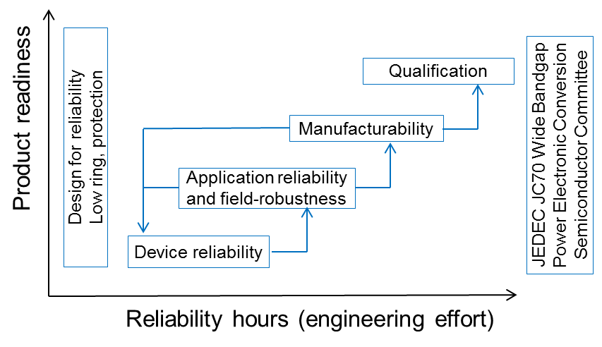
Reliability is our highest priority, and we knew that the release of a reliable technology to manufacturing encompasses much more than hard switching, as illustrated in Figure 1. The LMG341x family of devices has both reliable GaN and silicon, is manufacturable, incorporates protection features, is integrated into a low-inductance package, and is validated to work robustly in applications. These device features were achieved with coordinated efforts in device reliability, application robustness and manufacturability, in addition to considerable accelerated stress testing and failure analysis.

Figure 1: A methodical path to the manufacture of high-quality dependable products. In addition to substantial reliability effort in device engineering, application robustness and manufacturability programs, the LMG341x device also has design-for-reliability features and benefits from our participation on the JEDEC JC70 committee

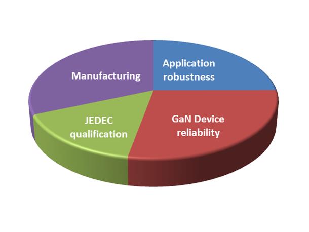
We take successful designs through a standard qualification procedure, involving both GaN-only and LMG3410 devices. Nowhere is Thomas Edison’s quote, “Genius is 1% inspiration and 99% perspiration,” more true, and we have certainly made our devices perspire in hot and humid chambers. We have conducted over 20 million hours of reliability testing, as shown in Figure 2, broken down into four categories: manufacturing, application robustness, GaN device reliability and JEDEC qualification.

Figure 2: Pie chart showing the breakdown of the various categories of reliability testing hours

It’s easy to see how the reliability hours accumulate. GaN device reliability is designed through the understanding of the time-dependent breakdown failure mode, field plate engineering, the judicious choice of appropriate materials and thicknesses, and by engineering the epitaxially grown layers. We run large quantities of regular devices and special test structures specially designed for understanding failure mechanisms, testing 10,000 wafer-level structures and 8,000 packaged devices to build comprehensive reliability models and predict device lifetimes. Our model shows that the overall FET and high-field-withstand components have lifetimes of over 100 years.

We also tested devices for stable dynamic RDS(on) and hard-switching safe operating areas by routinely running them on application reliability test boards for 1,000 hours. Dynamic RDS(on) is a measure of the on-resistance that power-supply designers see during product operation and is a consequence of charge trapping by high fields. Dynamic RDS(on) reliability engineering consists of optimizing interfaces, developing in-process cleans that leave pure surfaces, depositing high-quality dielectrics and optimizing growth parameters of the GaN epitaxial layers. We test the multichip module (MCM) at the system level using our customer evaluation module card to ensure that there are no effects from the interactions of the components or in other modes of operation, such as synchronous rectification. We also test the MCM for extreme conditions like short circuits and lightning surges.

Manufacturability and use of the mature silicon infrastructure also forms a key part of our program. Silicon manufacturing processes are very cost-efficient, not only in wafer processing, but also in the packaging process of wafer thinning, die singulation and assembly. In order to develop good GaN manufacturing, we have run over 10,000 devices in burn-in boards, both for early failure detection and for longer-term high-temperature reverse-bias validation testing. We have also run the well-proven traditional (JEDEC) qualification on both the intrinsic technology and the product, including extending the major tests to 2,000 hours, double the regular stress time.

With 20 million hours of stress testing behind us, there are now many good reasons to find out more about the perfect power switch at http://www.ti.com/GaN.

Replace your aging optocoupler gate driver

$
0
0

Electric motors are used in elevators, food processing equipment, factory automation, robots, cranes … the list goes on. AC induction motors are common in such applications, and invariably, the insulated gate bipolar transistors (IGBTs) used in the power stages to drive them. The typical bus voltage is 200 VDC to 1,000 VDC. The IGBTs are electronically commutated to achieve the sinusoidal currents that AC induction motors require.

Protecting humans who operate heavy machinery from electric shock is of primary importance when designing motor drives, followed by efficiency, size and cost. Although IGBTs can handle the high voltages and currents needed to drive motors, they do not provide safety isolation to protect against shock. The important task of providing safety isolation in the system is entrusted to the gate drivers that drive the IGBTs.

Opto isolated gate drivers have been used with great success to drive IGBTs and provide galvanic safety isolation. The input stage of an opto isolated gate driver contains a single aluminum gallium arsenide (AlGaAs) LED. The output stage consists of a photo detector and amplifier, followed by pullup and pulldown transistors to drive the output. A thick layer of transparent silicone in the final package separating the input and output stages provides the safety isolation. Simplicity of the current-driven input stage, good noise immunity and safety isolation are the primary reasons that motor-drive manufacturers have adopted opto isolated gate drivers in virtually all of their designs.

However, the ever-increasing demands of modern systems have grown beyond the limits of opto isolation technology. For example, common-mode transient immunity (CMTI) plays a vital role in high-power systems where both bus voltages and currents are large. IGBTs need to switch faster to reduce switching losses and lower the power dissipation. Silicon carbide (SiC) field-effect transistors (FETs) are increasingly popular in such applications because they can switch faster than IGBTs. Regardless of whether you use IGBTs or SiC FETs as the power FET, switching faster means higher transient voltages (dv/dt) and larger common-mode transients, which can couple back to the gate driver inputs, corrupting the power FET’s gate-drive signals.

Opto isolated gate drivers have a CMTI rating of only 35 V/ns to 50 V/ns, which limits how fast the power FETs can switch. This results in more power dissipated in the power FETs, lower efficiency, larger size and higher system cost. Opto isolated gate drivers (in a six-pin small-outline package with wide leads) are rated for a working voltage of 1,414 VPK. But opto manufacturers do not provide any guidance on lifetime. Besides, a maximum allowed operating temperature of only 105°C (Tj = 125°C) and LED aging effects further limit the applications in which opto isolated gate drivers can be used, thus making drive manufacturers look for alternative solutions.

The UCC23513 is a 3-A, 5-kVRMS opto-compatible single-channel isolated gate driver with capacitive isolation technology in a six-pin package. TI’s proprietary emulated diode (e-diode) technology forms the current-driven input stage that, unlike LEDs, does not age. High-voltage safety isolation is possible through the use of capacitors with high-purity silicon dioxide (SiO2) dielectric that forms as part of the semiconductor process, the same process used to fabricate metal-oxide semiconductor FETs.

Since semiconductor processes have very tight tolerances, the purity and thickness of the SiO2 dielectric is extremely well controlled. The device lifetime is guaranteed for >50 years at a working voltage of 1,060 VRMS (1,500 VPK),with extremely low device-to-device variation that is not achievable with opto isolation.

With a CMTI rating of >150 V/ns, the UCC23513 can tolerate very high dv/dt and is a good fit for applications that need to switch the IGBTs very fast to reduce power loss and achieve high system efficiency. With a maximum operating temperature of 125°C (Tj = 150°C), the UCC23513 can be used in systems with high ambient temperatures. Other benefits include lower propagation delay, lower pulse-width distortion and lower device-to-device skew, enabling drive manufacturers to increase pulse-width modulation frequencies and lower distortion while improving system efficiency.

The UCC23513, with its longer lifetime, higher CMTI and extended temperature range, is a drop-in upgrade for traditional opto isolated gate drivers.

Additional resources:

How to make a simple nonmagnetic AC/DC power supply

$
0
0

When creating an industrial power supply, one of the most common challenges is transforming the AC voltage supply into a DC voltage supply. Changing an AC voltage to a DC voltage is necessary for nearly every application, from charging cellphones to powering a microcontroller for a microwave. Typically, this conversion occurs through the use of a transformer and a rectifier, as shown in Figure 1. In this circuit, the voltage is stepped down through the transformer by a factor of the turns ratio on the primary and secondary sides of the transformer.

Simplified AC to DC conversion using a transformer and LDO

Figure 1: Simplified AC to DC conversion using a transformer and LDO

There are several drawbacks to a magnetic solution. As you probably know a transformer works by converting magnetic flux into an electrical current. As a result of this conversion, the transformer produces a lot of electromagnetic interference (EMI). The transformer also has a very noisy output voltage and needs a large capacitance to filter out that noise. For low-power applications, a more simple and cost effective approach can be used that eliminates the magnetic components. Much like how two resistors create a voltage divider, you can use a capacitor to create an AC impedance (reactance) that will drop the voltage before it reaches the power supply. This configuration is commonly referred to as a capacitive drop solution.

A basic capacitor drop solution will require a Zener diode to sink the required current for the application when the load is not on. This Zener diode is necessary so that the input voltage of the linear regulator (LDO) does not exceed the absolute maximum rating.

Basic capacitive dropper circuit with an LDO for 110 VAC, 5 VDC and 30 mA

Figure 2: Basic capacitive dropper circuit with an LDO for 110 VAC, 5 VDC and 30 mA

One of the drawbacks of the capacitive dropper topology is that it is not very efficient, as a lot of the power dissipates as heat on the resistor and LDO. Even when the LDO is not regulating, efficiency is still poor due to the energy dissipated in the Zener diode.

To improve the efficiency of this system, you will need to optimize three main components: the surge resistor, the Zener diode and the dropout of the LDO. Equation 1 shows how to calculate the efficiency of the basic capacitive drop solution shown in Figure 2.

calculate the efficiency of the basic capacitive drop solution

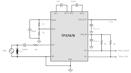
Because the cap drop solution is such a common power-supply configuration in Industrial applications such as e-metering and factory automation, TI has developed a component focused around optimizing the efficiency and solution size of a capacitive drop architecture. The TPS7A78 integrates many of the discrete components required to implement a capacitive dropper circuit, like the active bridge rectifier. Being designed to specifically operate using a capacitive drop circuit, the TPS7A78 can integrate several features that improve overall system efficiency. For example, the TPS7A78 incorporates a switch capacitor stage that reduces the input voltage by a factor of four, thus reducing the input current by the same ratio and facilitating the use of a smaller capacitive drop capacitor. This feature enables a smaller solution size, lowers system cost and reduces standby power.

Figure 3: 30mA Cap drop solution using the TPS7A78 at 30mA

To understand how much better the efficiency can be using the TPS7A78 over a cap drop stage and Linear Regulator let’s compare the traditional solution shown in Figure 2 with the TPS7A78 solution shown in Figure 3. In the traditional cap drop solution using a Linear Regulator the system has an efficiency of 11%. The TPS7A78 when configured to power the same load is able to achieve an efficiency of >40% due to the reduced input current from the switch cap and the need for a smaller surge resistor.

Additional resources:

Minimize the impact of the MLCC shortage on your power application

$
0
0

There is a growing shortage of multilayer ceramic capacitors (MLCCs), and the situation is likely to persist through 2020. MLCCs are used in almost every type of electronic equipment, due to their reliability and small footprint.

While MLCC manufacturers are taking action to increase their production capacity, demand is still expected to outpace supply, resulting in supply-chain shortages and increased prices for these components.

As a power application designer, you might be wondering about how to minimize MLCC supply risks while the supply chain adapts. In this blog post, I’ll discuss several options to power a typical industrial application rail, and show how selecting the right DC/DC converter can help minimize the impact of the MLCC shortage on the production of your product.

Let’s assume that you’re looking to convert a typical 12-V input voltage into a 3.3-V regulated output, able to deliver 3 A of current. With these parameters, TI’s buck converters quick search will propose several DC/DC converter alternatives for you to choose from for an industrial application. Appropriate solutions will offer excellent thermal performance in a compact quad flat no-lead (QFN) package and efficiencies close to or even above the 90% mark at those conditions. However, specifically looking at the required MLCC count for proper operation, there will be important differences that you will have to consider.

Let’s break down a typical externally compensated peak-current-control topology solution. You’ll need a small (0.1 µF) bootstrap capacitor to provide the gate voltage for the high-side metal-oxide semiconductor field-effect transistor, up to four capacitors (two 10 µF and two 0.1 µF) at the input, and a bigger (100 µF) capacitor at the output. A soft-start capacitor to control the output voltage startup ramp could be necessary, as well as two compensation capacitors for the frequency compensation network. This brings the total MLCC count up to nine for a typical circuit.

Another proposal is the TPS62136, a 3-V to 17-V input, 4-A step-down converter with the DCS-Control topology in a tiny 3-mm by 2-mm QFN package. The higher operating bandwidth and internal compensation of the TPS62136’s DCS-Control topology will enable you to minimize the output capacitor value and significantly reduce the total MLCC component count. The device’s evaluation module includes two 22-µF output capacitors only. A single 10-µF capacitor will suffice at the input, and no bootstrap or compensation capacitor is required. The use of a soft-start capacitor brings the total MLCC count to only four.

The TPS62136 comes in a package with low thermal resistance and gives efficiency close to the 90% mark for the stated conditions. It requires less than half the number of ceramic capacitors and creates a much smaller total solution size than a typical externally compensated, peak-current-mode control device. Figure 1 compares the number of required MLCCs for the circuit configurations discussed.

             Typical circuit schematics for an externally compensated peak-current-mode control device

Figure 1: Typical circuit schematics for an externally compensated peak-current-mode control device (a); and the TPS62136 (b); the required MLCCs are highlighted in red

If you’re looking to reduce the exposure of your power application to MLCC shortage issues, make sure that the DC/DC converter you select allows you to optimize both total capacitor value and count. Our high-operating-bandwidth DCS-Control topology converter portfolio, including the TPS62136, can help without sacrificing performance.

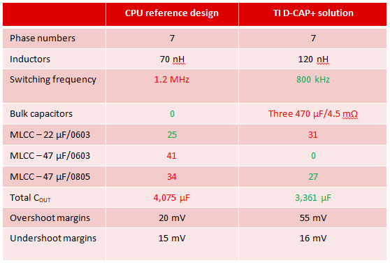
Next week, my colleague George Lakkas will show you how TI’s D-CAP+™ control mode multiphase controllers, converters and modules, including the TPSM831D31, can help you reduce the MLCC count on your motherboard versus competitive solutions.


No avalanche? No problem! GaN FETs are surge robust

$
0
0

We live in silicon-dominated world that shapes our thinking. I find it interesting to imagine an alternate universe where the gallium nitride (GaN) power field-effect transistor (FET) was developed before the silicon FET. Our power converters would certainly have been smaller and more efficient, but more importantly, we’d have been thinking differently.

Take for example the issue of avalanche rating. This parameter relates to the ability of silicon power FETs to survive power-line disturbances caused by lightning strikes or other abnormal occurrences.

The ability to survive a power-line surge is important for any power device. There is concern about the surge-robustness of present-day GaN FETs due to their lack of an avalanche rating. Many of us know Albert Einstein’s quote, “We cannot solve our problems with the same thinking we used when we created them,” and I believe this is good advice. The use of avalanche ratings for surge robustness arose because silicon power FETs do not typically possess much voltage headroom above their maximum voltage rating. When a power-line surge hits, the FET starts breaking down by impact-ionization phenomena, or “avalanche breakdown.” Over the years, the industry engineered the FETs to do this robustly, and the avalanching property has become associated with power-line surge protection. If silicon FETs had been able to switch through surge events, then the thinking would have been different. So let’s rethink surge robustness in a GaN-powered world.

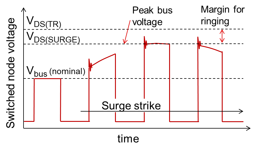
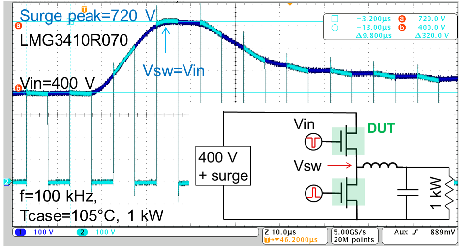
A technical paper at the 2019 IEEE International Reliability Physics Symposium (IRPS) describes the validation of the TI LMG3410R070’s surge robustness. GaN’s superior transient overvoltage capability enables GaN FETs to switch through surge events without avalanching and provides an additional design parameter: a transient surge-voltage rating, VDS(SURGE), which is the peak bus voltage that the FETs can withstand during active operation. A good value was determined to be 720 V, both from customer feedback and through system-level simulation.

Figure 1 illustrates the VDS(SURGE) definition, in coordination with the VDS(TR) parameter already in use on some data sheets. Using these parameters, you can easily limit the peak bus voltage at the device to 720 V during a surge event, as demonstrated in the IRPS paper.

 Figure 1: The surge rating parameter, VDS(SURGE), is the peak bus FET withstand voltage during operation when a surge strikes. Some GaN data sheets already have an off-state transient overvoltage parameter, VDS(TR), that serves to provide additional margin for ringing.
 

Figure 2 shows the switching of the LMG3410R070 through a surge strike, with the validation circuit in the inset. The circuit is powering a 1-kW load under regular operating conditions. The surge generator provides an International Electrotechnical Commission (IEC) 61000-4-5 industry-standard surge waveform, and is set so that the bus voltage at the GaN FETs surges to a peak of 720 V. The input and switched-node waveforms are overlaid to show the GaN FETs actively switching through the strike; switching at 720 V. The test consisted of 50 such strikes per the Verband der Elektrotechnik (VDE) 0884-11 standard while actively powering the load. There was no loss of efficiency, and neither the high- nor low-side GaN FET showed hard failure, demonstrating that they are surge-robust in power supplies.

Figure 2: Demonstration of the surge robustness of the LMG3410R070. The input bus voltage surges from the operating point of 400 V to the target specification of 720 V when the active circuit (inset) is struck with a surge waveform conforming to the IEC 61000-4-5 standard. The switched-node waveform is overlaid on the input waveform to show that the GaN FETs successfully switch through a 720-V peak bus voltage surge.

At TI, we take all aspects of GaN reliability seriously. TI has leveraged its many decades of silicon technology development – while recognizing the new opportunities that GaN brings – to think differently on how to deliver a robust and reliable power solution. Hard-switching the GaN FET in the early stages of technology development is critical, as described in the white paper, “A comprehensive methodology to qualify the reliability of GaN products.” Our recognition of the need for the industry to collaborate, as explored in the blog, “Let’s GaN together, reliably,” led us to help form the Joint Electron Device Engineering Council JC70 committee on wide-bandgap semiconductors. We have invested 20 million device hours in the reliability testing of GaN, including surge robustness.

I would love to imagine how the industry would react to a newly invented silicon power MOSFET in a GaN universe: “A silicon power MOSFET does not switch through surge – it avalanches?

4 Reasons why you should use a boost charger for 2-cell battery application

$
0
0

Finding the perfect battery charger integrated circuit (IC) for your portable electronic device design is not always easy, especially when you need a battery with more than one cell in series (1S) for higher voltages while achieving fast, cool charging in a small board area. In such cases, a boost charger may be what you are looking for. Here are four reasons why you should consider using a boost charger.

1. Boost chargers allow you to take full advantage of 5-V USB’s convenience.

Let’s look at one of the most widely adopted charging inputs in portable electronics – the USB charging port. Remember when every portable device had a different kind of adapter, with barrel-jack charging ports? As USB charging ports became mainstream, it’s now possible for consumers to carry only one adapter and a couple of cables for all of their electronics. USB charging has truly become a way of life.

A 5-V USB adapter and cable (either with a Micro B or a USB Type-C™ port) are cost-effective due to the large number of equipment suppliers; sometimes manufacturers can even exclude adapters from the product box because consumers already own one. A 5-V USB can be designed with up to 15 W of power with USB Type-C, which is enough for most small-size applications.

Using a 5-V USB with a two cells in series (2S) battery is a popular charging combination and a boost charger is required to make this happen. Why? Because it not only takes a 5-V USB input and boosts it up to charge a lithium-ion (Li-ion) battery with 2S, but a high performance boost charger does so in a highly integrated and efficient way, allowing you to get the most out of your portable device designs.

2.  Get the most out of 2S configurations with a boost charger.

Many battery-powered devices use 1S batteries to keep products simple and cost-effective. However, if the system includes higher-voltage blocks, you will need a boost converter to jack up the 1S battery voltage to power them. With a 2S battery and a higher voltage, you can exclude a boost converter and get a longer battery run time.

Applications in which 2S batteries could help include electronic point-of-sale devices or portable photo printers where systems may need a high-voltage print head. Additionally, wireless smart speakers might need a high voltage to supply dynamic current pulses to audio amplifiers, or a small power tool might use a 2S battery to drive the motor effectively and powerfully. An example of a typical 5-V USB 2S battery boost charging system is shown below in Figure 1.

It is also challenging to operate a Li-ion battery (specifically 1S) at low temperatures, as its internal impedance can increase dramatically. In smart home applications used outdoors, like wireless security cameras and video doorbells, when the temperature approaches 0°C, increased battery internal impedance will cause a significant reduction in the battery’s output voltage. The 2S battery configuration provides more voltage headroom to play with.

Figure 1: A boost charger in a 5-V USB 2S battery system

3. Integration eliminates the need to choose between a simple bill of materials or increased functionality.

The integration of boost charging solutions makes the design process simple, with loaded features in a small size.

Do you want your system to turn on instantly when the user plugs in an adapter, even with a depleted battery? Do you want to extend battery life? If the answer to either of these questions is yes, an integrated power path will help you reach your goals. The power path manages the battery’s field-effect transistor (FET) between the system and the battery. This feature guarantees a minimal system voltage so that the system can start when the battery is low, giving the device an instant-on feature. The power path also reliably cuts off the trickle charge when the battery is full to avoid overcharging, thus protecting the battery and extending its life.

A USB Micro B adapter uses D+ and D- to indicate its power sourcing capability. TI boost chargers integrate D+/D- (or DP/DM) detection and can configure the charger’s input current limit when the adapter plugs in. If the adapter is not a standard USB, advanced algorithms like the Vin Dynamic Power Management (VINDPM) and Input Current Optimization (ICO) will help the device detect the adapter’s maximum current capability.

There are more features you can use to make a great charging system. The USB On-The-Go (OTG) feature powers a peripheral device connected to the USB. In OTG mode, the boost charger operates reversely as a buck converter to provide a 5-V bus voltage to the attached device with a current limit. This function saves a buck converter, an inductor and sometimes a power switch. The internal analog-to-digital converter keeps the system aware of what’s going on around and inside the IC. The integrated AC overvoltage protection FET protects the system from input overvoltage events. Figure 2 illustrates the BQ25883, our new boost charger that integrates the power path, D+/D- detection and OTG, among other special features, into one IC.

Figure 2: BQ25883 boost charger system diagram

4. Select the right boost charger for your unique considerations.

Our new boost charger family, BQ25882, BQ25883, BQ25886, BQ25887, provides several options to meet your application requirements. I2C chargers offer great flexibility by setting and changing the charge profile with software and by providing charging status to the system host. The stand-alone charger enables an easy charging setup with external resistors. The cell-balancing version employs an advanced algorithm to quickly balance the voltage of the two cells while charging within one cycle. This is an important feature for products that have two loose cells or that target a long battery life. You can see all of our boost charger family and each of their unique features in Table 1 below.

DeviceBQ25882BQ25883BQ25886BQ25887
VBUS operating range3.0 to 6.2 V3.9 to 6.2 V4.3 to 6.2 V3.9 to 6.2 V

USB detection

D+/D-D+/D-D+/D-PSEL
Power pathYesYesYesNo
Cell balancingNoNoNoYes
OTGUp to 2 AUp to 2 AUp to 2 ANo OTG
16 bit ADCYesYesNoYes
Control interfaceI2CI2CStandaloneI2C
Status pin/PGSTAT , /PGSTAT , /PGSTAT , /PG
Package2.1x2.1 WCSP-25 4x4 QFN-244x4 QFN-244x4 QFN-24

Table 1: TI boost charger family comparison table

 Conclusion

We understand that each portable device design has unique considerations and we want to make it easy to choose the best charger for your design. These four points express the benefits of using a boost charger with 5-V USBs and 2S batteries. We hope you consider a boost charger in the future for a convenient and high performance product.

Additional resources

Minimize the impact of the MLCC shortage using D-CAP+™ control mode

$
0
0

As my colleague Yann said in an earlier blog, there is a growing shortage of multilayer ceramic capacitors (MLCCs), and the situation is likely to persist through 2020. MLCCs are used in almost every type of electronic equipment, due to their reliability and small footprint.

Manufacturers are now looking to replace ceramic capacitors with polymer or other capacitor types. TI D-CAP+™ control mode multiphase controllers, converters and modules (like the TPSM831D31) can help hardware designers reduce the MLCC count on their motherboard versus competitive solutions.

D-CAP+ control mode is a TI proprietary pulse-width modulation controller and converter control architecture that enables very easy loop compensation and excellent loop stability in the presence of varying conditions such as input voltage and the number of phases.

It is a current-mode constant on-time control that uses a true inductor current-sense implementation rather than the injected or emulated ripple current schemes used in the D-CAP2™ and D-CAP3™ control topologies. The D-CAP+ control mode has fixed on-time in steady state and adaptive on-time during load transient condition (AC response), in which the field-effect transistor switch rapidly adjustsas the input and output voltage change to maintain a constant overall switching frequency.

Since the on-time is regulated, there’s a natural period stretching in discontinuous conduction mode (DCM), producing higher efficiency and smooth control when crossing the continuous conduction mode and DCM boundary. D-CAP+ control mode is extremely easy to compensate and does not require the complex type-3 compensation circuits required in voltage-mode control architectures. For more information on D-CAP+ control mode, see the 2014 Power Supply Design Seminar paper, “Choosing the Right Variable Frequency Bulk Regulator Control Strategy

Because D-CAP+ control mode can respond much faster to a processor/application-specific integrated circuit/field-programmable gate array load transient than a fixed-frequency control architecture, it can meet tight tolerance specifications without the number of MLCCs that you would otherwise need for discharging or charging to provide the required energy to the load.

Figure 1 compares a TI voltage-mode controller vs. a D-CAP+ controller during such a load transient. The TPS53647 D-CAP+ control-mode controller has lower overshoot and undershoot, despite having a lower crossover frequency.

Figure 1: Load transient response comparison between voltage-mode and D-CAP+ controllers

The results are similar when making comparisons to competing multiphase controllers with non-D-CAP+ control. Figure 2 compares a 60-A load step from 180 A to 240 A at a 1-kHz load transient repetition rate. The D-CAP+ controller, again, results in lower overshoot and undershoot. These results were replicated on the same motherboard under the exact same conditions. The TPS53681 D-CAP+ controller can achieve better load transient response and faster output voltage settling.

Figure 2: Load transient response comparison between a competing device and TI’s D-CAP+ controller

As a final example, let’s compare a central processing unit (CPU) vendor’s reference design to our own Vcore design. The thermal design current (TDC) was 116 A, while the maximum current (IMAX) was 395 A.

The test data shows that the D-CAP+ controller enables a faster load transient response, which translates to significant MLCC savings vs. the CPU vendor reference design.

Table 1 summarizes the results. The D-CAP+ control solution still meets the CPU overshoot and undershoot specifications while eliminating 42 MLCCs and >700 µF of output capacitance. The Table 1 comparison is applicable to any D-CAP+ control-mode voltage regulator vs. competing regulators.


Table 1: CPU reference design vs. D-CAP+ solution MLCC count comparison for a 116-A TDC and 395 IMAX design

MLCC shortages are not going away anytime soon. If you want to reduce the MLCC count in your design bill of materials so that you can get new projects to market faster, consider using TI’s D-CAP+ controllers, converters and modules.

Additional resources

Battery-charging tips for video doorbell applications

$
0
0

video doorbell

Figure 1: Video-enabled doorbell

Our homes are getting smarter and connecting to the internet with security cameras, thermostats, smart speakers and smart TVs. The video doorbell, seen in Figure 1, is another smart device gaining popularity, providing high-definition images and two-way audio communication so that homeowners can greet visitors from their smartphone. Video, activated by a motion sensor, records activities in the front and back yards, enhancing home security around the clock and through any weather conditions. While most video doorbells are hardwired, many consumers are seeking battery-powered video doorbells when the existing wiring or transformer is out of date or incompatible. A battery-powered video doorbell also provides convenience for renters who can’t (or shouldn’t) touch the wiring. Such doorbells are easily installed in flexible locations with no wiring needed. Another benefit is that battery-powered video doorbells keep working even during power failures.

Figure 2 shows a typical video doorbell battery charging system and the design considerations. These are the main design challenges for battery-powered subsystems in video doorbells:

  • Deciding the battery configuration based on the operating temperature.
  • Optimizing system solution cost with USB charging.
  • Maximum utilization of the input source to reduce the charging time
  • Achieving a small form factor with integration.
  • Acquiring an accurate percentage of remaining battery capacity.

Figure 2: A typical battery charging system and the design considerations.  

Video doorbells need to operate under different weather conditions, so you need to consider the operating temperature of the battery when choosing between lead-acid, nickel-metal hydride or lithium-ion (Li-ion) chemistries and configurations. Due to multiple factors – including the need for a small form factor, the power required for the system and the frequency of recharging – Li-ion-based batteries still remain the best option in terms of power density and cost.

However, the internal impedance of a Li-ion battery could increase dramatically under low-temperature conditions. A reduced battery terminal voltage (due to the internal impedance) could prevent the energy stored in the battery from powering up the system with the required current. A single-cell (1S) battery’s internal impedance increases quickly when the temperature approaches 0°C. In order to provide a system voltage at a wider temperature range, doubling the battery voltage by placing two batteries in series (2S) provides much more voltage headroom for the battery to discharge before reaching the minimum voltage to power the system.

Whether you adopt a 1S or 2S battery configuration, you still need an adapter or cradle-type charging station to charge the battery. Traditionally, an adapter is a must have e accessory in a video doorbell package. It would be a significant advantage to charge the battery easily with USB power, which is easily available in most households. In order to achieve universal charging of 1S and 2S batteries with USB as the input, considering the battery charger topology and detection of the USB port current capability are two important technical challenges, respectively.

First, the charger topology will differ. A 1S battery requires a step-down topology for 5 V to charge a 1S battery. A 2S battery requires a step-up boost topology from the 5-V USB to charge 2S batteries. Second, battery charging specification revision 1.2 (BC1.2) provides the standard and procedure to use the USB D+ and D- lines to detect USB port current capability. The section of input source type detection on TI’s BQ25882 data sheet gives an example of a battery charger following BC1.2 to detect input USB sources. With USB detection, the charger can take any USB port as the input to charge the battery, with maximum utilization of the input source.


Enabling the next generation of video doorbells


Read the white paper here

The size of a video doorbell cannot be much bigger than a traditional doorbell, and consumers also want several months of uninterrupted service time before recharging the battery. A capacity of around 15 Wh to 22 Wh is the current range. Some consumers complain online that their batteries need a charging time of eight or more hours; the goal is to get the battery fully charged in a more reasonable three to four hours.

Maintaining good thermal condition of the battery pack provides a good customer experience. Integration and charging efficiency are also important considerations. Fully integrated chargers with all of the required metal-oxide semiconductor field-effect transistors (MOSFETs), current-sensing elements and protection functions can reduce bill-of-materials (BOM) cost.

High efficiency is key to reducing the power loss to improve thermal conditions. First estimate how much power loss the doorbell or the battery pack can dissipate. Based on the loss budget, estimate the efficiency and check the efficiency curve to identify the right chargers for your application.

After figuring out how to get the energy into the battery, it is very important to obtain an accurate representation of how much energy has already been placed into the battery. Thus, having an accurate gauging device becomes important so that consumers are aware that the battery needs charging. TI is a leading expert in battery gauging with its Impedance Track™ algorithm.

TI’s charging, gauging and protection solutions for various applications include video doorbells. If you have more questions, see the technical information for the BQ25601D and BQ25895 fully integrated 1S chargers with USB detection or the BQ25882 2S battery boost charger with USB detection.

Additional resources

  • Battery charger: 1S fully integrated chargers with USB detection BQ25601D and BQ25895; 2S fully integrated boost charger BQ25882 with USB detection
  • Battery gauge: compensated end-of-discharge voltage (CEDV) gauge BQ27220
  • Battery protector: 1S primary protector BQ2970 and BQ29800 and 2S secondary protector BQ29209

Improvements in solar power efficiency come from the smallest gate drivers

$
0
0

Climate change has been a subject of much debate the past 10-30 years, sparking political discussions on what types of regulations are necessary. In the short term, it’s significantly more expensive to develop a greener infrastructure that moves away from relatively cheap energy sources like fossil fuels.

Government subsidies are designed to encourage growth in renewable energy technologies. These subsidies allow companies working on renewable technologies to remain competitive with traditional energy companies, who control the majority of the market. They allow governments to help spark environmental change through private companies in an effort to help future generations, while limiting regulations or taxes on traditional energy sources. Solar power is a great example of a renewable technology that can disrupt the traditional energy market.

Solar panels capture the sun’s energy and convert it to DC energy. The DC from the panel must be converted or boosted up to a higher voltage, which then is converted to AC through inverters. Once converted to AC, the electricity can be used by households, buildings, plants, etc., or sent directly to the electrical grid.

For solar power to be a worthwhile investment, the solar panels must be extremely efficient in converting solar energy to usable electricity. To do this, companies have designed devices to help maximize the energy harvested by solar panels: solar power optimizers and microinverters. Solar power optimizers installed on each solar panel are used to condition DC energy before it’s sent to a central inverter for conversion to AC energy. Like solar power optimizers, microinverters are also placed on each solar panel, but they convert DC energy to AC energy directly on the solar panel. Although these technologies differ, they have the same goals: improve individual solar panel performance to help increase energy production by the entire system.

What does this have to do with semiconductors? The smallest decisions in design and layout can impact the efficiency of both microinverters and solar power optimizers. One of these small but vastly important decisions revolves around the metal-oxide semiconductor field-effect transistor (MOSFET). See Figure 1.

Figure 1: Highly Efficient, Versatile Bi-Directional Power Converter for Energy Storage and DC Home Solutions reference design

The solar power optimizer shown in Figure 1 shows the job of the MOSFET, which is to condition the voltage from the solar panel’s photovoltaic cells (PV+/PV-) before sending it to a central inverter (String+/String-) to finish the DC/AC conversion. These MOSFETs need to be able to reach high voltages during DC/DC conversions and thus need a gate driver because the FETs cannot be driven directly by a microcontroller.

TI’s 120 V, 3.5 A, UCC27282 gate driver is a good fit for this situation. The 3-mm-by-3-mm gate driver was designed to drive two N-channel MOSFETs in high-side, low-side configurations. Since the MOSFETs are in an H-bridge configuration, the UCC27282 can quickly switch the corresponding gates, which are used to convert lower voltages to high voltages.

Solar power optimizers also benefit from the safety features built into the UCC27282. Undervoltage lockout (UVLO) is a protection feature that inhibits each output until a sufficient supply voltage is available to turn on the external MOSFETs. The UCC27282 has a 5 V UVLO, the lowest of any current TI half-bridge gate drivers. This is helpful during startup when a sufficient voltage hasn’t been established and the DC supply voltage (VDD) doesn’t exceed the UVLO threshold.

Without UVLO, a MOSFET can be turned on with an insufficient voltage that could damage the FET and the entire system. If the FET is not fully turned on, the device will have a high resistance during conduction and will dissipate the power as heat. Additionally, a MOSFET could be driven into an unknown state, where the FET may not switch when desired, resulting in a system not acting as anticipated. The UVLO for the UCC27282 is 5 V, the lowest of any current half-bridge gate drivers.

Another advantage of 5 V UVLO is that it makes it possible to use a lower VDD, which helps increase efficiency because it decreases switching losses. A lower VDD also enables more flexibility for optimizing total MOSFET losses.

Because of the frequent switching of the MOSFETs in solar applications, switching noise can be felt on the input stage of the gate driver. If this occurs, the integrity of the input signal could be disrupted, causing two inputs to be high at the same time. The UCC27282’s input interlock, also known as cross-conduction protection, prevents this error at the inputs from being reflected at the outputs and causing damage to the power stage.

A final performance feature that could help boost efficiency in solar power optimizers is an enable/disable pin. Power optimizers use maximum power point tracking for each individual module to ensure DC/DC conversion is performed in the ideal power-harvesting range. Once out of the ideal power-harvesting range, the UCC27282 is not needed for DC/DC conversion and its enable functionality can be used to reduce quiescent (standby) current losses.

In the solar energy field, the smallest increases in efficiency are difficult to achieve. The slightest changes from some of the smallest devices in the design can make all the difference. While just a few percentage-point increases in efficiency may seem inconsequential, they’re necessary to gain market share from traditional fossil-fuel energy sources. Any gains made by renewable energy sources help create a cleaner society, which benefits future generations.

Viewing all 437 articles
Browse latest View live


<script src="https://jsc.adskeeper.com/r/s/rssing.com.1596347.js" async> </script>