Quantcast
Channel: Power management
Viewing all 437 articles
Browse latest View live

Choosing the right flyback controller for your design

$
0
0

If every industry has one common goal, it’s the push to do more with less. How do you make something lighter, smaller, faster and stronger? Power is no exception.

With the ever-increasing demand for smaller power supplies to do more, designers have adapted by integrating key features that boost efficiency while saving space and budget. In order to meet modern requirements, power-supply controllers evolved from a few general-purpose controllers to a large portfolio of application-specific controllers. In the past, any designer looking to build consumer chargers found a general-purpose pulse-width modulation (PWM) controller a great solution for their needs.

Today, that same consumer charger requires a specialized flyback controller to meet regulatory requirements such as Department of Energy (DoE) Level VI and Code of Conduct (CoC) Tier 2. These flyback controllers have advanced features, like AM/FM control laws, that help them achieve high efficiency and power density. On the other hand, advanced features can cause the price to skyrocket.

For charger applications that require low standby power, having a controller with an integrated startup high-voltage field-effect transistor (FET) is worth the cost. But for applications like electricity meters, smoke detectors or electric vehicle (EV) charging piles, this feature is overkill. Although the improved performance is nice, it can cause the cost of the power supply to become prohibitively expensive.

TI’s flyback controllers mix and match various features to meet the specifics of your design, whether you need to prioritize your budget or efficiency or density requirements. Table 1 lists frequently used flyback controllers.

Table 1: Flyback controller family highlights

But how do you differentiate between these devices? Even controllers that seem very similar may make a difference in an application. For example, the UCC28742 is in a smaller package than the UCC28740 and does not have the high-voltage pin 700V startup FET included in UCC28740’s larger package. For devices that do not need to meet a ≤10mW standard, the UCC28742 will save space and budget. However, if meeting this standard is one of your requirements, you would select the UCC28740. The UCC28742 might be preferable in applications such as electricity meters, smoke detectors and small household appliances, while the UCC28740 might be a better choice for charger applications.

Overall, these devices, like the rest of the flyback family, use the same control laws and features that result in highly efficient controllers with reduced generated electromagnetic interference (EMI) and robust fault conditions.

To learn more about TI’s AC/DC flyback family and find out which device is for you, see ti.com/flyback and check out these resources:


Use a low-quiescent-current switcher for high-voltage conversion

$
0
0

In battery-operated environments, it’s important to pay attention to quiescent current when designing your power system block diagram. Some applications, such as cordless handheld garden tools, lighting controls and cordless lawnmowers, have low-quiescent-current specifications.


These tools operate with a battery pack that has an operating voltage range from 12V to 48V or higher. Using a low-dropout regulator (LDO) to convert this higher battery voltage to a lower voltage would increase power dissipation in the pass device transistor and drain the battery faster when the standby load current is large. For example, if you have a 48V battery pack and try to convert it down to a 5V or 3.3V rail, then the conversion efficiency is roughly VOUT/VIN, which in a 5V output case will be 10.4%. The input current drained from the battery will be the same as the output current.


Let’s say that your standby current for all monitoring peripherals is 5-10mA; this current would drain out of the battery directly if you just used an LDO. A DC/DC converter reduces the input current consumption because of the switching action of the internal field-effect transistors (FETs).


Figure 1 shows the input current data for an LM5165 DC/DC converter over the input voltage and load current ranges.


Figure 1: Input current of the LM5165 at different load currents


As you can see, at a 48V input voltage and 10mA load current, the input current consumption from the converter is around 1.3mA. This is almost a one-tenth current reduction compared to a single LDO stage, where a load current of 10mA would require an input current of 10mA.


The periodic switching of the converter causes lower current consumption at the input. Figure 2, taken from the LM5165 synchronous buck converter data sheet, shows that at no load the device does not switch continuously; instead, it waits a certain period before it switches again. Figure 2a is at a no-load condition and Figure 2b was taken at a 25mA load current.


Figure 2: Switching waveform at no load (a); and a 25mA load (b)


The LM5165 has the flexibility for you to create a power design tree for a handheld cordless tool like that shown in Figure 3.


Figure 3: Example of a high-voltage handheld cordless tool battery power conversion diagram


Battery-operated devices sometimes also require a small solution size. Figure 4 shows how the LM5165 evaluation module for a 5V, 25mA output current can fit into a 12mm-by-15mm package.

Figure 4: LM5165 evaluation module size comparison


As you can see, it’s possible to use a low-quiescent-current switcher to boost overall system efficiency for high-voltage conversion. If you still need an LDO for its low-noise advantages, an extra DC/DC converter stage can reduce the input current that will drain from the battery.

How to add overvoltage protection to a synchronous boost controller

$
0
0

Although a cycle-by-cycle current-limit function exists in most synchronous boost controllers, sometimes engineers will add output overvoltage protection (OVP) in case of emergency to protect discrete circuits. In this blog post, I’ll show you how to achieve accurate output OVP at a very low cost. Although I’ll use the LM5122 synchronous boost controller and its evaluation module (EVM) as an example, the proposed circuits are applicable to other synchronous boost controllers.

The LM5122 multiphase synchronous boost controller is intended for high-efficiency synchronous boost regulator applications. Its control method is based on peak-current-mode control, which provides inherent line feed forward, cycle-by-cycle current limits and easy loop compensation. Figure 1 shows the simplified LM5122 application diagram. Although the cycle-by-cycle current limit function exists, the LM5122 doesn’t provide OVP itself. However, by adding a simple circuit you can achieve accurate-enough output over voltage protection.

Figure 1: Simplified LM5122 application diagram

Figure 2 shows a primitive output OVP circuit where the output voltage sense resistor divider consists of R1 and R2. Assuming that Vz is the breakdown voltage of the Zener diode, Vbe is the voltage that falls between the base and emitter of the n-channel p-channel n-channel (NPN) transistor. You can use Equations 1 and 2 to trigger the circuit to run into protection:


Because Vz and Vbe normally have tolerance and they also vary over temperature, the OVP threshold will vary widely.

Figure 3 shows another output OVP circuit, which will have more controlled OVP threshold. Again, the output voltage sense resistor divider consists of R1 and R2. The LMV431 is a low-voltage (1.24V) shunt regulator. By comparing the central point of the sense resistor divider and the internal reference pin of the LMV431, OVP will trigger if the central point voltage of the sense resistor divider is higher than the 1.24V reference, as expressed in Equation 3:


Because the LMV431 has an initial small tolerance of 1.5% over temperature, this circuit has more OVP precision than the primitive output OVP circuit with the Zener diode. If the central point voltage of the sense resistor divider is higher than 1.24V, the cathode voltage of the LMV431 decreases, which will cause the base of the MMBT2222 to be high. The collector of the MMTB2222 connects to the undervoltage lockout (UVLO) pin of the LM5122 and the UVLO pin pulls down to 0V. The boost converter enters shutdown mode and stops transferring energy to the output.

Figure 2: Primitive output OVP

Figure 3: Output OVP circuit

Using the LM5122 EVM, the OVP voltage is set to 23.5V. In order to verify the OVP circuit, you can adjust the EVM to set the nominal VO as 19.5V, with an additional 10kΩ resistor added to the VO sensing divider. Figure 4 shows the experimental result. LO is the low-side N-channel MOSFET gate drive output. When VO increases to 23.5V after adding the 10kΩ resistor in parallel, the UVLO pulls down to zero and the LM5122 goes into shutdown mode, with all functions disabled.

Figure 4: Low-side MOSFET stops switching when OVP triggers

The reason that you need to use two MMBT2222 and MMBT2907 transistors is because the LM5122 UVLO threshold is 1.2V. The minimum voltage of the LMV431 cathode is above 1.24V. Adding these two transistors will cause the UVLO pin under 1.2V to stop switching.

Figure 5 shows another simplified output OVP circuit without two transistors. The LM5122 controller features a UVLO function, with an external UVLO setpoint voltage divider from the supply voltage VIN to the analog ground pin (AGND). The LM5122 evaluation module has a startup voltage of 8.7V and VHYS is set to 0.5V. The standard value of RUV2 is 49.9kΩ and the standard value of RUV1 is 8.06kΩ. By splitting RUV2 into two resistors RUV2_1, RUV2_2 and connecting the cathode of the LMV431 to the central points of these two resistors RUV2_1, RUV2_2, you can achieve the similar output OVP feature with circuit shown in Figure 3.

Figure 5: Simplified output OVP circuit

Figure 6 shows the experimental result of the second output OVP circuit. When VO increases to 23.5V, the cathode voltage of the LMV431 decreases to 1.24V and the UVLO pin voltage becomes 0.53V. The LM5122 enters standby mode and stops switching. The soft-start capacitor discharges to 0V and after a 5.9ms soft-start time, the device starts switching again. The second output OVP circuit triggers standby mode and is cheaper than the first OVP circuit.

Figure 6: Low-side MOSFET stops switching when OVP triggers

Conclusion

The two output OVP circuits I proposed in this post have a more accurate OVP threshold compared to the primitive OVP circuit. The second OVP circuit can help you build an easier and low-cost output OVP function for a synchronous boost controller. Download the LM5122 evaluation module now and start your design.

How to achieve higher system robustness in DC drives, part 3: minimum input pulse

$
0
0

Have you ever been watching your favorite show and noticed a blur or partial screen freeze? I think it was caused by an incorrect timing of the refresh.

For proper operation in a half-bridge power train, such as DC drives, it is important that the timing to the high and low-side power devices is correct. In the case of watching TV, a timing glitch is just annoying. But in a half-bridge power train, timing glitches in the high-side and low-side power devices can interrupt the intended operation, or even cause a failure in half-bridge power metal oxide semiconductor field effect transistors (MOSFETs).

There are important design details to consider in order to achieve higher system robustness when selecting a gate driver for your DC drives. In part 1 of this series (How to achieve higher system robustness in DC drives part 1: negative voltage) German Aguirre discussed negative voltage spikes on the switch-node HS pin, and in part 2 of this series (How to achieve higher system robustness in dc drives part 2 interlock and deadtime) I discussed output interlock and deadtime. In this installment, I’ll discuss the minimum input pulse rejection feature.

Minimum input pulse rejection prevents the outputs (LO and HO) from responding to a pulse width less than the allowable minimum input pulse requirement, thus preventing the driver outputs from responding to narrow spikes or ringing, generating an unexpected driver output pulse, and having the MOSFETs from turn on at the incorrect time.

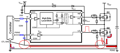
Voltage spikes and ringing on the driver input signals caused by current spikes flowing in the control ground paths are a common problem in motor control. Figure 1 shows the board layout trace ground paths that exist in many designs. In many cases, it is not possible to eliminate the potential for current flowing in the control ground, so you will need a robust gate driver to handle the transients that they cause.

The red arrows in Figure 1 show low-side turn on during hard switching operation: the falling VDS voltage generates a current spike upon discharge of the switch node capacitance. This high dI/dt current spike will flow through the ground path and return to the input capacitance. As the driver ground (COM) typically connects close to the MOSFET source, and the controller in many cases connects to the driver ground, a parallel current path exists from the MOSFET source, (COM) and controller. This can result in a significant current spike flowing into the control-referenced ground.

Figure 1: Driver input voltage spikes/ringing from ground current

Adding a high-frequency impedance such as inductance or resistance to the path between the MOSFET source and the driver/controller ground reference can reduce the current flowing into the controller, as shown in Figure 2.

Figure 2: Impedance in ground path to reduce control ground current

It’s important that gate drivers have features that can tolerate voltage spikes in order to ensure reliable operation and improve robustness in your designs. The UCC27710 driver’s minimum input pulse feature prevents the LO and HO outputs from responding to narrow spikes and ringing. This driver rejects low to high pulses and high to low pulses less than 40ns as shown in Figure 3, and thus prevents driver input noise from causing the power MOSFETs to unexpectedly turn on or off. 

Figure 3: LO and HO response with positive and negative narrow pulses

Let’s look at ways to reduce ground current voltage spikes on the driver inputs. You can add resistance or inductance to reduce current in the control ground. This resistance or inductance creates a high-frequency impedance.

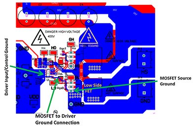
Figure 4 shows an example half-bridge driver and power-train layout. You can see that the low-side MOSFET connects to a large ground path and the driver input connects to a large ground path. But the large ground planes are not continuous from power to driver input or control.

Figure 4: MOSFET to control ground connection to limit current spike 

If the MOSFET source to control ground has a higher inductance than the power and control planes, the current spike will be reduced in this path relative to the large power plane. The narrower trace connection shown in Figure 4 will result in a higher inductance path.

In part 2 of this series (How to achieve higher system robustness in dc drives part 2 interlock and deadtime) I provided other layout tips on how to reduce noise on the driver inputs.

TI gate drivers with minimum input pulse rejection provide higher system robustness when designing motor drives.

Additional resources

Top three qualities to consider when designing a video doorbell power supply

$
0
0

By Natnael Weldegiorgis and Jim Broiles


With the increased use of smartphones and tablets, there is a lot of effort on integrating popular home technologies like the Google Nest thermostat and Amazon’s Echo Dot. Consequently, the safety and security that comes with smartphone integration is fueling large growth in different home automation sectors.

The video doorbell, which enables users to view the threshold of their homes remotely, is one rapidly growing sector of home automation. The demand for video doorbells is continuing to rise as more and more companies offer high-end and secure products for cheaper prices. One of the main reasons for this affordability is the balance between quality and price in the devices used to make the different technologies causing more manufacturers to venture into home automation.

When designing a video doorbell, you should look for three main qualities during front end power supply device selection. The first and most important feature is wide input range to support operating voltage due to different transformer rating ranging from 8V ~ 36V AC. It is vital for a video doorbell front end design to include power-management products that support high efficiency across wide input range and operating load current.

The process of efficient power use starts as the video doorbell receives a rectified pulsated DC voltage and must convert that value to a lower DC voltage. The LM76002 synchronous step-down voltage converter has a wide 3.5V to 60V input-voltage range and the capability of driving up to 2.5A. As Figure 1 shows, the LM76002, compared to a competing device, has even much higher light load efficiency. With higher efficiency, the LM76003 also brings with it a low standby quiescent current, which when used in a video doorbell design means minimal power use during wait time. This is important for video doorbell designs that have a battery.

Figure 1: Efficiency comparison chart


The second quality to look for when designing a video doorbell is thermal performance. In order to create a video doorbell that can be mounted on any door frame and perform its best in any temperature, you must consider the thermal performance of the power-management components. The LM76002 buck converter stays at a maximum temperature of 52°C at an ambient temperature of 25°C. The LM76002’s ability to stay at a lower temperature means that your video doorbell design can maximize space without any overheating concerns.

Figure 2 compares the LM76003’s thermal performance with a competing device after applying a full load and allowing both devices 15 minutes to reach thermal equilibrium.

Figure 2: Thermal efficiency comparison after applying full load


The third quality to look for when designing a video doorbell is the size of the power-management circuit design. In addition to its high efficiency and cooler thermal performance, the LM76003 is also small, measuring 4.1mm by 6.1mm. With a video doorbell design that encompasses a camera, Wi-Fi® connectivity and many other integral components of the system, it is important to be able to use a small power-management device. The major benefit when considering the small size of the integrated circuit is its ability to fit into a condensed video doorbell design that is easily mounted. Small video doorbells are also popular with consumers.

When designing small end equipment like a video doorbell that spends most its time on standby and must perform in different temperatures, the LM76002 synchronous step-down voltage converter is a good fit.

How to eliminate interference in wireless access point equipment

$
0
0

Equipping broadband modems, routers and gateways in home and enterprise networking with wireless access point (AP) functionality is experiencing explosive growth. Figure 1 shows such a Wi-Fi® network. As the market keeps growing, the DC/DC converters used in this kind of equipment must fulfill several requirements.

Figure 1: Typical residential or small office Wi-Fi network

The first requirement is at least a 1.2MHz switching frequency. Figure 2 shows a diagram of a wireless AP. The switching noise of the DC/DC converter powering the Wi-Fi core chip will affect the error vector magnitude (EVM) of that Wi-Fi modem, thus degrading the communication quality. Fortunately, standard Wi-Fi chipset phase-locked loops (PLLs) have a frequency response that can serve as a low-pass filter with a cutoff frequency at ~1MHz.

Experiments show that it’s possible to minimize this kind of EVM interference by using a high-frequency DC/DC converter. Most wireless AP chipset manufactures, like Qualcomm and Broadcom, suggested a minimum switching frequency higher than 1.2MHz, with some margin reserved.

Figure 2: Diagram of a wireless AP

To satisfy the minimum frequency requirement, you could use a converter based on current-mode control. This kind of converter usually has an internal clock to synchronize its operation. It’s not very challenging to meet a design target such as 1.4MHz with a tolerance ±200kHz. The disadvantage is the converter’s moderate load transient performance. Sometimes, to meet the fast load transient requirements of a Wi-Fi system, you have to use a larger output capacitance, which increases the total system cost.

The second requirement is the faster load transient response. The power consumption of the amplifier in a Wi-Fi block is quite different in the data transceiver and idle states, and the state change can be very fast. This imposes higher requirements on the load transient performance of your power-supply solution.

You could choose a converter with a constant on-time (COT) mode, which is famous for its faster loop response. Unfortunately, there is no internal clock in a COT converter; the converter simply generates a proper on-time for the high-side power field-effect transistor (FET) based on the input and output voltage to maintain a pseudo-constant switching frequency. The switching frequency of a COT converter changes greatly as the input and output voltage changes. It’s very difficult to design a COT converter with a relatively tight frequency tolerance requirement.

You need a high-frequency, cost-effective solution that has fast load transient performance like a COT converter, but can also maintain a relatively constant switching frequency like a current-mode converter.

Figure 3 illustrates a proposed solution that adopts the D-CAP3™ control mode and implements a proprietary frequency-lock function to achieve a constant frequency like a current-mode device.

Figure 3: Block diagram of a D-CAP3 control-mode-based converter

Compared with the traditional COT control mode, you can realize several benefits with this solution:

  • The converter switching frequency is compared to a reference clock frequency. Based on the result, the on-time generated by a one-shot block adjusts to maintain a switching frequency within a relatively narrow variation range.
  • An error amplifier removes DC voltage errors caused by the ripple amplitude of the output voltage. This DC error normally exists in a traditional COT control-mode converter.
  • Instead of using the ripple of the output voltage as in a COT converter, a D-CAP3 control-mode-based converter will generate an internal ripple signal to emulate the inductor current ripple, eliminating the need for an equivalent series resistor on the output capacitor and achieving stable regulation even without output voltage ripple.

The frequency lock function makes it possible to achieve a relatively constant switching frequency. If the internal reference clock is set to 1.4MHz, you can easily guarantee a switching frequency higher than 1.2MHz in mass production, satisfying the first requirement. As to the second requirement, you can also meet a fast load transient response easily, since that is an inherent benefit of DCAP-3 control mode.

Let’s take TI’s TPS563249 17V, 3A buck converter as an example to obtain the measurement result.

Figure 4 shows the faster load transient response of the TPS563249 compared to a current-mode converter. To make a direct comparison, the switching frequency of the current-mode converter is set at 1.4MHz, as is the TPS563249, and the crossover frequency is set at about one-tenth the switching frequency. Both converters are using the same 1.5µH/22µF output inductor-capacitor filter.

Figure 4: The faster load transient response of the TPS563249 compared to a current-mode-based converter

The load step is from 1A to 3A with a 2.5A/µS slew rate; the target output voltage is 3.3V. The peak-to-peak output voltage ripple with the current-mode converter is 4.3% of the nominal output voltage, while it’s only 2.3% with the TPS563249.

Figures 5 and 6 show the constant switching frequency of the TPS563249 compared to a general COT converter without the frequency lock feature.

Figure 5: Frequency variation versus a different VIN (VOUT = 5V)

Figure 6: Frequency variation versus a different VIN (VOUT = 1.05V)

The TPS563249 has a smaller variation range compared to a general COT converter. As you can see, the TPS563249 also maintains a tight frequency range: there is around 5% of variation from the nominal frequency regardless of how the input and output voltage changes. However, for the general COT converter, the frequency varies ~35% from the nominal frequency in the worst case.

In general, the TPS563249 works at a constant 1.4MHz switching frequency and removes the noise interference in a Wi-Fi system for all conditions. It also satisfies the fast load change requirement from a Wi-Fi amplifier by implementing D-CAP3 control mode.

The 1.4MHz high switching frequency is helpful to minimize total system size, as well as bill-of-materials cost. It’s quite suitable for frequency-sensitive applications, such as broadband modems, routers and gateways with wireless AP.

Additional resources

USB Type-C™ and USB Power Delivery – no assembly required

$
0
0

As USB Type-C™ and USB Power Delivery (PD) gain momentum across a broad set of products, more and more engineers are rolling up their sleeves and making plans to add USB Type-C to their newest designs. It can be a bit overwhelming to start a new design with a fairly new technology.

USB Type-C combines power, video and data on a single connector. Researching components and specifications of each new feature requires a great deal of time and skill. So I want to spend some time looking at a very complex use case and showcase how to build the solution with “no assembly required.”

First of all, what do I mean by no assembly required? It’s just a play on words to highlight the typical challenge associated with adding power, video and data to a single port. Assembly language is a tedious, time-consuming endeavor, and most non-TI solutions require a process that’s just as cumbersome. Engineers must write software or firmware to control the various aspects required to bring these three technologies together, and it really can get quite complex. After a detecting a USB Type-C cable, you’ll need to enable the appropriate power supply with the correct voltage; query the cable to identify its capabilities; determine the capabilities of the device on the far end; and configure both the external multiplexer and the DC/DC converter.

Easy, right?

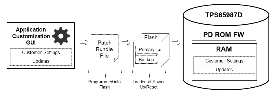
Well, it can be. TI does not expect you to learn how to program the TPS65987D, for example, or read mountains of USB specifications. The TPS65987D is a configurable device. Pre-programmed, Underwriters Laboratories (UL)/International Electrotechnical Commission (IEC)-certified and USB Implementers Forum-compliant, the TPS65987D requires only a few mouse clicks to select the desired power, video and data profiles. At boot, the configuration file is loaded via flash or an external processor, transforming the device into a full-featured, tailored solution.

Figure 1: TI Configuration Model

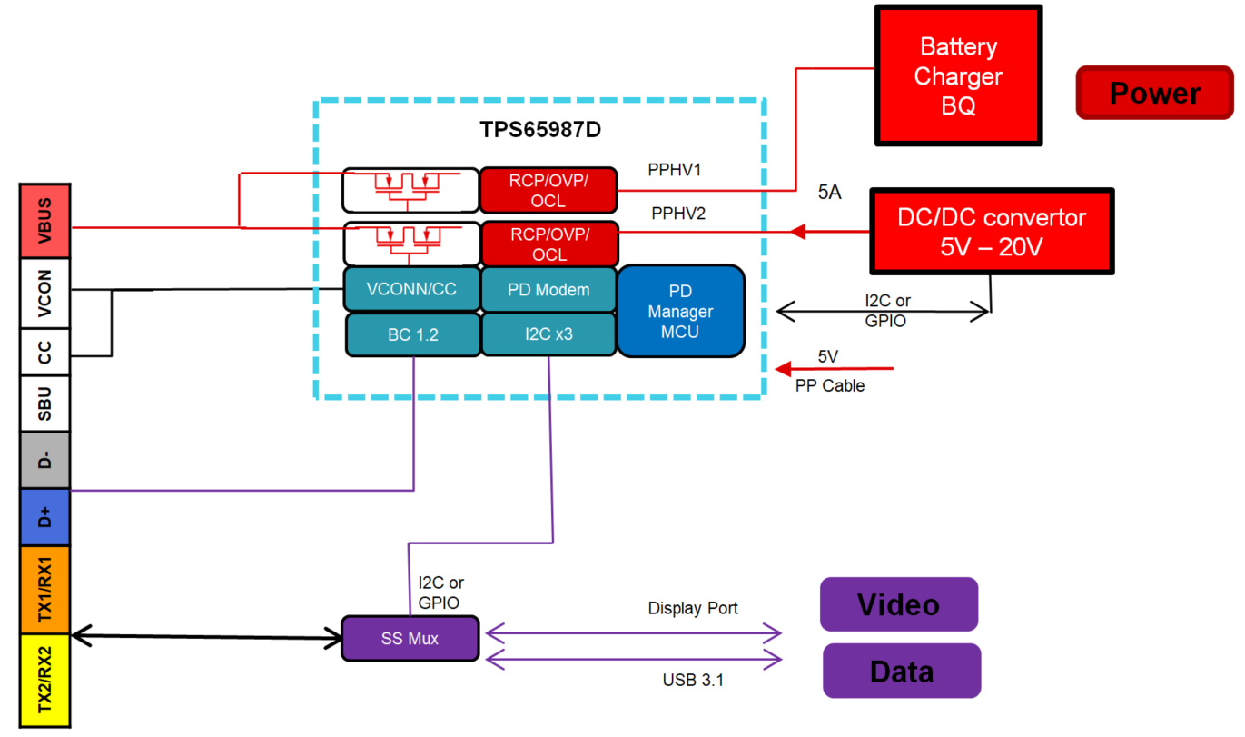
Figure 2 is a block diagram of a solution using TI’s TPS65987D. It integrates the power paths for both source and sink operation. The onboard firmware and analog circuits monitor and direct the proper operation of the power path. Simple inputs from a graphical user interface (GUI) allow you to select the voltage and current levels available and then tie in the associated general-purpose input/output (GPIO) or I2C writes needed to control external devices. See? No assembly required.

A simple-to-use GUI also facilitates USB Type-C and USB PD negotiation. Just select the USB Type-C and USB PD capabilities required and the values will be stored for uploading during device boot. Again, no assembly required.

Negotiating the USB specification and DisplayPort™ version also takes just a couple of mouse clicks to configure. Complex pin multiplexing schemes and critical timing parameters are already implemented and sent via GPIO or I2C to an external multiplexer.

Figure 2: Typical Notebook Implementation

Implementing complex USB Type-C and USB PD solutions does not need to be difficult. TI has a variety of compliant solutions with easy-to-use configuration options. Take a look at the TPS65987D evaluation module and its user’s guide to get started today.

How to eliminate interference in wireless access point equipment

$
0
0

Equipping broadband modems, routers and gateways in home and enterprise networking with wireless access point (AP) functionality is experiencing explosive growth. Figure 1 shows such a Wi-Fi® network. As the market keeps growing, the DC/DC converters used in this kind of equipment must fulfill several requirements.

Figure 1: Typical residential or small office Wi-Fi network

The first requirement is at least a 1.2MHz switching frequency. Figure 2 shows a diagram of a wireless AP. The switching noise of the DC/DC converter powering the Wi-Fi core chip will affect the error vector magnitude (EVM) of that Wi-Fi modem, thus degrading the communication quality. Fortunately, standard Wi-Fi chipset phase-locked loops (PLLs) have a frequency response that can serve as a low-pass filter with a cutoff frequency at ~1MHz.

Experiments show that it’s possible to minimize this kind of EVM interference by using a high-frequency DC/DC converter. Most wireless AP chipset manufactures, like Qualcomm and Broadcom, suggested a minimum switching frequency higher than 1.2MHz, with some margin reserved.

Figure 2: Diagram of a wireless AP

To satisfy the minimum frequency requirement, you could use a converter based on current-mode control. This kind of converter usually has an internal clock to synchronize its operation. It’s not very challenging to meet a design target such as 1.4MHz with a tolerance ±200kHz. The disadvantage is the converter’s moderate load transient performance. Sometimes, to meet the fast load transient requirements of a Wi-Fi system, you have to use a larger output capacitance, which increases the total system cost.

The second requirement is the faster load transient response. The power consumption of the amplifier in a Wi-Fi block is quite different in the data transceiver and idle states, and the state change can be very fast. This imposes higher requirements on the load transient performance of your power-supply solution.

You could choose a converter with a constant on-time (COT) mode, which is famous for its faster loop response. Unfortunately, there is no internal clock in a COT converter; the converter simply generates a proper on-time for the high-side power field-effect transistor (FET) based on the input and output voltage to maintain a pseudo-constant switching frequency. The switching frequency of a COT converter changes greatly as the input and output voltage changes. It’s very difficult to design a COT converter with a relatively tight frequency tolerance requirement.

You need a high-frequency, cost-effective solution that has fast load transient performance like a COT converter, but can also maintain a relatively constant switching frequency like a current-mode converter.

Figure 3 illustrates a proposed solution that adopts the D-CAP3™ control mode and implements a proprietary frequency-lock function to achieve a constant frequency like a current-mode device.

Figure 3: Block diagram of a D-CAP3 control-mode-based converter

Compared with the traditional COT control mode, you can realize several benefits with this solution:

  • The converter switching frequency is compared to a reference clock frequency. Based on the result, the on-time generated by a one-shot block adjusts to maintain a switching frequency within a relatively narrow variation range.
  • An error amplifier removes DC voltage errors caused by the ripple amplitude of the output voltage. This DC error normally exists in a traditional COT control-mode converter.
  • Instead of using the ripple of the output voltage as in a COT converter, a D-CAP3 control-mode-based converter will generate an internal ripple signal to emulate the inductor current ripple, eliminating the need for an equivalent series resistor on the output capacitor and achieving stable regulation even without output voltage ripple.

The frequency lock function makes it possible to achieve a relatively constant switching frequency. If the internal reference clock is set to 1.4MHz, you can easily guarantee a switching frequency higher than 1.2MHz in mass production, satisfying the first requirement. As to the second requirement, you can also meet a fast load transient response easily, since that is an inherent benefit of DCAP-3 control mode.

Let’s take TI’s TPS563249 17V, 3A buck converter as an example to obtain the measurement result.

Figure 4 shows the faster load transient response of the TPS563249 compared to a current-mode converter. To make a direct comparison, the switching frequency of the current-mode converter is set at 1.4MHz, as is the TPS563249, and the crossover frequency is set at about one-tenth the switching frequency. Both converters are using the same 1.5µH/22µF output inductor-capacitor filter.

Figure 4: The faster load transient response of the TPS563249 compared to a current-mode-based converter

The load step is from 1A to 3A with a 2.5A/µS slew rate; the target output voltage is 3.3V. The peak-to-peak output voltage ripple with the current-mode converter is 4.3% of the nominal output voltage, while it’s only 2.3% with the TPS563249.

Figures 5 and 6 show the constant switching frequency of the TPS563249 compared to a general COT converter without the frequency lock feature.

Figure 5: Frequency variation versus a different VIN (VOUT = 5V)

Figure 6: Frequency variation versus a different VIN (VOUT = 1.05V)

The TPS563249 has a smaller variation range compared to a general COT converter. As you can see, the TPS563249 also maintains a tight frequency range: there is around 5% of variation from the nominal frequency regardless of how the input and output voltage changes. However, for the general COT converter, the frequency varies ~35% from the nominal frequency in the worst case.

In general, the TPS563249 works at a constant 1.4MHz switching frequency and removes the noise interference in a Wi-Fi system for all conditions. It also satisfies the fast load change requirement from a Wi-Fi amplifier by implementing D-CAP3 control mode.

The 1.4MHz high switching frequency is helpful to minimize total system size, as well as bill-of-materials cost. It’s quite suitable for frequency-sensitive applications, such as broadband modems, routers and gateways with wireless AP.

Additional resources


Output topology options for a voltage supervisor

$
0
0

 Having stumbled upon this blog post, I’m assuming that you know the importance of having a voltage supervisor in your electronic design and are wondering how to implement and design with these different output topology types. Don’t worry! You came to the right post. But before I explain the different output topologies, I want to reiterate the importance of having a voltage supervisor, as many engineers are not familiar with this device.

Given the variable amounts of load that a system can have, the power supply is not always clean and can bounce around its typical output value. With this bounce in power supply, a device known as a voltage supervisor can provide protection from accidental surges or falling power, and improve the efficiency of electronic devices. This makes voltage supervisors a requirement in any electronic application.

The voltage supervisor products available on the market distinguish themselves by features such as threshold selections, multichannel monitoring options, detection accuracy, output configurations, fixed or adjustable delay, and watchdog features. In this post, I’ll focus on the different output configurations and review what you should consider when designing with these output topologies.

Output configurations

Think of a supervisor as an analog-to-digital converter. It senses a supply voltage (analog) and provides a flag (either the RESET or SENSEOUT pin), which is a digital signal. The digital signal output can be in either an open-drain or push-pull topology.

The open-drain output topology

Here are some things to consider when designing with the open-drain output topology:

  • Open-drain outputs provide flexibility because they can pull up to any voltage (within absolute maximum) to comply with the logic of the load, rather than pulling the output up to the supervisor’s supply voltage or sense voltage. A pull-up resistor properly limits the current and maintains the low-level output voltage (VOL) and high-level output voltage (VOH) specifications.

  • It’s possible to wire-OR together multiple open-drain outputs through a single pull-up resistor. The open-drain output can also pull up to any voltage that complies with the logic of the load giving flexibility to a designer.

  • The pull-up resistance cannot be too low such that the current through the open drain damages the supervisor. When the internal n-channel metal-oxide semiconductor (NMOS) (Figure 1) is on, current from the pull-up resistor will go through the NMOS and be pulled to ground. You should select the pull-up resistance based on two criteria. The first criteria is the supervisor’s recommended maximum reset or sense current, called IRESET or ISENSE, which is specified in the data sheet. If the current being pulled to ground is higher than IRESET, the supervisor’s internal NMOS could be damaged. The second criteria is based on the VOL requirements of the load that the output of the voltage supervisor connects to. Lower pull-up resistors will also result in higher VOL due to the increase in reset/sense current.

  • The pull-up resistance cannot be too high such that the leakage current through the open-drain resistor at high temperatures falls outside the VOH specification found in the data sheet. By increasing the pull-up resistance, VOH decreases due to the smaller reset or sense current, causing a smaller voltage drop across the internal metal-oxide semiconductor field-effect transistor (MOSFET).

  • The output rise time is decided by the pull-up resistance and the output board parasitic capacitance. For faster rise times, use smaller pull-up resistances.

  • The supervisor’s quiescent current (Iq) does not include the current through the pull-up resistor. If the pull-up voltage is pulled from the supply, the total system Iq will increase, as supply current will also go through the pull-up resistor. If the pull-up voltage connects to another source, the system Iq will equal the supervisor Iq from the data sheet. Since the pull-up voltage can connect to different supplies, the Iq specification of the supervisor does not account for the additional output current resulting from the use of a common supply.

  • An open-drain output configuration requires an additional component, a pull-up resistor, connected from the output to a power supply. Without the pull-up resistor, the outputs are undefined when the internal NMOS turns off, as there will be no power supply to pull from.

  • The open-drain output can change with the output pull-up supply, and any transient coupling will depend on the pull-up resistance used. A higher pull-up resistance can minimize the effects of transients from the output pull-up supply.

Figure 1: The open-drain output uses an internal N-MOSFET

The push-pull topology

Here are some things to consider when designing with the push-pull output topology:

  • The output of a push-pull configuration toggles between the supervisor’s supply voltage and ground, with no external pull-up resistance required. Notice how the output in Figure 2 does not use a resistor like in Figure 1, and how Vpullup is not present in Figure 2. Vdd and ground are toggled via the 2 MOSFETS.

  • The voltage at the output of a push-pull configuration can never go beyond the supervisor’s voltage supply by more than 0.3V, because the body diodes can turn on and damage the device. The body diode will take excessive current in forward bias mode.

  • The quiescent current of the supervisor accounts for the current through the external resistors that can be connected at the output of the supervisor.

  • It’s not possible to wire-OR together push-pull outputs like with the open-drain output topology.

  • Push-pull outputs are a good fit for high-speed applications because the push-pull output does not have the additional delay that the pull-up resistor causes in the open-drain topology.

Figure 2: In the push-pull output topology, a p-channel MOS (PMOS) and NMOS connect together, similar to an inverter

How to identify active low and active high

Different types of supervisors monitor under and overvoltage conditions and provide RESET/FLAG/POWERGOOD/SENSEOUT in an active-low or active-high output topology. “SENSEOUT” and “POWERGOOD” labeled pins are active when the supervisor senses the supply voltage is in normal operating condition, whereas a “RESET” labeled pin is active when the supervisor senses the supply voltage is in a fault (under- or overvoltage) condition.

An overvoltage active-high supervisor means that whenever the supply crosses VIT+, signaling an overvoltage condition, RESET activates to logic high.

Table 1 can help you identify the different supervisors.

Table 1: Active-high vs. Active-low supervisors.

Now that you know more about the different output topologies, you are one step closer to selecting the correct supervisor for your system. Check out TI’s quick search tool to help you find one.

Additional resources

How to Create a Programmable Output Inverting Buck-Boost Regulator

$
0
0

By Akshay Mehta and Frank De Stasi

There are multiple applications, particularly in the test and measurement sector, where you need an external source or digital-to-analog converter (DAC) to program the output voltage of an inverting buck-boost regulator. To do that on a regular buck topology is fairly straightforward: all you have to do is inject current into the feedback node, using a voltage source with a series resistor, a current source or even a DAC, as shown in Figure 1.

1. Programmable voltage with a buck topology.

But when you have to change the voltage of a regulator operating in the buck-boost topology, things start to get a little tricky.

You can configure a buck regulator in the buck-boost topology simply by reversing the ground and VOUT potentials and having the reference of the integrated circuit (IC) now be at the -VOUT potential. This means that the ground pin of the regulator IC is at -VOUT. The FB pin of the regulator is sitting over the -VOUT potential and not the ground potential, and this makes injecting current into the FB pin a tad difficult. To inject current into the FB pin in an inverting buck-boost topology, you’ll need to level-shift the signal from the voltage source/DAC. So in this article, I’ll show you a few different approaches how.

Let’s use the LMZM33606 from Texas Instruments as an example throughout. The LMZM33606 is a buck power module rated for 36V at the input and can supply a max load of 6A. Figure 2 shows how to set up the LMZM33606 as an inverting buck-boost regulator.

2. Inverting buck-boost with the LMZM33606.

Approach No. 1: Level Shifter with a Single PNP

Using the LMZM33606 in these buck-boost applications, it’s possible to demonstrate a programmable output voltage range of -15V to -5V. With the current-source approach, you can reduce the output of the regulator in absolute magnitude. This means that you can set the feedback divider resistors such that the default output of the design is -15V. When adding an external current source, you can then program the output of the regulator to -5V. For the default of -15V, calculate the upper and lower feedback values as:

  • RFBT = 100kΩ.
  • RFBB = 7.42kΩ.

The simplest way to level shift a ground-referenced signal to inject current into the FB pin is to use a single p-channel n-channel p-channel (PNP)-type bipolar junction transistor (BJT). Figure 3 shows how a single PNP can be used as a level shifter.

3. Implementation using a single PNP.

The PNP Q1 has its base grounded and the emitter connects to the DAC/voltage source through a resistor. When the voltage source level increases above the base to emitter voltage (VBE) drop of the PNP, there will be current flow governed by Equation 1:


Rext is set at 50kΩ. Applying Kirchhoff’s current law at the FB node, you can calculate this current IX with Equation 2:


By substituting equation 1 in equation 2, we obtain equation 3 which finds the value of the programming voltage VX required to change the output voltage, VOUT:


Turning Equation 3 around to Equation 4 gives you the VOUT that you can program based on the value of VX:


Equation 4 denotes the dependence of VOUT on the VBE of the transistor. The VBE of the transistor is itself dependent on the collector current, which when changed with temperature will result in some inaccuracies in the programmed VOUT.

The next approach shows how to remove VBE from the equation. Figure 4 shows a circuit with two PNP transistors that are connected such that the effect of VBE can be nullified.

Approach No. 2: Level Shifter with Two PNPs

4. Implementation with two PNPs to nullify VBE.

This approach requires an additional PNP – ideally you should use two co-packaged PNP BJTs to ensure good matching between the two transistors. This approach will reduce errors in the programming of the output voltage.

The Q1 transistor has its base connected to the programming voltage source. The emitter then connects to another positive rail through a series resistor RS and the collector is grounded. This creates a voltage of VX + VBE at the emitter of the transistor. The Q2 transistor’s emitter connects to Q1’s emitter through resistor RX. RX sets the current to be injected into the FB node. With the base grounded, there is a +VBE generated at the emitter node of Q2. Equation 5 calculates the current flowing into the emitter (ideally) as:


From earlier, you know that the VBE of the transistor will depend on the collector current, expressed as Equation 6:


where IC is the collector current, IS is the saturation current and VT is the thermal voltage.

If the collector currents of the two transistors are very different, then the VBEs do not completely cancel each other out. Equation 7 expresses the difference in the two VBEs of the transistors as:


Simplified to Equation 8:


where X is the ratio of the two collector currents.

As you can see, if the two collector currents are equal, the VBEs will cancel out completely. In the configuration shown in Figure 4, it will be important to size the value of RS such that the difference in the collector currents is not considerable. For this example, I chose an RS of 10kΩ and an RX of 50kΩ. The delta in VBE will also change with the change in VT, which happens with changes in temperature.


Approach No. 3: A Modified Wilson Current Mirror

A good way to match collector currents is to use a current mirror. But there is one option better than a regular current mirror, and that is the Wilson current mirror. Figure 5 shows the schematic used for the Wilson current mirror.

5. Implementation using a Wilson Current Mirror.

In this approach, there is an additional BJT with its base connected to the collector of Q1. The emitter of Q3 connects to the VBE junction of the mirror. The programmed current flows through the collector of the Q3 transistor into the FB pin.

Ignoring resistor RB for now, Equation 9 calculates the reference current being injected in this setup as:


Equation 10 derives the ratio of injected current to reference current in this setup as:


Given the betas () of the transistors in high values, you can see that the Wilson current mirror gives you a lot more accuracy than the standard current mirror.

The Wilson current mirror doesn’t completely eliminate the dependence on VBE. But there is a pretty simple trick to get around this. Connecting a resistor RB from the source VX to the base of the mirror, as shown in Figure 5, creates a current flow that gets added to reference current IX. Rewriting Equation 9as Equation 11:


Equation 12 chooses RB such that:


Then Equation 13 is:


The VBE component in Equation 13 cancels out completely, resulting in Equation 14:


Equation 14 shows that the current injected into the FB node is based just on the programming voltage and has no dependencies on VBE.

Using any of these approaches can help generate a programmable output voltage for an inverting rail with just a few extra components. The circuit complexity will vary based on the system requirements. For applications that require very high fidelity, the Wilson current mirror is the best solution, as it gets the closest response to the programming voltage.

References

LMZM33606 data sheet

Toumazou, C., F.J. Lidgey and D.G. Haigh (Ed.), “Analogue IC Design: The Current-Mode Approach,” London: Peter Peregrinus Ltd., 1990.

Delivering a smooth transition from AC to PoE power

$
0
0

As the number of interconnected devices in the electronics market continues to grow, it becomes increasingly important to ensure interconnectivity between data-sensitive end equipment like wireless access points (WAPs), Internet Protocol (IP) cameras and security systems. Otherwise, data loss could occur, resulting in the loss of valuable information such as surveillance data. For data-sensitive applications like these, TI is here to help guide you on how to minimize the risk of data loss for Power over Ethernet (PoE) applications.
One method of decreasing the probability of data loss in a PoE system is to implement hitless failover, which enables the transition from main power to backup power without a loss of power at the load (in other words, the load does not reboot/restart and continues in normal operation). Hitless failover helps ensure continuity of service, lowering the probability of power loss and data outages.

Let’s walk through an example to see how you can implement hitless failover with the Dual-Input Redundant PoE PD with Smooth Transition Reference Design and a WAP like the one shown in Figure 1 with dual PoE inputs and a single AC/DC wall adapter input.

Figure 1: WAP with dual PoE and single AC/DC adapter inputs

In this example, the goal is to avoid data loss at all costs. Implementing three power supplies (two DC/DC PoE supplies and one AC/DC wall adapter supply) decreases the probability of power (and thus data) loss. In the event that the primary power source is unavailable due to harsh conditions, accidental trips or cable damage, one of the secondary power sources quickly transitions to become the main power source without dropping the output voltage at the load.

To implement hitless failover, you will need to choose a PoE PD device that has the automatic maintain power signature (MPS) and inrush delay features integrated – devices like TI’s TPS2372 or TPS2373 Institute of Electrical and Electronics Engineers (IEEE) 802.3bt PoE PDs, which can power loads up to 71W. The auto MPS feature is an electrical signature presented by the PD to assure the PSE that it is still present after applying the operating voltage. This automatically generated signature allows the PD to remain connected to the power sourcing equipment (PSE) and in active standby mode in the event that the main power supply goes down.

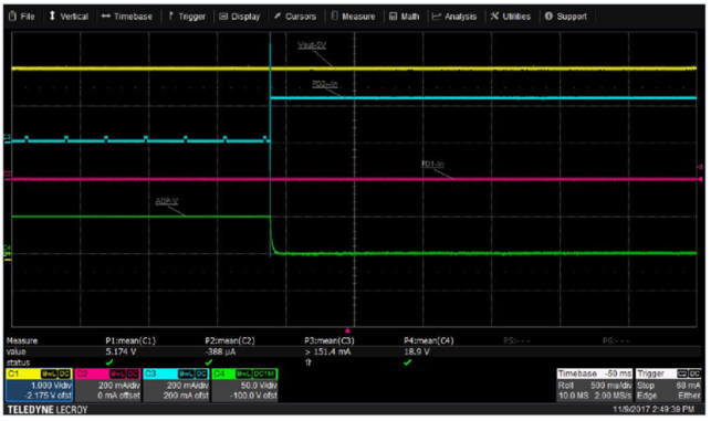
Now, let’s take a look at the hitless failover power transition as shown on the oscilloscope. In the reference design the adapter has power-supply priority over PoE1 and PoE2. Now, imagine that the adapter supply fails.

As shown in Figure 2, the output voltage of the AC/DC adapter (green) suddenly drops to zero while the output voltage of the secondary power source PoE2 (blue) transitions to being the main power source. During this transition, the input voltage to the WAP (yellow) remains constant at 5V. This enables the load to remain powered and for data to transmit continuously, even during the transition between power supplies.

Figure 2: Adapter and PoE power transition with hitless failover

Hitless failover power transition has become increasingly important due to the need for data-sensitive end equipment to avoid the loss of data transmission. If you are interested in enabling hitless failover in your PoE PD design, consider using a device with auto MPS and in-rush delay integrated such as TI’s TPS2372 or TPS2373 and the reference design I described here.

Additional resources

How to speed SSD program time with a boost converter

$
0
0

Solid-state drive (SSD) storage is becoming more popular in PC, data-center and telecom applications, offering the benefits of faster speeds and a more compact size compared to Hard Disk Drive (HDDs). The new Peripheral Component Interconnect Express (PCIe) Non-Volatile Memory Express (NVMe) Host Controller Interface Specification SSD offers three times faster write speeds and six times faster read speeds compared to traditional Serial Advanced Technology Attachment (SATA) SSDs.


However, increasing Not-AND (NAND) flash write and erase speeds, as well as solving the thermal dissipation, impose big challenges on SSD designs.


A power supply is required to support the write/erase of the NAND chip, as shown in Figure 1.


Figure 1: Write/erase the NAND flash cell


Equation 1 calculates the current during write/erase as:


I = C * (dVs / dt) + (Vs / R)                             (1)


For instance, if C is around 100 pF, R is around 1 MΩ. If write/erase completes in 100 ns, the current is around 12 mA. For an application like enterprise storage, a larger capacitance (increasing C) and faster speeds (decreasing t) require a higher current. The write/erase speed really depends on the power-supply capability and the overall thermal dissipation. If the power capability cannot deliver the required current due to current capability, the write/erase speed will scale down which in return impacts the response time of the storage system.

Charge-pump converters vs. inductive boost converters

There are two basic types of step-up converters: a charge-pump converter and an inductive boost converter. Since charge-pump converters don’t use an inductor, the solution area for a charge-pump converter is relatively smaller and could be put into a NAND cell, as shown in in Figure 2.


Figure 2: Traditional NAND flash chips with an in-cell charge-pump converter


The charge pump solution for applications with higher output-power requirements needs a larger capacitance due to charging/discharging capacitance with heavier load. The efficiency at heavy loads is also relatively low due to the power loss of the charging/discharging capacitor. Additionally, there are high output ripples and noise as well at heavier load conditions. Based on the limits of lower current capability, the charge-pump converter is a good fit for relatively lower-power applications, while being easy to design (since there is no inductor) and having a small solution size with medium-level efficiency.


In contrast, an inductive boost converter can deliver more current than a charge-pump converter and will have lower ripple, which makes it a more competitive solution for higher-power applications. The output voltage of the boost converter could be flatter across the whole load range as the inductor current could deliver the load current. As shown in Figure 3, placing a single boost converter outside of NAND chips could supply the power of multiple chips.


Figure 3: NAND flash chips with an inductive boost converter

The TPS61372 synchronous boost converter could be a good fit for supplying the power to write/erase NAND chips in SSDs. It has a compact solution size and minimizes the need for external components. Compared to traditional charge-pump converters, the TPS61372 can deliver a higher-quality power supply to write/erase NAND chips.


Additional resources

20 million reasons to use GaN

$
0
0

It was a cold and snowy day in Toronto.

We were brainstorming in the basement of the local university’s advanced power electronics research lab. Ironically, the conversation was focused on heat – not actually generating it for warmth, but how to reduce it in our power converters. We had pushed MOSFETs and IGBTs to their respective limits, yet none of us were satisfied. Throughout the process, we had accumulated a stack of devices that had failed in our high-stress environment.

On that snowy day, we chose to focus on finding new ways and topologies to get to higher levels of efficiency and density, and of course ways to improve robustness. One of the senior researchers helped summarize our challenge: “We can do all of these ideas. But first, give me the perfect power switch.” The statement was mixed with frustration and hope.

Years later the perfect power switch arrived. In 2018, we released to production our family of 600-V gallium nitride (GaN) FETs with an integrated driver and protection, including the LMG3410R070, LMG3411R070 and LMG3410R050. Each device is capable of megahertz switching and delivering multikilowatt power levels – enabling smaller yet more efficient designs not previously possible.

Before release, TI invested heavily in device robustness for use in every power application to give designers the confidence they need to use GaN, accumulating 20 million hours of device reliability testing in the process.

The “perfect power switch” has arrived

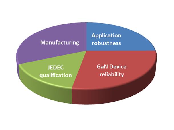
TI has always been on the forefront in advocating for the development and implementation of a comprehensive methodology to ensure the reliable operation and lifetime of GaN devices under the harshest operating conditions. To achieve this, we extended the traditional silicon methodology for GaN and its intrinsic characteristics. Additionally, stress testing needed to include the hard-switching conditions common in switch-mode power supplies, which traditional silicon qualification does not address. TI focused its testing in four categories:

  • Device reliability: Pertains to how the device is engineered; establishes the intrinsic lifetime of the device.
  • Application robustness: incorporates mission-profile conditions under acceleration to emulate realistic use conditions.
  • Manufacturing: focuses on production flow optimization and yield improvement.
  • Joint Electron Device Engineering Council (JEDEC) qualification: the quality of the device and its ability to survive accelerated test conditions to predict low defective and failure rates.

 20 million device reliability hours and counting

Additionally, the power electronics industry reached an exciting milestone in 2017. JEDEC announced the formation of JC-70.1 to standardize reliability and qualification procedures, data-sheet elements and parameters, and test and characterization methods for GaN. As a founding and active member of JC-70.1, we at TI are committed to helping the industry further apply the benefits of our methodology, expertise and know-how, building on our 20 million hours of device reliability testing.

The perfect power switch is no longer a fantasy in a cold basement. It’s a reality, and enabling designers to do what they do best: push the envelope to power densities and efficiencies never seen before.

Additional resources

How to add hysteresis to a DC/DC converter

$
0
0

Is enable hysteresis not included in the DC/DC converter you are designing with? Or is the built-in enable hysteresis too small?

Modern DC/DC converters use an enable pin to control the design conditions at which the power supply turns on and off. It is possible, however, to add an adjustable hysteresis to your DC/DC converter’s enable signal. You can replicate this technique using Excel spreadsheet calculations, Texas Instruments (TI) TINA-TI™ software simulations and evaluation module (EVM) testing.

It is standard electrical engineering practice to add a hysteresis resistor around a comparator (adding feedback). You can apply this same idea to a DC/DC converter by adding a resistor connecting the enable signal to the output voltage. By adding the output voltage to the enable signal, the enable signal will be pulled even higher once the converter produces an output. Figure 1 shows a simplified schematic.

Figure 1: Simplified DC/DC Converter Schematic

You can use Equations 1 through 4 to calculate the correct resistor values based on the design parameters:

where RT is the top feedback resistor in the enable resistor network, RB is the bottom feedback resistor in the enable resistor network, VON is the desired input voltage for turnon, VOFF is the desired input voltage for turnoff, RHYS is the hysteresis resistor, IDRAW is the current drawn by the enable resistor network and VEN is the enable threshold voltage (a data-sheet specification).

Example

In this example, the converter will be enabled once the input voltage reaches 10V. Once on, the input voltage will decrease down to 7.5V before the converter becomes disabled. This means designing a system hysteresis of 2.5V into the enable signal. The specific design parameters are:

  • VIN typical = 12V.
  • VON = 10V.
  • VOFF = 7.5V.
  • VOUT = 5V.
  • VEN = 1.2V (no internal hysteresis).

Now let’s look at the calculations, simulations and test data for this additional hysteresis.

Step 1: Use the design calculator to determine resistor values

The Excel design calculator can calculate the resistor values corresponding to your desired design parameters. In the yellow boxes (Table 1), enter the preferred turnon voltage, the amount of added hysteresis, the VEN threshold, the total desired current draw and the output voltage. Use the enable resistor network current draw entry to select how much current you will budget for the enable network. By selecting a smaller value, the resistor magnitudes will increase. Enter this value in microamperes.

Table 1: Example using Excel design calculator

The Excel calculator quickly recommends the appropriate component values for the desired VON and VOFF. Table 1 also shows the calculated RT, RB and RHYS values to meet the input criteria.

Step 2: Simulate the values using TINA-TI software

You can use a TINA-TI simulation in order to simulate turnon and turnoff performance with the calculated resistor values. Adjust RT, RB, RHYS, VEN and VOUT amplitude to match your design calculations. Figure 2 shows the TINA-TI Simulation schematic that can be adjusted to test out different values.

Figure 2: TINA-TI Simulation Schematic

Click Analysis and then Transient Analysis to run the simulation. Running from 750ms to 1.75s will show a full turnon, turnoff cycle. Figure 3 shows the simulation results.


Figure 3: TINA-TI Simulation Transient Results

Step 3: Validate on an EVM

Wiring in the hysteresis resistor to a TI EVM will allow you to test in the lab. For this example, I used the TI LM73605 EVM with a small resistive load and a signal generator to provide the input ramp waveform. Figure 4 demonstrates the physical implementation of the hysteresis example with results measured on an oscilloscope.

Figure 4: EVM Testing Results

Conclusion

The Excel calculator allows for quick design of a hysteresis network. The simulation files prove the mathematical validity, showing the same turnon and turnoff threshold as the calculator. Finally, testing in the lab proves that at the applications level, the turnon and turnoff thresholds are very close to the ideal, corresponding to the calculator. The Excel calculator, simulation tools and EVM testing provide a quick and accurate method to add hysteresis to your DC/DC converter.

For your next DC/DC power design, download the enable hysteresis Excel calculator and enable hysteresis TINA-TI simulation to help fast-track your added power-stage hysteresis.

QFN soldering tips and tricks

$
0
0

 If you’re looking to power a space-constrained, high-power-density, thermally critical application, high-efficiency converters in tiny quad flat no-lead (QFN) packages offer great performance value. But you might ask yourself, when you test and debug your prototype boards, will you be able to handle those minuscule packages in your lab? Will you need special equipment or soldering talent?

No need to worry – it’s much easier than you think! Our lab experts have some hands-on tips and tricks for you.

First, make sure that your board is completely dry – otherwise there’s a risk of printed circuit board (PCB) delamination. Uniformly heat up the board from the bottom using a ceramic hot plate set at ~150°C (you can safely go up to 200°C for larger PCBs with eight layers or more).

To reach the right local soldering temperature, point a hot-air nozzle toward the integrated circuit (IC) landing position on the PCB. Since the IC package temperature should not exceed 260°C per TI specifications, be careful to limit the hot-air temperature.

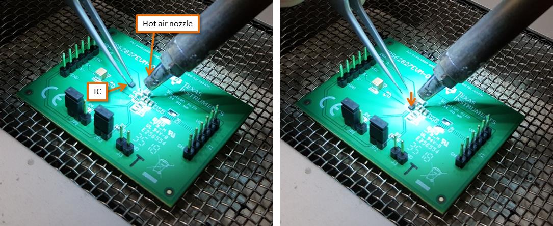
Once you’ve reached a stable temperature, apply the flux and distribute the solder evenly on the PCB pads (for such small packages, we use lead-free, 0.2-mm solder wire). Hold the IC with tweezers a few millimeters away from the landing pads during the PCB pad pre-tinning process. When the solder is molten on the pads, stop the airflow and drop the IC on the PCB pads (see Figure 1). The IC will self-align to the PCB pads as long as the solder is liquid. Carefully blowing some hot air again will help support the alignment.

Figure 1: Keeping the IC above the landing pads during the pre-tinning process (a); dropping the IC on the PCB pads once the solder is molten and carefully blowing hot air to support the alignment (b)

Try to work as quickly as possible to avoid using up the flux and having the solder oxidize before you’ve properly placed the IC. Of course, pay attention to elementary precautions like working in an electrostatic discharge-safe environment.

That’s it!

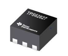
When you start working on your next thermally critical design using our new TPS62827, a 2- to 4-A high-efficiency buck converter in a 1.5-mm-by-1.5-mm QFN package, also check out the data sheet, which has specific guidance on how to properly lay out the PCB land pattern, solder mask and solder stencil for this package. In addition, the application note “QFN and SON PCB Attachment” gives a detailed overview of the essentials for ensuring the smooth manufacturability of your board.


Using an RGBW LED driver to elevate LED human-machine interface designs

$
0
0

Smart Home Connected IoT

Products are becoming very intelligent and connected with each other. Devices such as speakers, TVs, refrigerators, set-top boxes and smoke detectors are no longer objects that just sit there – users can control them remotely or through voice wakeup. Devices are much smarter than before, which means they will also require an improved human-machine interface.

A light-emitting diode (LED) indicator like an LED ring, LED matrix or red-green-blue (RGB) LED lighting interacts with users by changing patterns, such as chasing or blinking. Figure 1 shows some pattern examples.

Personal Electronics  RGB LED White LED Drivers  Power Button Control


Figure 1: Examples of LEDs used for a human machine interface

To have a very friendly human-machine interface, these elements are important:

  • Perfect color mixing, with the color changing at the user’s request.
  • Smooth LED brightness: not too dark during the day and not too bright at night.
  • Nice dynamic changing effects, like chasing or blinking.
  • Power efficient in case the power comes from a battery.

While at first this list may seem daunting, all you need to generate great LED effects is a smart LED driver with these key features:

  • The ability to drive multiple channels with a proper communication protocol like I2C. A microcontroller (MCU) could talk to this device and control each channel independently, without consuming a lot of general-purpose input/output.
  • High-resolution pulse-width modulation (PWM) control for changing the brightness of the LEDs.
  • A very low quiescent current, as well as a proper power-saving mode.
  • High-frequency pulse-width modulation to avoid audible noise, since many LED indicators are used with speakers.

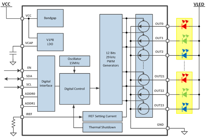
TI’s LP50xx family of multichannel, RGB LED drivers, shown in Figure 2, is a good fit with this feature list.

TI LP50xx Family Functional Block Diagram

Figure 2: LP50xx family functional block

The devices integrate a 12-bit PWM generator that operates above a human-audible frequency, at 29 kHz per channel, enabling smooth, vivid color with zero audible noise. 18-, 24-, 30- and 36-channel options provide independent color mixing and brightness control. With an integrated power-saving mode, these LED drivers dramatically reduce power consumption to improve total system efficiency in standby mode.

The LP50xx family enables you to achieve seamless, smooth animation in applications that use a human-machine interface, such as portable electronics, building automation and appliances.

Additional resources

How to use a voltage reference as a voltage regulator

$
0
0

A version of this post was also published on Electronic Design.

Have you ever needed to bias a low-current load and simply didn’t want to add another voltage regulator? Or been in a situation where you need a reasonable level of voltage accuracy, so a simple voltage divider isn’t enough?

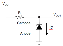
For many years, designers used Zener diodes as a simple shunt voltage regulator, as shown in Figure 1. With a single resistor, the device will maintain the fixed voltage determined during the manufacturing process.

Figure 1: A single resistor and Zener diode create a simple voltage rail

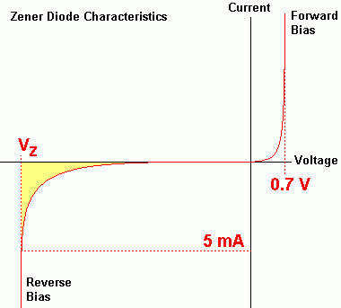
A good Zener diode works well, but when you look closely at the data sheet, you’ll see that you need to source more than a few milliamps in order to realize an accurate Zener voltage (Vz). To maintain accuracy, you must choose a low-enough series resistor value to ensure that the Zener reverse bias current (Iz) falls within an acceptable range. As shown in Figure 2, this range may be as high as 5mA, especially with lower-cost, non-temperature-compensated diodes.

Figure 2: Zener diodes typically require a more than a few milliamps to reach Vz

Ohm’s law and Joule’s law dictate the power losses across the shunt resistor, which affects overall system losses and temperatures. As an example, with a 12V input, using a 2.5V Zener diode would require a 1.9kΩ series resistor in order to maintain 5mA (assuming no load current). A 1.9kΩ resistor with 5mA results in a loss of over 47mW across the resistor. With 24V, the losses are over 100mW.

A voltage reference (also called a band-gap reference) provides the same functionality as a Zener diode yet requires far less current to maintain a more accurate voltage. Where a Zener diode uses a single p-n junction with specific doping to create a Zener breakdown voltage, a voltage reference uses a combination of transistors and employs a positive-temperature-coefficient p-n junction in concert with negative-temperature-coefficient transistors to make a zero-temperature-coefficient reference.

The concept and design of a band-gap reference was introduced back in the 1970s by Bob Widlar when he was a power integrated circuit (IC) designer. Although voltage references are often employed because of their voltage accuracy (well under 1%) over temperature and time, advances in semiconductor circuitry, processes and packaging have brought them into new applications.

Wider-tolerance and lower-cost voltage references (1% and 2%) open up their use in applications where they were never before considered, applications where you might be using a Zener diode or voltage regulator. Using a voltage reference in place of a Zener diode is about efficiency and simplicity.

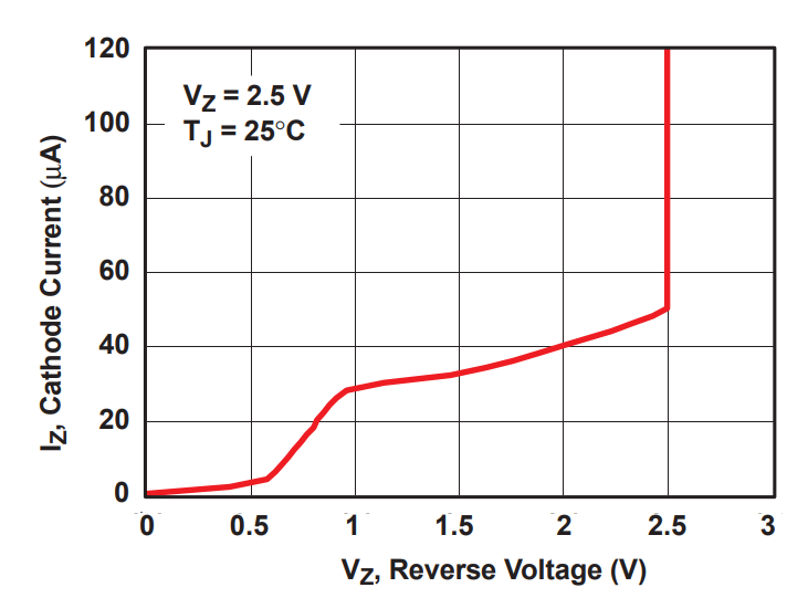
As shown in Figure 3, the voltage across the voltage reference becomes well regulated when Iz is only 50µA. Figure 3 shows characteristics of the Texas Instruments (TI) LM4040 at 25°C, yet the data sheet shows superb voltage accuracy when biasing well below 100µA over ambient temperatures from -40°C to +125°C (this is the extended Q-grade temperature version; the normal industrial temperature range is -40°C to +85°C). Some voltage references operate at an even lower current, such as the ATL431 and LM385.

Figure 3: The TI LM4040 2.5V voltage reference

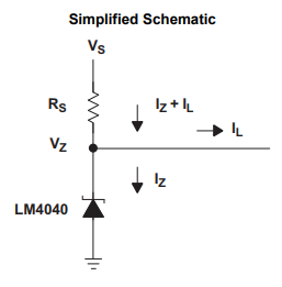
Using the same 12V example as above, with 75µA for Iz instead of 5mA, you can use a 126kΩ resistor and maintain a more accurate voltage. Using a 126kΩ resistor also enables you to realize a power loss in the resistor under 1mW, which is well below the 47mW loss when using a Zener diode. Of course, when delivering current to a load, you will need to select a lower-value resistor in order to deliver load current while maintaining the needed Iz for regulation over load variations. As shown in Figure 4, simply calculate the current through the shunt resistor (Rs) where Ir = Iz + Iload and then size the shunt resistor (Rs) using Ohm’s law, R = (Vs-Vz)/Ir. Be sure to use the worst-case load current and take tolerances into account when selecting this resistor.

Figure 4: Calculate Rs to accommodate the worst-case load current while maintaining the minimum Iz

By using a wide-tolerance voltage reference like the 2% LM4040E from TI, you can realize a regulation voltage superior to most voltage regulators at a price lower than a typical voltage regulator and on par with a Zener diode. These devices are also available in small SC70 packages. An advantage of using a voltage reference for voltage-regulation applications is their ability to operate over very large voltage ranges; a voltage reference doesn’t care about voltage, only current. By choosing the right shunt resistor value based on the input voltage range and output current, you can support a very wide range with a simple solution.

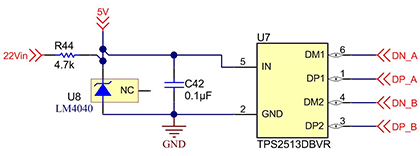
Figure 5 is an example of using the LM4040 to develop a low-current 5V rail from a 22-25V input to bias the 5V input to a USB controller IC, which only needs 100µA worst case. The resistor value selected takes into account additional bias current for a load not shown. This application can use the lower-cost 2% E version of the LM4040-N device. As you can see, the circuit is very simple and small when using 0402 passives.

Figure 5: LM4040 voltage reference used to develop 5V

Because you need higher current, the shunt resistor will need to be larger in order to dissipate the thermal losses caused by the voltage drop. The maximum current through most voltage references is in the order of 10mA to 30mA, which limits applications.

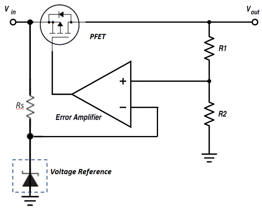
For higher current, you can employ the same voltage reference with a bias resistor along with an additional transistor to provide the necessary input-to-output voltage drop. A p-channel FET transistor biased directly from a voltage reference can supply much higher current, yet the output voltage (Vout) will vary with load current as a function of the FET’s RDS(on) characteristics. By adding an error amplifier (a single rail-to-rail operational amplifier works well), the circuit shown in Figure 6 senses Vout and compares it to the voltage reference to provide a well-regulated voltage over various changes in load current and temperature.

Figure 6: A voltage reference is at the heart of all voltage regulator circuits

Removing R2 (and shorting R1), the circuit shown in Figure 6 will provide a very well-regulated voltage equal to the voltage of the voltage reference. Voltage dividers R1 and R2 provide a means to adjust the output to any voltage greater than or equal to the reference voltage.

A voltage reference is at the heart of almost all integrated voltage regulators. You might ask, if it’s this easy, why use an integrated voltage regulator at all? One reason is that a voltage regulator also includes circuitry to monitor and limit current to the load, and monitors the temperature to protect the device and load during fault conditions. Although designers can and do design discrete voltage reference-based regulators, it’s often more practical and cost-effective to use one of the many integrated voltage regulators available today.

So the next time you need a low-current rail voltage, consider using a voltage reference.

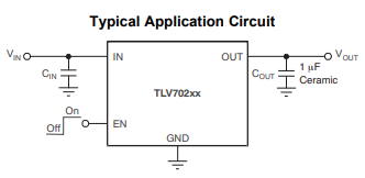
Incidentally, significant technical advancements have also been made with both linear and switch mode voltage regulators. When trying to develop a low current voltage off of a 5V rail (or higher) Texas Instruments has recently released a broad family of cost optimized and small solution size linear regulators. The new TLV702 regulator seen in Figure 7, supports up to 5.5V input and offers a wide range of voltage options, a shutdown pin, and the family is available in very small packages.

Figure 7: The TLV70 regulator family provides another cost effective alternate to Zener based shunt regulators

From a switch mode regulator standpoint, the industry has also seen significant advances in both low current as well as high current regulator solutions. Much advancement has taken place with self-contained switcher modules which include all of the necessary magnetics and are very handy for creating low voltage rails. These small modules also have the advantage of lower EMI than traditional discrete solutions, mostly based on lower impedance connections between the self-contained high speed switching nodes. Recently they have become very popular for local rail generation based on their ease of use and decreasing cost based on economy of scale.

The TPS8208x buck regulator family is very small (3.0mm X 2.8mm) and produces tightly regulated voltages with output current up to 3A. For input voltages up to 36VDC, consider the LMZM23601. This small 3.8mm X 3.0mm module can produce low voltage rails with currents up to 1A and higher current versions are available.

Choosing the best power regulation solution for a specific application always takes time and effort, and today more solutions than ever are available. Here we described some obvious and some not so obvious design options, each with specific subtle but often critical advantages that vary greatly depending on system application.

Additional resources:


Improving data-center efficiency with eFuses

$
0
0

According to Forbes, global data centers used approximately 416TW (4.16 × 10¹⁴W) of electricity in 2017, with U.S. data centers contributing about 90 billion kilowatt hours to that number. With artificial intelligence making strides and 5G around the corner, this level of power consumption isn’t declining anytime soon. Power doesn’t come cheap, and increasing financial, technical and even political factors are driving the data-center market to pursue more and more efficient engineering solutions.

One way to conserve power is to monitor how much power each server consumes. If a server is consuming too much power, it isn’t maximizing its workload per unit of power consumed. For example, if two servers in a data center are operating comfortably but server No. 3 is drawing significantly more power because it has a higher workload, the whole system is operating inefficiently. To remedy this, a central power-management system can allocate part of server No. 3’s workload to server Nos. 1 and 2 to optimize workload sharing. As a result, overall power consumption will drop because all of the servers are operating efficiently – see Figure 1.

 overall system efficiency increase

Figure 1: Reallocating the workload increases overall system efficiency

For this process to work well, however, the servers must accurately present how much current they are consuming so that the power-management system can determine if any changes need to be made. TI designed the TPS25982 eFuse to provide this accuracy and efficiency. The 15A, TPS25982 eFuse integrates a 3mΩ hot-swap metal-oxide semiconductor field-effect transistor (MOSFET) to protect against overcurrent and overvoltage conditions, while simultaneously providing both accurate current monitoring and board space savings, as seen in Figure 2.

Protection and current monitoring

Figure 2: The TPS25982 eFuse provides protection and current monitoring

Integrating all monitoring circuitry inside the eFuse eliminates the need for large external sense resistors, which saves size and minimizes voltage loss. And since accuracy is so crucial, the TPS25982 analog current monitoring feature IMON has an accuracy of ±1% typical and ±3% maximum across the entire operating current and temperature range, enabling power-management circuitry to receive the most precise information from the servers. Figure 3 below demonstrates the IMON accuracy for different currents.

Figure 3: TPS25982 monitoring accuracy at various currents

As the world’s fossil fuel resources decline, data-center computing capabilities and power consumption continue to climb. And although this advancement brings exciting new possibilities, the need for energy efficiency has never been more apparent. Take a look at the TPS25982 eFuse to see how you can optimize your system today.

Gallium nitride: supporting applications from watts to kilowatts

$
0
0

Two years ago, TI announced its first 600-V gallium nitride (GaN) power device, which paved the way for engineers not only in power density and efficiency capability but also ease of design, with an integrated gate drive and robust device protection. Since then, we’ve worked to push the power levels as high (and as low) as possible with this cutting-edge technology.

GaN is pivotal at any power level where engineers are striving to increase switching speed, efficiency and reliability while decreasing size, weight and component count. Historically, you’ve had to trade off at least a few of these, but TI is enabling designs with all of these benefits, while saving system-level costs and board component count through sophisticated integration in one package. From cutting the size of your PC adapter in half to creating highly efficient and compact 10-kW conversions for grid-tied applications, TI offers a GaN solution for your design. The LMG3410 and LMG3411 families are rated at 600 V, and offer a variety of solutions from low-power adapters to over 2-kW designs.

Device selection by on-state resistance

Internal GaN field-effect transistors (FETs) are rated by RDS(on)– the drain-to-source, or on-state resistance – which plays a big role in the switching and conduction losses in power converters. These losses affect system-level efficiency and thermal and cooling methods. So in general, the lower the RDS(on) rating, the higher level of power achievable while still maintaining high efficiency. But there are some applications or topologies in which a higher RDS(on) may be more appropriate as shown in figure 1.

Figure 1: 70- and 50-mΩ GaN devices in typical power topologies

Overcurrent protection

Integrated overcurrent protection not only eases layout and design for users, but high-speed detection is actually very necessary for device protection in case of a short circuit or other fault conditions. TI’s portfolio of GaN devices has <100-ns current response time to self-protect against unintended shoot-through events by safely shutting off the device and allowing it to reset. This protects both the device and the system from fault conditions read out from the fault pin as seen in Figure 2.

 Figure 2: Internal device structure for the LMG3410/LMG3411 families, including FET, internal gate drive, slew-rate control and protection features

TI’s default overcurrent protection method is classified as “current-latched” protection; meaning that, if any overcurrent fault is detected in the device, the FET will safely shut off and remain off until the fault resets. In our 70-mΩ devices, the fault is triggered at 36 A; for 50-mΩ devices, the fault trigger is extended to 61 A.

Depending on the application, some engineers may prefer to operate through reasonable transient conditions, for which we offer cycle-by-cycle overcurrent protection. With cycle-by-cycle protection, in the event of an overcurrent fault, the FET will safely shut off and the output fault signal will clear after the input pulse-width modulator goes low. The FET can turn back on during the next cycle and operate through transient conditions while still preventing the device from overheating.

Table 1 shows TI’s various GaN devices by their key specifications, structure and typical system power levels.

Device

Voltage (V)

RDS(on) (mΩ)

FET configuration

Overcurrent protection method

LMG5200

80

15

Half bridge

External

LMG3410R050

600

50

Single channel

Latched

LMG3410R070

600

70

Single channel

Latched

LMG3411R070

600

70

Single channel

Cycle-by-cycle

Table 1: GaN selection by key parameters

There is no doubt that GaN is at the leading edge of the semiconductor race for a superior power switch. With TI’s GaN devices now in mass production and targeting a wider range of solutions, we’re continuing to make it a more scalable and accessible technology for everyone in the power industry.

Additional resources

Big things for power come in small packages

$
0
0

Semiconductor packaging includes much more than just the material encapsulating the chip. While containing critical connections to the chip itself and to the circuit board, packaging technologies also include many innovations that help deliver the performance, power density and ultra-small sizes that today’s systems and engineers require.

Packaging is no longer an afterthought. Important developments in materials, advanced interconnects, thermal management, lower stress technology and more mean that packaging is delivering increased differentiation in TI products. As our appetite for computationally intensive data services continues to increase, so does the need to deliver more energy in less space to run systems as efficiently as possible.

To address this topic, I recently sat down with Chief Technology Officer Ahmad Bahai and Vice President of Semiconductor Packaging Devan Iyer. In our podcast, we discussed the evolving role of packaging, including:

  • Innovations that drive power density for a range of power applications.
  • Improving battery management.
  • Supporting high-voltage and power wafer technologies, including wide bandgap technologies like gallium nitride for power-switching devices and interfaces.
  • The importance of early and advanced chip/package co-design.

I hope you will give it a listen!

(Please visit the site to view this video)

To learn more about the latest products leveraging our power packaging advancements, see www.ti.com/power. For information about our broad portfolio of semiconductor packaging solutions, see www.ti.com/packaging.

Viewing all 437 articles
Browse latest View live


<script src="https://jsc.adskeeper.com/r/s/rssing.com.1596347.js" async> </script>