Quantcast
Channel: Power management
Viewing all 437 articles
Browse latest View live

New WEBENCH® Power Designer is now even easier to use

$
0
0

TI is committed to continually improving the online design experience. On July 5, we will introduce our new fully redesigned HTML5 application for WEBENCH® Power Designer. In this post, I will walk you through the new enhancements, designed to help you make power design decisions faster and easier.

The input form

The first thing you’ll notice is our new re-designed input form displayed in Figure 1 below. You can use this form to quickly look up a TI device that you may have in mind or start your search using basic inputs. The advanced settings are now organized to guide you toward designs meeting any criteria, and the optimization knob is now a Design Consideration toggle

.

Figure 1: Re-designed input form

Select a design screen

The first step in the power design process is to select your design. WEBENCH Power Designer previously calculated operating values and generated a thumbnail of what the schematic may look like. New optimized algorithms now enable you to generate full power designs. Our large selection of filters lets you narrow down which design would best fit your needs. For users who are used to the original flash version, there’s still a table view option. However, a new card view, pictured below in Figure 2, is the default view in the selection step.

This card view has additional features that enable you to:

  • View and download actual design schematics, bill of materials and operating charts.
  • Click to compare multiple designs side by side.
  • Link directly to more information and make a purchase.
  • When logged in, the ability to share designs and print a WEBENCH PDF design report.

Figure 2: Select screen card view

The compare designs feature

Figure 2 above shows the new selection screen with check boxes on each design to compare designs. This new feature generates a table, displayed in Figure 3, with additional information such as integrated circuit (IC) parameters and IC features which enables a side-by-side comparison of multiple designs.

Figure 3: Select screen compare popup

New layout

The customize, simulate and export design steps from our former version of WEBENCH Power Designer have been split from a single screen into three new screens, with logical steps to guide you through the power design flow.

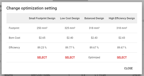
Figure 4 below is a screen shot of the new Customize screen.  You will notice that you can view your design upfront, customize parameters to the left, and see the effects of your customizations in operating and performance below.  You will also see in Figure 5 that we have removed the optimization knob. The removal of the optimization knob simplifies the process by calculating the design values upfront for comparison purposes so that you can make the best decision to meet your optimization needs.

Figure 4: Customize screen


Figure 5: Optimize your design

Once you are done customizing, you can verify your design by running an electrical simulation in the next screen.  Finally, you can move on to the export screen which displays an overview of your final design with clear buttons to prompt you to export to your most used CAD tools, print a design PDF report, or circle back to TI.com for more information such as downloading a datasheet, going to the TI Store, or exploring the product folder.

Mark your calendars for our July 5 launch date and subscribe to TI’s Power House blog community for further content on how to best navigate our new interface.


How to modify a step-down converter to the inverting buck-boost topology

$
0
0

 When looking for a DC/DC converter to create a negative voltage, in many cases you will use a step-down converter in the inverting buck-boost topology. While dedicated inverter devices such as the very-low-noise TPS63710 are easier to design with and generally a better solution, there are numerous reasons to use a step-down converter as an inverting buck-boost converter instead. First, there are relatively few dedicated voltage inverter devices in the market, compared to the ubiquitous step-down converter. You may not find a specific feature or characteristic which is required in your application. In other cases, it greatly simplifies the procurement effort to use another instance of an existing step-down converter for another socket in the design through utilizing it in the inverting buck-boost topology. Since there are generally very few inverting buck-boost circuits available for lab testing, you will need to modify the readily-available step-down converter EVM into the inverting buck-boost topology to measure the circuit for your design. This blog walks you through the steps required to take the standard TPS82130 evaluation module (EVM), which is configured as a step-down converter, and create an inverting power supply based on  3- to 11.5-VIN, –5-VOUT, 1.5-A Inverting Power Module reference design.

Using a step-down converter as an inverting buck-boost converter is a valid application use case, supported by numerous reference designs and applications notes. The TPS82130 step-down power module is used as the example, because of its high integration level and simple design. It also contains two inverting buck-boost reference designs, TIDA-01457 and TIDA-01405, with full test data and documentation. Please see the reference design guide section 2.3 for a detailed technical discussion of using step-down converters as inverting buck-boost converters.

To begin, Figure 1 shows the standard EVM as it would be connected as a step-down converter.

Figure 1: TPS82130EVM-720 connected as a step-down converter

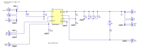
To achieve the TIDA-01457 design, its inverting schematic in Figure 3 is compared to the normal step-down EVM’s schematic in Figure 2. 

Figure 2: Step-down converter (TPS82130EVM-720) schematic

Figure 3: Inverting buck-boost (TIDA-01457) schematic

To achieve the inverting function, the output terminals are swapped such that VOUT (J4) becomes GND and the GND terminal (J6) becomes –VOUT. Everything that was GND is now labeled –VOUT. In addition, the input voltage is applied from VIN to VOUT, which is now GND.

Further comparing the two schematics, we find the remaining changes required to transform the EVM into the inverting circuit. Note that the reference designators are identical between the designs, except for the input capacitors C1 and C4 whose connections need to change from what the existing printed circuit board (PCB) provides.

Here are the required changes, which are shown in the following images:

  • Remove C1 and C4, but save them to re-install later
  • Install a 22-µF ceramic output capacitor at C6, C7, and C8
  • Change the value of R1 and R2 to set the appropriate output voltage
  • Install the input capacitors, C10 and C11, which were saved from earlier

First, the input capacitors are removed, the additional output capacitors installed, and the two feedback (FB) resistors changed.  Figure 4 shows the resulting EVM:

Figure 4: TPS82130EVM-720 partially modified to an inverting circuit

Next, the input capacitors, C10 and C11, are installed. There are no pads at the correct electrical locations on the existing EVM, so the existing pads for the VIN connection are used and a wire is added to complete the connection to GND, which is VOUT on the PCB. Figure 5 shows the result, which has completed all modifications and is now an inverting buck-boost power supply.

Figure 5: TPS82130EVM-720 completely modified to an inverting circuit

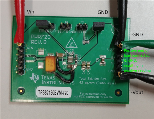
Figure 6 shows this same EVM wired in the correct way and ready to be powered on. Note that the positive terminal of the load connects to GND (J4) and the negative terminal to GND (J6). This presents the load with a positive voltage, instead of a negative one.

Figure 6: TIDA-01457 connected as an inverting buck-boost converter

These same steps and procedures are applicable to most step-down converter EVMs and allow you to quickly evaluate them as inverting buck-boost converters, without having to make a PCB of your own.

Additional Resources

Browse TI’s inverting charge pump solutions

Browse TI’s inverting buck-boost solutions


Effects of IC package on EMI performance

$
0
0

The origin of electromagnetic interference (EMI) in switched-mode power supplies can be traced back to the transient voltages (dv/dt) and currents (di/dt) generated during the switching of power metal-oxide semiconductor field-effect transistor (MOSFET) devices. With ever-growing demand for more power as well as higher switching frequencies, it is becoming increasingly challenging to address EMI in regards to device performance and meeting regulatory requirements. In this article, I’ll present an overview of the most widely used package types used for power electronics devices and their influence on EMI.

There are three common package types used in power electronics today:

  • Thin-shrink small-outline package (TSSOP).
  • Quad-flat no lead (QFN).
  • Flip-chip on lead (FCOL QFN) or TI HotRod™ package.

TSSOP

Figure 1 is a cross-section of a TSSOP and the main building blocks in this type of package design. As you can see, the integrated circuit (IC) is mounted on a lead frame (mainly using some type of epoxy) with pins protruding through the plastic housing, enabling a connection of the IC to the printed circuit board (PCB). The die connects to the lead frame using gold, aluminum or copper wires. From this cross section, you can see that the connection between the IC and a certain point on the PCB consists of the IC die (with its corresponding parasitic components); the wire-bond connection between the IC and the lead frame; and finally, the leaded physical connection between the IC package and PCB. All of these components in the connection path contribute to a generally higher resistance path, as well as increased parasitic inductance. This package is popular because of ease of assembly, relatively low cost and good thermal performance.

Figure 1: TSSOP package cross section

The question is, how do all of these TSSOP characteristics affect device EMI performance? Increased parasitic inductance will result in larger overshoot on the switch node. Package parasitic components are just a part of the overall picture, however; board layout also plays a very important role.

Figure 2 is an oscilloscope screenshot showing a switch-node waveform on a DC/DC converter in TSSOP. Increased ringing on the switch node will have a direct effect on resulting EMI performance, making it more challenging to meet required EMI regulatory compliance (for example, Comité International Spécial des Perturbations Radioélectriques [CISPR] 25 class 5 requirements). The observed ringing frequency is in the 150MHz-250MHz range.

Figure 2: Switch node waveform for the TSSOP package

QFN package

The internal construction of a QFN package is very similar to TSSOP. Figure 3 shows a simplified cross-section of this package. The active side of the IC die connects to the lead frame using wire bonds. A QFN package does not have leaded pins to connect the device to the PCB; it has connection pads on the lead frame. The main advantages of this type of package are ease of use in assembly, good thermal performance and the ability to achieve fine pitch between the package pads.

Figure 3: QFN package cross section

The absence of leaded external pins results in reduced parasitic inductance/resistance. This is visible in reduced overshoot when observing the switch node (as shown in Figure 4). The ringing frequency is noticeably different from the values observed for leaded devices, generally in the 200MHz-250MHz range. Newer device generations such as TI’s LM76002 or LM76003 are manufactured using this package, and Figure 4 shows switch-node ringing waveform.

Figure 4: Switch node waveform for the QFN package

FCOL QFN (TI brands this package as HotRod)

The FCOL QFN package was developed in an effort to further reduce switch-node ringing (as one of the contributors to EMI). In this type of package, there are no wires to connect the IC to the lead frame. Solder bumps are placed on the IC die; the die is then flipped and attached to the lead frame. Figure 5 is a package cross section.

Figure 5: FCOL QFN package cross section

The resulting performance, from the perspective of switch-node ringing, is measurably improved because there are no wires connecting the IC to the lead frame and PCB. The connection is much shorter and direct between the IC and outside world. Not surprisingly, when observing the switch-node waveform (under the same conditions as for TSSOP and QFN), there is a significant reduction (almost a complete absence) of switch-node ringing. Figure 6 shows switch-node ringing on the LM53635 device.

Figure 6: Switch node waveform for the FCOL QFN package

Based on your desired performance and application constraints, you should carefully consider package type an important selection criteria. The new device generations show significantly improved performance in terms of switch-node ringing.

Understand, however, that switch-node ringing is just one of the performance parameters that will affect EMI performance in the end application. You will need to account for several other factors such as proper input filtering, board layout and the appropriate selection of passive components for optimum performance.

Additional resources

Optimizing solar power with battery chargers

$
0
0

As solar-powered devices become more portable and interconnected, rechargeable batteries eliminate the need for AC adapter input power and take advantage of the abundant energy from the sun.

For example, devices such as e-bikes and Internet Protocol network cameras spend most of their time outside and away from power outlets, making solar charging critical for system operation. Likewise, solar-charging technology enables the collection and storage of energy in power banks during remote activities such as hiking, where the power grid is beyond reach.

Typically, a single solar cell produces about 0.7V. Consisting of several stacked cells, a panel is capable of supplying a wide range of voltages and provides input power for the charging system. Due to inconsistencies in the amount of sunlight shining on a panel, temperature variations and the high impedance of the cell stack, solar panels require operation at a maximum point to output the greatest power with the highest efficiency.

When a system must handle high source impedance and lighting variations, using a charger that steps down (bucks) or steps up (boosts) the voltages offers the best solution for solar applications. TI’s bq25703A multicell buck-boost charger transitions between buck mode and boost mode based on the battery’s charge requirements, thus successfully managing any solar voltage input. In some simpler, low-power applications, the bq25895 single-cell buck charger is an appropriate choice for solar battery charging. Both the bq25703A and bq25895 use I2C functionality to determine the maximum power point (MPP) of the system and efficiently charge the battery.

Charging for mid/high-power solar applications

Although many chargers on the market only provide buck mode, the bq25703A is able to step down or step up the input voltage to the battery. Operating at an input voltage range of 3.5V to 24V, this charger is compatible with solar panels that typically have an open circuit voltage of up to 24V. In order to efficiently use sunlight as a source of power for solar charging applications, the charger implements MPP tracking (MPPT) using input voltage regulation to achieve maximum output power.

A solar panel has an MPP on its IV curve, at which the photovoltaic system operates with maximum efficiency. Each IV curve varies based on the amount of sunlight that the panels capture; therefore, the MPP is always changing, as shown in Figure 1.

Figure 1: IV curve of a solar cell

Using the adjustable voltage dynamic power-management loop, , the charger decreases the charge current when the voltage falls below the input voltage setting. With this dynamic power-management feature, the bq25703A can therefore implement MPPT for solar applications.

When the solar panel powers the input, an MPPT algorithm adjusts the input voltage to the MPP voltage and clamps the input current to extract the maximum output power from the panel. Figure 2 illustrates a solar battery charging implementation using the bq25703A.

Figure 2: Solar charging with the bq25703A

With buck, boost and buck-boost capabilities, this charger can take a solar power input voltage that is lower or higher than what the battery requires and step up or step down to charge a one- to four-cell battery. However, if the design requires lower-power solar battery charging, the bq25895 single-cell buck mode switching charger implements an algorithm to extract an MPP.

Charging for low-power solar applications

The bq25895 provides a simple, integrated solution to solar battery charging for low-power applications. With an operating input range of 3.9V to 14V, the bq25895 is compatible with solar panels that have an open circuit voltage of up to 12V, charging a single-cell lithium-ion (Li-ion) or lithium-polymer battery. This single-cell charger implements MPPT using the charger’s integrated analog-to-digital converter (ADC).

Assuming a fixed battery voltage, the integrated ADC continuously reads the input voltage and battery-charging current while manipulating  in 100mV steps. Initially, the charge current and input current limit, , are set to their maximum limits. In most cases, the MPP of a solar panel exists within 65% to 90% of the open-circuit voltage. Therefore, in order to minimize the number of steps required to find the MPP, the algorithm limits the input voltage to that percentage range.

After the initialization of parameters, the algorithm increases  from its lower limit of 65% of the open-circuit voltage, and the ADC measures the charge current. By constantly monitoring for the maximum charging current, the algorithm can determine the MPP as it changes with varying amounts of sunlight.

Figure 3 shows the solar charging process using the bq25895. Although the device only offers bucking capabilities, the charger possesses the MPPT algorithm necessary for using solar input power and succeeds in low-power situations when boosting the input is atypical.

Figure 3: Solar charging with the bq25895

Conclusion

As the portability of technology continues to grow, devices in the market are quickly adopting rechargeable batteries to satisfy their power needs. For outdoor applications where plugs are not readily available, energy from the sun can provide the input power needed for the system. However, because sunlight intensity varies, the charger must optimize the solar input in order to efficiently output maximum power.

TI’s bq25703A and bq25895 battery chargers implement MPPT in order to select the peak output power of the solar panel. Using solar panels as a power source not only enhances the user experience by eliminating the need to search for an external power outlet, but also taps into the limitless energy provided by the sun.

Additional Resources:

Boosting efficiency for your solar inverter designs

$
0
0

With summer upon us here in the U.S., I’m already thinking about beach days and poolside BBQs. Growing up in South Florida and currently living in Texas, I’m very familiar with hot and sunny days. Similarly, I’ve gotten used to receiving higher electricity bills during this time of the year. On the bright side, sunny days also bring a lot of benefits to the table, one of them being solar energy.

Solar energy helps reduce the cost associated with generating electricity; one of the hottest topics in this industry is power conversion efficiency. Solar inverter manufacturers invest a lot of time trying to achieve even 0.1% higher efficiency. Determining how well an inverter converts the DC electricity from solar panels to the AC electricity used in homes is essential because higher efficiency correlates to increased energy generation, which translates to a faster return on investment of photovoltaic (PV) systems.

The microinverter and solar power optimizer are two rapidly growing architectures in the solar market. Figure 1 is a typical block diagram of a solar microinverter that converts power from a single PV module and is typically designed for maximum output power ranging from 250W to 400W.

Figure 1: Typical solar microinverter

To maximize PV panel performance, the front end of the microinverter is a DC/DC stage, where a digital controller performs maximum power point tracking (MPPT). The most common topology is a nonisolated DC/DC boost converter. From a single solar panel, the rail or DC link is typically 36V; for this voltage range, you can use standard silicon metal-oxide semiconductor field-effect transistors (MOSFETs) for DC/DC conversion.

Given that reduced size is a priority (so that microinverters and power optimizers will fit in the back end of a PV system); solar inverter manufactures are adopting gallium nitride (GaN) technology because of its ability to switch at higher frequencies. The higher frequency reduces the size of large magnetics in microinverter and solar power optimizer applications.

The DC/AC stage, or secondary stage, typically uses an H-bridge topology; the rail voltages are in the order of 400V for microinverters. Several isolation technologies designed to isolate the controller from the power switch and drive high-frequency switches at the same time are available today for gate drivers. These requirements are driven by safety standards for signal isolation.

TI’s UCC21220 basic isolated gate driver improves on these integration benefits by providing leading performance for propagation delay and delay matching between the high side and low side. These timing characteristics reduce losses associated with the switch since it turns on faster, while also minimizing the conduction time of the body diode, which in return improves efficiency. These parameters are also less dependent on VDD, so you can relax the design margin for voltage tolerances in the rest of the system, as the bench data in Figure 2 shows. Figure 2 also shows that the UCC21220 provides faster propagation delay than a competitor.

Figure 2: TI’s UCC21220 propagation rise/fall delay with respect to VDD vs. a competitor

The UCC21220 provides an alternative to solar applications such as microinverters and solar power optimizers where basic isolation is likely to be sufficient. Using second-generation capacitive isolation technology to reduce costs via die shrink, the UCC21220 not only helps boost efficiency by providing 28ns typical propagation delay, but also reduces printed circuit board (PCB) space and system cost.

TI’s GaN technology enables the DC/DC boost and DC/AC inverter stages to operate in excess of 100kHz. The inherent low switching losses of GaN power stages make it possible to reach efficiencies of 99% and higher.

Higher efficiencies not only mean less energy wasted, but also translate to smaller heat sinks, less need for cooling, and designs that are more compact and cost-effective. Using the right high-voltage gate drivers can help you achieve higher efficiency while reducing system cost in your space-constrained microinverter or solar power optimizer designs.

Additional resources

Why you need a programmable lighting engine when designing LED driver circuit

$
0
0
Advanced light-emitting diode (LED) animation effects like “deep breathing” and “color chasing” are becoming increasingly popular. However, a common issue designers’ face is that the microcontroller (MCU) is overloaded by captivating but complex lighting patterns. Is it possible for the LED driver to operate autonomously without MCU control? It is – with a programmable lighting engine.

Figure 1 shows a block diagram with a typical red-green-blue (RGB) LED driver, which includes a digital interface and multichannel output stage. An LED driver with an integrated programmable lighting engine includes programmable memory and a command-based pattern generator. This enables the coding of all lighting patterns as commands, which are stored in program memory inside the LED driver. When an animation effect starts, the pattern generator converts the commands and controls the output stage automatically.
 

Figure 1: LED driver block diagram
 
Without an integrated lighting engine, a system’s MCU takes full ownership of controlling and refreshing the necessary lighting patterns. This means that the MCU has to remain on, draining system power. When using a programmable lighting engine, the MCU loads the commands into the LED driver once. After that, the LED driver works as a commander to deliver programmed lighting effects autonomously, while the MCU sleeps, saving system standby power.
Let’s look at the deep breathing lighting effect as an example to better understand the benefits of a programmable lighting engine. Figure 2 shows an example.
 
Figure 2: LED animation effect example
Achieving a smooth and vivid breathing effect is easy through the commands. With the initial LEDs’ mapping configuration, you can use the ramp command to achieve programmable fade-in/fade-out effects, and set the dimming steps and dimming cycle as well. Figure 3 shows sample code.
 
Figure 3: Sample code of breathing with ramp command
Figure 4 compares MCU occupancy with and without a programmable lighting engine. With a normal solution the MCU is almost fully occupied; however, with the programmable lighting engine, the total MCU occupancy for the codes shown in Figure 3 is only 0.72mS. Obviously, the programmable lighting engine makes a real difference.


Figure 4: MCU occupancy comparison

TI has a complete portfolio of RGB LED drivers with integrated programmable lighting engines, including different channel and function options.

Additional resources

How to achieve higher system robustness in DC drives, part 2: interlock and deadtime

$
0
0

While commuting to work, waiting for a traffic light I noticed the green and red light sequence that prevents traffic flow conflicts, or crashes. The crossing traffic directions are out of sequence to ensure safe driving. Also the yellow gives a little extra time to ensure everything runs smoothly.

In a half bridge power train, such as in DC drives, it is important to make sure there are no timing conflicts between the high and low-side power devices. Like with the yellow light, there needs to be some time to make sure the power devices are not on at the same time during the switching transitions.

When selecting a gate driver for your DC drives, there are design details to consider in order to achieve higher system robustness. In part 1 of this series (How to achieve higher system robustness in DC drives part 1: negative voltage) German Aguirre discussed negative voltage spikes on the switch-node HS pin. In part 2, I’ll discuss output interlock and deadtime.

Output interlock is a feature that prevents the outputs (LO and HO) from being high at the same time, even if the inputs (LI and HI) are both high. This prevents a potentially destructive shoot-through condition in the half-bridge. To ensure that both metal-oxide semiconductor field-effect transistors (MOSFETs) cannot be on at the same time, there may be a minimum deadtime feature so that one MOSFET can switch off completely before the other switches on.

One common problem in motor control is voltage spikes and ringing on the driver input signals caused by parasitic layout inductance. Figure 1 shows the board layout trace inductances that exist in any design. These parasitic inductances should be minimized, but can never be eliminated, so a well-suited gate driver handles the transients they cause.

The red arrows in Figure 1 show an example of low-side turn on during hard switching operation: the falling VDS voltage generates a current spike upon discharge of the switch node capacitance. This high dI/dt current spike will generate a voltage because of the parasitic source inductance on the MOSFET and printed circuit board (PCB) traces. As the driver ground (COM) is typically connected close to the MOSFET source, and the controller is usually connected to a quiet ground such as the input capacitor, this voltage spike can appear on the MOSFET driver inputs.

Figure 1: Driver input voltage spikes/ringing from layout inductance

It’s important that gate drivers have features that can tolerate voltage spikes in order to ensure reliable operation and improve robustness in your designs. The UCC27710 600V driver’s interlock feature prevents the LO and HO outputs from being high at the same time, and guarantees 150-ns of deadtime between the LO and HO outputs, as shown in Figure 2. This feature will ensure that the power MOSFETs will not have an unexpected cross conduction condition caused by noise on the driver inputs. 

Figure 2: LO and HO deadtime with no LI and HI deadtime

Let’s discuss ways to reduce voltage spikes on the driver inputs. The first recommendation is the same as in part 1 of this series; reducing the parasitic inductance from the board layout. The layout of half-bridge power devices can be tight, what about the trace from the FET to the bulk input capacitor?

Figure 3 shows an example half-bridge driver and power-train layout. You can see that the MOSFETs are close together, but due to capacitor size, the bulk capacitor is often placed far from the FETs. This board layout path will result in significant source-to-capacitor parasitic inductance, which can result in large voltage spikes.

Figure 3: Board layout path resulting in parasitic inductance

Figure 4 shows the bottom layer of the same board layout. If you add high-voltage ceramic capacitors, you can place them very close to the power MOSFETs, significantly reducing the path from the low-side MOSFET source to the capacitor. Assuming that the parasitic inductance is relative to the path length, you can reduce the voltage spikes, as Figure 4 illustrates.

Figure 4: Improved board layout resulting in a reduced voltage spike

The second recommendation is to place a small resistor-capacitor (RC) filter on the driver inputs, as shown in Figure 5. The filter capacitor should be placed close to the driver and referenced to the COM pin.

Figure 5: Driver input RC filter placed close to the driver

Interlock and minimum deadtime are critical functions for gate drivers. Keep these concerns in mind to achieve higher system robustness when designing motor-drive applications.

Additional resources

The new PoE standard: It’s almost here

$
0
0

TIDA-01463 Connected LED Lighting With IEEE802.3bt Power Over Ethernet (PoE) Reference Design Board Image

This July will mark six years since the beginning of the journey for IEEE 802.3bt, the IEEE standards project that will standardize 4-pair Power over Ethernet (PoE). I began preparing for the standard when I attended my first IEEE standards meeting in July 2012. The call for interest was held eight months later, in March 2013. A study group worked until November 2013, and the task force has been building the standard ever since.

We’ve done a tremendous amount of work and I am happy to announce that we are expecting the standard to be approved in July and published in September.

The project began with the simple goal of increasing the amount of power delivered from the Power Sourcing Equipment (PSE) to the Powered Device (PD), the device that receives power from an Ethernet cable (IP phone, wireless access point, etc.). As previous PoE standards used only four of the eight conductors in an Ethernet cable to carry DC current, the task force chose to use all eight conductors for 802.3bt.

While I believe many people thought this would lead to an easy and quick standard, several issues required extensive study: how to specify parts of the previous PoE standard to work with all 4-pairs of the cable energized, backwards compatibility with the previous standard, current unbalance between all eight conductors, and four- and two-pair interoperability.

In order to convey how much work putting together a standard is, I wanted to share a few interesting facts. During development, the task force:

  • Held more than 35 in-person meetings.
  • Participated in countless phone meetings and ad hoc calls.
  • Created 24 drafts of the standard.
  • Held 22 comment review cycles.
  • Addressed more than 5,400 comments on the drafts.
  • Produced 306 pages of content in the current draft.

Throughout the process I acted as comment editor, a job involving organizing and responding to every comment received on each draft. It turned out to be much more work than I ever could have imagined. Who would have thought that over 5,400 comments would be needed to get the standard ready for publication? But in the end, it was incredibly rewarding and gave me the opportunity to learn the standard in a way that nothing else could.

Our work has resulted in a new standard that creates two new types of PSE and PDs (Type 3 and Type 4), that

  • Enables nominal power levels of up to 71.3W delivered to the PD (90W sourced from the PSE)
  • Significantly reduces the standby power required for PDs
  • creates an optional classification protocol called Autoclass that enables better power management
  • Extends physical layer classification including power demotion (and makes it mandatory)
  • Formalizes two PD configurations called single-signature and dual-signature
  • Adds Link Layer Discovery Protocol (LLDP) extensions to cover the new devices and features. Of course, we also had to solve a myriad of issues in order to make sure that four-pair PoE is the last PoE standard needed

For more details about all of these topics and more, read the white paper I coauthored for the Ethernet Alliance, “Overview of 802.3bt – Power over Ethernet standard.”

Concurrently, I have enjoyed managing the TI PoE design team and overseeing the development of five new IEEE 802.3bt-ready solutions including the TPS2373 and TPS2372. The TPS2372 is specifically targeted at applications that value our autoclass feature, such as connected lighting. Both are IEEE 802.3bt ready and come available in two different flavors, a -3 and a -4. These numbers indicate the cost-optimized integrated FET (Type 3 or Type 4).

On the PSE side of the cable, the TPS23880 is sampling and provides static random access memory (SRAM) programmability to ensure a path to compliance once the standard is officially published in September.

From the first call for interest all the way through to providing proven Ethernet Alliance-certified reference designs, TI is dedicated to making your transition to IEEE 802.3bt compliance quick and easy.


Understanding valley current limit

$
0
0

The concept of current limit seems pretty straightforward: when you increase the output current of a DC/DC converter, at a certain point it’s not possible to increase it any further. This level is the current limit, which naturally leads to the idea that the current is limited at some particular peak or maximum level.

With this in mind, the concept of valley current limit can seem quite counterintuitive. To better understand it, let’s first take a look at peak current limit.

Peak current limit

Figure 1 shows the switch-node voltage, load current and inductor current waveforms for peak current limit.

Figure 1: Peak current limit example

For a DC/DC buck converter, the output current consists of two parts: the DC load current and an AC ripple component. The DC component is the current delivered to the load, while the AC current is filtered out by the output capacitance.

The DC component is just Vout/Rload. Equation 1 expresses the AC component as the peak-to-peak inductor current:

where Vin is the input voltage, Vout is the output voltage, Lout is the output inductor and Fsw is the converter switching frequency.

During the converter on-time, the switch or inductor current rises to Iout + ILp-p/2. During the off-time, the current decreases to Iout – Ilp-p/2 and the output current is the average current. For peak current limit, the switch current is compared to the current limit value during the on-time.

In the waveforms shown in Figure 1, during Time A, the converter is regulating at a fixed-constant load current. During Time B, the load current ramps up toward the current limit set point. The converter increases the output current in each successive switching cycle by increasing the duty cycle. During Time C, the converter is operating at the current limit. When the current reaches the limit, the on-time terminates early and the off-time begins. During the off-time the current decreases back below the limit. At the start of the next switching cycle, the current starts to ramp up again. If it reaches the current limit during this cycle, the on-time once again terminates early. This type of current limit is a cycle-by-cycle peak current limit.

The switching current of the buck converter is the same for valley current limit as it is for peak current limit.

Valley current limit

Figure 2 shows the switch-node voltage, load current and inductor current waveforms for valley current limit.

Figure 2: Valley current limit example using constant on-time control

Instead of monitoring the current during the on-time, the current is monitored during the off-time. As noted, the current decreases during the off-time. At the end of the switching cycle, the switch current is compared to the valley current limit value.

In the waveforms shown in Figure 2 during Time A, the converter is regulating at a fixed-constant load current. During Time B, the load current ramps up toward the current limit set point. Since this is a constant on-time example, the converter increases the output current in each successive switching cycle by decreasing the off-time to increase the duty cycle. During Time C, the converter is operating at the current limit. When the current is above the limit, the off-time is extended until the switch current equals the valley current limit; then the next switching cycle is allowed to start.

Fundamentally, both peak current limit and valley current limit operate by increasing the off-time relative to the on-time. In the case of peak current limit, the on-time decreases and the off-time increases by the same amount, maintaining the set switching frequency. Valley current limit keeps the on-time constant while only increasing the off-time so that the switching frequency decreases during current limit operation.

Advantages and disadvantages

Now that you understand the basic operating principles, it is easy to see when each type of current limit may be appropriate. Converters using peak current mode control will typically use peak current limit. For peak current-mode control, the switch current waveform is essentially the pulse-width modulation (PWM) ramp waveform. The rising current during the on-time is compared to a level proportional to the output of the error amplifier that corresponds to the required load current. When the switch current reaches that level, the on-time terminates.

The same circuitry used to set the duty cycle can also detect the current limit by allowing an upper clamp of the control voltage. There are some disadvantages to peak current limit. The main disadvantage concerns “blanking time.” At the start of the on-time, the switch-node waveform has a very fast rise time. There may be considerable overshoot and ringing present. During this time, it is not possible to monitor the current accurately, so there is typically a minimum on-time or blanking time specified. During this time, the current is not monitored and may exceed the limit.

You can see that valley current limit keeps the on-time constant while extending the off-time to reduce current below the limit, so it would be natural to think of using this type of current limit in converters using constant on-time control modes. Constant on-time control sets the on-time to a fixed value and uses a hysteretic comparator to end the off-time when the fed-back portion off the output voltage falls below a preset level. The valley current limit will override this control signal if the current is above the limit, increasing the off-time.

Here is an advantage of valley current limit over peak current. Valley current limit is applied at the end of the off-time, before any switching transition. There is no need for any blanking time.

Another consideration is the physical location of the sensing circuit. For current limit, the actual current sometimes may not be sensed directly.  Instead, a voltage proportional to the current may be monitored. This voltage may be derived directly from the respective switch, or more typically from a smaller mirrored element. For current-mode control, this sensing element is at the high-side switch and is sensed relative to the input voltage rail. The input voltage may be variable through a large range and have significant ripple.

Valley current limit, on the other hand, senses the low-side switch current. The sensing element is referenced to the much quieter and constant circuit ground. While this is an advantage, it does have a significant limitation as well. Since valley current limit senses current at the low-side switch, it is generally limited to synchronous converters.

There is really no great mystery to valley current limit. It is just as effective as other types of current limit. The control mode used by the converter primarily determines the type of current limit.

LDO Basics: Quiescent Current 101

$
0
0

 How aggravating is it to pick up an electronic device that you’ve barely used, only to find that the battery is nearly or completely dead? If your device was just on standby or asleep, this may have happened because of a small but crucial specification: quiescent current.

What is quiescent current?

Quiescent is defined as “a state or period of inactivity or dormancy.” Thus, quiescent current, or IQ, is the current drawn by a system in standby mode with light or no load. Quiescent current is commonly confused with shutdown current, which is the current drawn when a device is turned off but the battery is still connected to the system. Nevertheless, both specifications are important in any low battery-consumption design.

Quiescent current applies to most integrated circuit (IC) designs, where amplifiers, boost and buck converters, and low dropout regulators (LDOs) play a role in the amount of quiescent current consumed. In this blog post, I’ll focus on LDOs because of their simple design and ease in calculating power dissipation. (For those unfamiliar with LDOs, the application report, “Technical Review of Low Dropout Voltage Regulator Operation and Performance” explains them in detail.) When an LDO is fully operational, Equation 1 calculates its power dissipation as:

                  (1)

For example, if you needed to drop from 4.2V to 1.8V with 200mA of output current using an LDO with 0.05mA of quiescent current, plugging those numbers into Equation 1 results in a power dissipation (PD) of:

When the application switches to standby mode or into a light load situation, quiescent current plays a much greater role in the power dissipated. Continuing from my previous example, if IOUT becomes significantly lower – 100µA, for example – PD becomes:

In this example, quiescent current contributes nearly 50% of the power dissipated.

You might be thinking, “Well, that’s not that much power being wasted.” But what about applications that spend a majority of their time in standby or shutdown mode? Smart watches, fitness trackers and even some modules on a cellphone frequently spend their time in either of those states. Fitness trackers that don’t keep their display running all the time represent a light load condition, where the IQ of the LDO used for regulation will play a significant role in battery life.

Space constraints and battery life

As the trend toward smaller and lighter consumer products continues, engineers face the challenge of decreasing size while maintaining or increasing battery life. In most instances the battery is the largest and heaviest part of the design; however, designers don’t want to physically shrink the battery because that would decrease both battery capacity and battery life. Therefore, it’s essential to keep all other onboard devices as small as possible.

Should you be concerned that you’re sacrificing performance for size? The short answer is no. TI has LDOs with peak power performance and small size because thermal resistance doesn’t need to be high for low power dissipation. The TPS7A05 is a prime example. It boasts a 0.65mm-by-0.65mm wafer chip-scale size with a 0.35mm pitch that provides 800nA of quiescent current. That is not only one of the smallest-sized LDOs, but also one of the lowest IQ devices on the market. The TPS7A05 is also made in a 1mm-by-1mm quad flat no-lead (QFN) package for designers who don’t need the 0.65mm-by-0.65mm size. This device and similar LDOs give you the best of both worlds in terms of size and performance.

Enabling your success

An enable or shutdown pin is another simple solution if you’re designing to conserve battery life. Smartwatches, fitness trackers, phones and even drones can employ this solution for a battery boost. Drones – out of all of the consumer electronics that I mentioned – spend very little time in standby mode because they’re usually only idle pre- or post-flight. You can still save battery life by shutting down LDOs attached to those modules not needed for flight. Some of these modules include the complementary metal-oxide semiconductor (CMOS) image sensor and gimbal (as shown in Figure 1), since these modules are only used when the user wants to record videos or take pictures. The shutdown current of the LDO, which is typically a few hundred nanoamps, is then the drain on the battery, which is even lower than the LDO’s quiescent current. This ultimately can give users a little bit more flight time.

LDOs are also great for the CMOS image sensor and gimbal in particular because both of these modules are sensitive to noise. Any noise reaching the image sensor or gimbal will affect the quality, resolution and stability of video or pictures taken from the drone.

You can apply this same idea to a phone’s camera, a module that also isn’t on often but still requires a clean, noiseless rail in order to maintain image quality.

Figure 1: Generic block diagram of drone modules

Conclusion

Although battery life is highly dependent on the load conditions while running, LDOs with low quiescent current are a simple solution to help boost the runtime of any battery-driven device. These small devices aren’t just limited to consumer electronics either; they play just as big of a role in industrial applications like building and factory automation. So even though designers sometimes overlook IQ and shutdown current, they could ultimately make the difference in an application running for a few more seconds, minutes, hours or even days. Now that you have learned the importance of quiescent current, so make sure to always account for it in your power dissipation calculations.

Additional resources:

FPGA power design challenges: Can I use a PMIC for that?

$
0
0

System designers gain three benefits when designing systems with a field-programmable gate array (FPGA): reprogrammability, performance scalability and fast time to market. But there are also challenges that designers must overcome. In this post, I will discuss how power-management integrated circuits (PMICs) can reduce the impact of these challenges while still providing the benefits of system-power integration.

FPGAs are popular because of their reprogrammability: designers can configure the same FPGA for many different applications, and FPGAs allow design changes late in the design cycle – even after a product has been released. Although FPGAs are easy to reprogram or reconfigure, PMICs aren’t typically associated with reprogrammability. However, PMICs with external configurability can complement reprogrammability. Externally configurable devices use external hardware such as resistors and enable pins to set the default settings of the device. When you need to change the output voltage or power-up sequence, you can easily swap external components to adjust the settings.

In Figure 1, the DC/DC buck converters set the output voltage using a resistor divider that connects from the output voltage to GND, and the center node of the two resistors connects to the feedback pin of the converter. This enables you to change output voltages easily without needing to reprogram the PMIC with the one-time programmable (OTP) or electrically erasable programmable read-only memory (EEPROM) settings. Additionally, each regulator has enable pins to enable startup. Simple sequencing requirements give you the flexibility to daisy-chain the regulators for power-up sequencing, while an external sequencing circuit or sequencer manages complex sequencing requirements.

Figure 1: External enable and resistor divider for DCDC3 on the TPS65023

TI’s Integrated Power Supply Reference Design for Xilinx Artix-7, Spartan-7 and Zynq-7000 FPGAs features a PMIC that is externally configurable such that it is easy to change the power sequencing and output voltage (Figure 2). Each regulator on the TPS65023 can be hardware-configured externally.

Figure 2:Xilinx Artix-7, Spartan-7 and Zynq-7000 FPGAs reference design block diagram

The TPS65086100 is TI’s first customer-programmable PMIC from the TPS65086xx family. You can program the device for both prototyping samples and production units. You can also program default voltages, sequencing and general-purpose input/output (GPIO) behavior into the nonvolatile OTP memory using an MSP430™ LaunchPad™ development kit with the socketed TPS650861 BoosterPack™ plug-in module. Alternatively, you can program devices directly on the board or the TPS650860 evaluation module for testing purposes. The TPS65086100 has several example configurations for quick adaptation to some of the most popular FPGAs and multiprocessor systems on chip (MPSoCs), like the Xilinx Zynq UltraScale+ family. It also has a second reserve of OTP memory in case requirements change and you need to reprogram the device.

FPGAs enable platform scalability because their cores are scalable. In general, you can turn a high-end FPGA into a low-end one for lower-powered systems. Power solutions with built-in scalability enable the system to scale with little to no redesign. PMICs with external field-effect transistors (FETs) provide output-current scalability while allowing you to stay with the same device.

For example, Figure 3 shows how the TPS6508640 can power the Xilinx Zynq UltraScale+ ZU9EG/ZU15EG family. The TPS6508640is a variant of the TPS65086x device, which has default sequencing and voltage settings programmed to the requirements of the Xilinx UltraScale+ ZU9EG. This devicehas three DC/DC controllers driving an external dual field-effect transistor (FET). Selecting the size of the FET enables you to scale the output power and maintain the same power architecture, all while powering different power levels of FPGAs.

 Figure 3: Xilinx Zynq UltraScale+ remote radio head or backhaul block diagram

Figure 4 shows an example solution that takes scalability into account for Xilinx Zynq UltraScale+ ZU2CG/ZU5EV platforms. The TPS56C215 delivers high current (up to 12A) to the core rail of the Xilinx ZU+ MPSoC. The core rail, VCCINT, requires up to 8.7A of current for the ZU5xx variant. When using a ZU2xx/ZU4xx Xilinx variant, two TPS568215 devices reduce overall cost. You can use a TPS56C215 device or an additional TPS568215 device to meet the current needs of the application because the two buck converters are pin-to-pin equivalent.

Figure 4: Xilinx Zynq UltraScale+ ZU2CG/ZU5EV MPSoC block diagram

FPGAs are often used for rapid prototyping to enable quick time to market. Figure 5 shows an example of how TI reference designs for Xilinx’s Zynq UltraScale+ ZU2CG/ZU5EV MPSoCs provide solutions specifically targeted for rapid prototyping. You can focus on routing critical high-speed data and peripheral connections to ZU+ MPSoCs and let these reference designs resolve concerns related to power supply.

The motherboard on which the Xilinx ZU+ device is mounted simply needs to use the specified Samtec connectors; you can wire your printed circuit board using Xilinx terminology. You can also combine this board with your newly designed Xilinx ZU+ motherboard prototype, plug in an AC/DC (5V, 6A out) adapter to the barrel jack of the reference design and begin testing. Sample-to-production programming for the TPS65086100 speeds time to market by allowing quick tweaks in prototyping and immediate implementation of changes in production.

Figure 5: Xilinx Zynq UltraScale+ ZU2CG/ZU5EV MPSoCs form-factor conceptual drawing

TI created several FPGA power solutions to help alleviate power-design challenges in your system, all while reaping the benefits of integrated power. PMICs solve challenges in designing FPGA-based systems related to reprogrammability, scalability and fast time to market.

The sound of GaN

$
0
0

High-fidelity (hi-fi) audio is becoming more and more popular among music fans and movie buffs, from portable speakers to high-end, in-home audio to automotive systems. And from the A to Z of classifications for audio power amplifiers, Class-D amplifiers are known for their nonlinear switching characteristics, which result in much lower power dissipation, excellent efficiency and  reduced number of system components.

Class-D audio amplifiers powered by gallium nitride (GaN) technology (also known for its superior efficiency) are enabling smaller, and more efficient  Class-D solutions than ever before.

Different than traditional Class A or Class B audio amplifiers, Class-D amplifiers use the audio signal to modulate a pulse-width modulation (PWM) signal that drives the output filtering. These devices constantly switch completely on or off, creating a highly efficient amplifier stage. For portable devices such as headphones or wireless speakers, this efficiency is critical for device battery life.

For lower-power audio amplifiers (<500W), the switching losses of the power transistor will dictate the power dissipation of the system. For a metal-oxide semiconductor field-effect transistor (MOSFET)-based amplifier to achieve hi-fi sound with a total harmonic distortion (THD) >0.1% and a reasonable power-supply rejection ratio (PSRR) of <10dB requires meticulous design work around

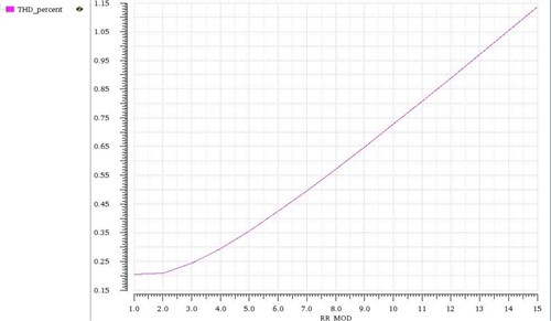
Figure 1 shows the effect on THD.

Figure 1: Deadtime vs. total harmonic distortions (THD)

GaN FETs provide superior switching characteristics, which enable even higher efficiency, better thermal sinking reduced size and weight, as well as reduced distortion for Class-D audio solutions.

GaN’s inherent characteristics provide a more ideal model of a small-signal PWM, driving the output filter. Along with this, the absence of a body diode eliminates reverse-recovery charge, which enables increased output linearity. Both characteristics allow GaN to minimize THD and ultimately create higher-quality sound.

TI’s LMG5200 is a 200V integrated GaN power stage combining a half-bridge driver and FETs into one package for an easy-to-use solution in Class-D audio. The LMG5200 offers high- to low-side matching of 2ns, which reduces distortions, and features undervoltage lockout protection (UVLO). Depending on the target of the amplifier, some designs are better suited for discrete solutions.

In order to reduce distortions that result in degraded sound quality, it is critical to minimize dead time while still preventing shoot-through current. Typical MOSFET designs will have >20ns of dead-time, resulting in distortion and power dissipation. TI’s LMG1210 200V half-bridge driver is the fastest GaN driver - capable of 50MHz switching and has resistive capability that offers adjustable dead-time control anywhere from 0-20ns. This integrated dead time control feature simplifies designs and eliminates the need for external implementation or additional software, as well as improving THD, TIMD, and EMI. The effect of dead-time on THD is simulated in the Figure 1, where the y axis is THD%, and the x axis is dead time beginning at 1 ns. The LMG1210 also offers high- to low-side matching of 1.5ns and a rise and fall time of 500ps.

Get started on your design using the LMG5200 and LMG1210 evaluation modules (EVMs) and watch the video, “How to Get Started with a GaN Power Design in Under Three Minutes.”

A review of EMI standards, part 1 – conducted emissions

$
0
0

In general, electrical products must meet some type of electromagnetic interference (EMI) performance metric, whether established in the product’s design specifications or to comply with regulatory requirements. It’s important to take into account any functional specifications that stipulate limits for EMI during the design phase of a project, particularly with respect to printed circuit board (PCB) layout and noise filtering. In part 1 of this series, I’ll review standards for conducted EMI in automotive, communications and industrial applications. Table 1 provides a list of relevant abbreviations.


IEC

International Electrotechnical Commission

CISPR 25

Comité International Spécial des Perturbations Radioélectriques, an IEC technical committee

EN 55032

A modified derivative of CISPR 32 prepared by CENELC and ratified by the EU

FCC Part 15

Federal Communications Commission; Part 15 subpart B applies to unintentional radiators

UNECE

United Nations Economic Commission for Europe

CE Mark

Conformité Européene

CENELEC

Comité Européene de Normalisation Électrotechnique

EN

European Norm

Table 1: Common acronyms.


EMI standards for automotive

From a regulatory standpoint, UNECE Regulation 10, titled “Uniform provisions concerning the approval of vehicles with regard to electromagnetic compatibility,” replaced the European Union’s (EU) Automotive Electromagnetic Compatibility (EMC) Directive 2004/104/EC in November 2014. UNECE Regulation 10 requires that manufacturers gain type approval for all vehicles, electronic subassemblies, components and separate technical units. Of course, automotive manufacturing has evolved into a global business, and the requirements and standards in this specification have broader relevance than the EU.


From an automotive electronic product designer’s perspective, the CISPR 25 product standard specifies the critical conducted emissions tests that apply at both the overall vehicle level as well as to automotive components and modules. Measurements are performed using one or two 5µH/50Ω artificial networks, depending on the grounding configuration. Conducted noise is measured over a frequency range from 150kHz to 108MHz. Because CISPR 25 refers to the “protection of onboard receivers,” the relevant frequency bands are dispersed across the AM broadcast, FM broadcast and mobile service bands, as shown in Figure 1. The limit lines in red and blue are the Class 5 peak (PK) and average (AVG) limits. PK limits are generally 20dB higher than the AVG limits.


Figure 1: CISPR 25 Class 5 conducted emission limits with peak (PK) and average (AVG) detectors


Figure 1 also plots the relevant limit lines for Class 5, the most stringent requirement from CISPR 25. Automotive manufacturers typically leverage this standard and may choose to extend or adjust the limits and frequency ranges according to their specific in-house requirements. The limits are extremely challenging, particularly the 18dBµV average (and 38dBµV peak) limit in the VHF and FM bands (68MHz to 87MHz and 87MHz to 108MHz, respectively).


EMI standards for communications equipment

Power-supply products marketed for communications products and information technology equipment (ITE) within the EU have typically used the well-known CISPR 22 (or its European Standard equivalent, EN 55022) over many years, with the CE Declaration of Conformity (DoC) for external power supplies referencing this standard to show conformance with the EU’s EMC Directive 2014/30/EU. CISPR 22/EN 55022 was recently subsumed into CISPR 32/EN 55032, however. This new standard, targeted at multimedia equipment, becomes effective as a harmonized emission standard in compliance with the EMC directive. More specifically, any product previously tested under EN 55022 that is shipped into the EU after March 2, 2017, must now meet the requirements of EN 55032.


Figure 1 shows the EN 55022/32 Class A and Class B limits for conducted emissions with quasi-peak (QP) and AVG detectors over the frequency range of 150kHz to 30MHz.


Figure 2: EN 55032 Class A and Class B conducted emission limits


Similarly, products designed for North American markets have complied with equivalent limits established by the FCC Part 15 Subpart B for unintentional radiators. Section 15.107 establishes limits for conducted emissions effectively equivalent to those in CISPR 22.


EMI standards for industrial

CISPR 11 is the international product standard for EMI disturbances from industrial, scientific and medical (ISM) equipment. Groups 1 and 2 are defined with scope for general-purpose and ISM radio-frequency applications, respectively. Each group is further subdivided in two classes: Class A equipment is for use in all establishments other than domestic and may be measured on a test site or in situ, whereas Class B covers domestic establishments and is measured only on a test site.


Meanwhile, IEC 61000-6-3 and IEC 61000-6-4 are “generic” EMC standards that apply to products targeted for residential/commercial/light-industrial and industrial environments, respectively, particularly if a product-specific standard is unavailable.


Summary

EMI is an increasingly challenging topic for fast-switching power converters. Commercial products for automotive, industrial and communications equipment are designed to minimize the amount of EMI produced during normal operation. Thus, an understanding of the EMI standards pertaining to the application is essential. The first installment of this blog series reviewed relevant standards for conducted EMI. In part 2, I’ll discuss standards for radiated EMI.


Additional resources

A review of EMI standards, part 2 – radiated emissions

$
0
0

Radiated electromagnetic interference (EMI) from switching power supplies is dynamic and situational problem that relates to circuit board layout, component placement and parasitic effects within the power supply itself, as well as the overall system in which it operates. As such, the issue is quite challenging from the system designer’s perspective, and an understanding of radiated EMI measurement requirements, frequency ranges and applicable limits is important.

Having reviewed the relevant standards for conducted EMI in part 1, part 2 of this Power House blog post series provides an overview of radiated EMI standards. Table 1 from part 1 provides a list of relevant abbreviations that are applicable here as well.

EMI standards for automotive

Assessing EMI performance in automotive applications is an issue of increasing concern for end-system designers involved in automotive design and testing. Tracking all possible interactions that might result in a radiated EMI problem is a challenge, particularly given the relatively small volume within a vehicle’s wiring harness characterized by densely packed arrangements of power and signal runs.

From a regulatory standpoint, United Nations Economic Commission for Europe (UNECE) Regulation 10 (R10.05) requires that manufacturers gain type approval for all vehicles, electronic subassemblies (ESAs), components and separate technical units (STUs). Even though this regulation emanates from Europe, it has broader relevance for other geographies, as automotive manufacturing is a global business. Figure 1 provides limits for broadband (BB) and narrowband (NB) radiated emissions over the applicable frequency range of 30MHz to 1GHz when measured using Comité International Spécial des Perturbations Radioélectriques (CISPR) 16-defined quasi-peak (QPK) and average (AVG) detectors, respectively.

Figure 1: UNECE Regulation 10 radiated EMI limits for vehicles at 10m (a); ESAs/components at 1m (b)

R10.05 refers extensively to CISPR 12 and CISPR 25, which are international standards containing limits and procedures for the measurement of radio disturbances to protect off-board and on-board receivers, respectively. CISPR 12 protects radio reception away from the vehicle and is a whole vehicle test rather than applying to subassemblies or components, whereas CISPR 25 protects radio reception in the vehicle and therefore has limit classes defined in bands for various radio services. It includes both module/component emissions measurements, as well as whole vehicle emissions tests using the antenna provided with the vehicle.

Figure 2 shows the Class 5 radiated emission limits using peak (PK) and AVG detectors for components/modules measured over a frequency range of 150kHz to 2.5GHz in a shielded enclosure. Measurements are pertinent to receivers within the vehicle operating in the broadcast and mobile service bands.

Figure 2: CISPR 25 Class 5 radiated emission limits for components/modules

Table 1 shows the antenna recommendations for various frequency ranges and the required measurement polarization. The biconical and log-periodic antenna overlap in frequency capability, whereas a broadband antenna covers the cumulative of their frequency ranges.

Frequency range

Antenna

Measurement polarization

150kHz to 30MHz

1m vertical monopole with counterpoise

Vertical only

30MHz to 300MHz

Biconical

Horizontal and vertical

200MHz to 1GHz

Log-periodic

30MHz to 1GHz

Broadband (bilog)

1GHz to 2.5GHz

Horn or log-periodic

Table 1: Measurement antenna recommendations

EMI standards for industrial equipment

CISPR 11 is the international product standard for EMI disturbances from industrial, scientific and medical (ISM) radio-frequency (RF) equipment. CISPR 11 applies to a wide variety of applications, including wireless power transfer (WPT) charging equipment, microwave cooking appliances, Wi-Fi® systems and arc welders.

Equipment in Groups 1 and 2 is delineated with scope for general-purpose and RF-specific applications, respectively. Group 1 contains all ISM equipment in which there is intentionally generated and/or conductively coupled RF energy that is necessary for the internal functioning of the equipment itself. Group 2 contains all ISM equipment in which RF energy is intentionally generated and/or used for material inspection, analysis or treatment.

Figure 3 provides CISPR 11 radiated limits for Group 1 equipment. Class A equipment is for use in all establishments other than domestic and is measured on a test site or in situ; Class B covers domestic and is measured only on a test site. I encourage you to review CISPR 11 to understand the unique specification limits and test setups for the various equipment groups and classes.

Figure 3: CISPR 11/EN 55011 Group 1 radiated emission limits using a QPK detector and measured on a test site with a 10m antenna distance 

Note that certain industrial end equipment may have dedicated system-level standards that direct EMI tests by referencing CISPR 11. For instance, International Electrotechnical Commission (IEC) 62040-2 provides EMC requirements for uninterruptible power systems (UPSs) that deliver output voltages not exceeding 1500VDC or 1000VAC. Another system-level standard, IEC 61800-3, dictates emission requirements and specific test methods for adjustable-speed motor-drive systems.

EMI standards for multimedia equipment

CISPR 22/European Norms (EN) 55022, the well-known standard for power-supply products used in information technology equipment (ITE) with a supply voltage not exceeding 600V, was recently subsumed into CISPR 32/EN 55032, creating a new product family standard for multimedia equipment (MME). Meanwhile, products designed for North American markets have complied with limits set by Section 15.109 of the Federal Communications Commission (FCC) Part 15 Subpart B for unintentional radiators.

For an antenna measurement distance of 3m, Figure 4a plots the Class A and Class B limit lines when using a QPK detector for frequencies below 1GHz. Figure 4b plots the equivalent limits above 1GHz using an AVG detector. In addition, the measuring receiver bandwidth (RBW) is set at 120kHz and 1MHz, respectively, for frequencies below and above 1GHz. Class B limits for residential or domestic applications are lower by 6dB to 10dB than Class A limits for commercial use.

Figure 4: FCC Part 15 and CISPR 22/32 radiated limits for Class A and Class B 

Summary

Radiated EMI is an increasingly challenging topic for power converters with high dv/dt and di/dt switching waveforms. Numerous governing bodies regulate the permissible levels of radiated emissions generated by an end product, and an understanding of the EMI standards pertaining to the application is essential.

Additional resources

Key considerations for designing with the new PoE standard

$
0
0

The Institute of Electrical and Electronics Engineers (IEEE) 802.3bt standard will publish in September 2018 and enable Power over Ethernet (PoE) applications up to 90W/71.3W (sent/received) such as LED connected lighting ballasts and digital signage. With the new standard fast approaching, many electronic system designers need to quickly familiarize themselves with the new features of the standard and understand key considerations for starting a new 802.3bt design.

First, power-sourcing equipment (PSE) and powered device (PD) end-equipment interoperability and compliance to the 802.3bt standard are essential. No third-party conformance suites currently exist to offer a quick IEEE802.3bt compliance check. Thus, you need to carefully consider which IC vendor is most likely to deliver solutions that are interoperable and compliant. Here are some things to look for – TI already meets all of these requirements:

  • Expertise developing both ends of the cable (powered devices [PDs] and power-sourcing equipment [PSE]).
  • Involvement in the 802.3bt standard.
  • Involvement with certification houses like Sifos Technologies and the University of New Hampshire InterOperability Library (UNH-IOL).
  • Involvement with the Ethernet Alliance (EA) logo program, whose goal is to enhance the experience of end users by minimizing interoperability issues in the market.

Key considerations for IEEE 802.3bt PSE devices

PSE with one Analog-to-digital (ADC) per port, such as the TPS23880, enables for a more robust method of meeting the new 802.3bt maintain power signature (MPS) timing requirements. The new 802.3bt MPS, which is an electrical signature presented by the PD to assure the PSE that it is still present after the operating voltage is applied, has been shorted by 10x compared to the 802.3at standard, as shown in Figure 1.

Figure 1: New IEEE 802.3bt MPS timing (green) and IEEE 802.3at MPS timing (red)

PSE devices that have one shared ADC for all ports run the risk of not being able to meet the new timing requirements. Should that occur, the PSE may remove power even if a PD is providing the desired MPS signal. For example, when an eight-channel PSE with one ADC provides power to all eight channels, the ADC must measure the current through each channel to ensure that the MPS signal is received, which could take a significantly long time to process. With solutions that have one ADC per port, there is no such concern.

Key considerations for IEEE 802.3bt PD devices

As Figure 2 shows, first consider if the autoclass feature is useful in your system. This feature allows a PD to communicate its effective maximum power consumption (including cable loss) to the PSE, enabling more efficient power budgeting. To learn more about this new feature, check out the “Understanding Autoclass in TI’s IEEE 802.3bt Powered Devices (PD)” video.

Also consider whether your design will use a single or dual PD implementation. Dual PD implementations on the market today tend to use Universal Power over Ethernet (UPOE) (a noncompliant method for delivering higher power that was deployed while the market awaited the IEEE 802.3bt standard). To learn about nonstandard high-power solutions like UPOE and how TI’s 802.3bt solutions work with nonstandard solutions, watch the “TPS23880 working with noncompliant high power PDs (UPoE, PoE++ and PoH)” and “TPS2372/3 working with noncompliant high power PSEs (UPoE, PoE++ and PoH)” videos.

Figure 2: IEEE 802.3bt PoE PD decision tree

As you can see, there are many things to consider when choosing an IEEE 802.3bt PoE PSE or PD for your design. Now that you have a good understanding as to what to consider when choosing your PoE PSE and PD devices, go ahead and start your IEEE 802.3bt design today.

Additional resources


LDO Basics: Preventing reverse current

$
0
0

In most low-dropout regulators (LDOs), current flow is like one-way street – go in the wrong direction and major problems can occur! Reverse current is current that flows from VOUT to VIN instead of from VIN to VOUT. This current usually traverses through the body diode of the LDO instead of the normal conducting channel, and has the potential to cause long-term reliability problems or even destroy the device.

There are three main components to an LDO (see Figure 1): the bandgap reference, error amplifier and pass field-effect transistor (FET). The pass FET conducts current, as any normal FET, between the source and the drain in a typical application. The doped region used to create the body of the FET, called the bulk, is tied to the source; this reduces the amount of threshold voltage change.

Figure 1: LDO functional block diagram

One drawback of tying the bulk together with the source is that a parasitic body diode forms in the FET, as shown in Figure 2. This parasitic diode is called the body diode. In this configuration, the body diode can turn on when the output exceeds the input voltage plus the VFB of the parasitic diode. Reverse current flow through this diode can cause device damage through device heating, electromigration or latch-up events.

Figure 2: Cross-sectional view of a p-channel metal-oxide semiconductor (PMOS) FET

When designing your LDO, it is important to consider reverse current and how to prevent it. In this post, I’ll cover two ways of preventing reverse current at the application level and two ways during the integrated circuit (IC) design process.

There are four common methods for preventing reverse current flow, two at the application level and two during design.

Use a Schottky diode

As shown in Figure 3, using a Schottky diode from OUT to IN will keep the body diode in the LDO from conducting when the output voltage exceeds the input voltage. You must use Schottky diodes because of their low forward voltage. Traditional diodes have a much higher forward voltage than Schottky diodes. During normal operation, the Schottky diode is reverse-biased and will not conduct any current. Another advantage of this approach is that the LDO’s dropout voltage will not increase when placing a Schottky diode between the output and the input.

Figure 3: Preventing reverse current using a Schottky diode

Use a diode before the LDO

As shown in Figure 4, this method uses a diode in front of the LDO to prevent current from flowing back into the supply. This is an effective method at preventing reverse current, but it also increases the necessary input voltage needed to keep the LDO out of dropout. The diode placed at the supply of the LDO becomes reverse-biased during a reverse current condition and does not allow any current to flow. This method is similar to the next method.


Figure 4: Reverse current prevention using a diode before the LDO

Use a second FET

LDOs designed to block reverse current flow often use a second FET to help prevent reverse current flow. The two FETs are placed with the sources back to back, as shown in Figure 5, so that the body diodes face each other. Now, when a reverse current condition is detected, one of the transistors will turn off and current cannot flow through the back-to-back diodes.

One of the biggest drawbacks to this approach is that the dropout voltage essentially doubles when using this architecture. To decrease the dropout voltage, you will have to increase the size of the metal-oxide semiconductor field-effect transistors (MOSFETs), thus increasing the overall solution size. Automotive LDOs like TI’s TPS7B7702-Q1 use this approach to prevent reverse current flow.

Figure 5: Back-to-back FETs to prevent reverse current

Connect the bulk of the MOSFET to GND

This method is the least common way of implementing reverse current but is still extremely effective, as it eliminates the body diode of the MOSFET. This method ties the bulk of the MOSFET to GND, eliminating the connection to the source that was causing the parasitic body diode. TI’s TPS7A37 uses this method to implement reverse current protection. One advantage is that tying the bulk of the MOSFET to GND does not increase the dropout of the LDO.

Figure 6: Connecting the bulk of the FET to GND

Conclusion

When reverse current protection is needed in your application look for the LDO topologies that provide the level needed. If an LDO with reverse current protection does not meet all the system requirements, consider implementing reverse current protection using a diode.

LDO basics: capacitor vs. capacitance

$
0
0

Low-dropout regulators (LDOs) provide power in all types of applications. But for an LDO to operate normally, you need an output capacitor. A common issue when designing LDOs into an application is selecting the correct output capacitor. In this post, I will explore different considerations when selecting an output capacitor and how it may affect your LDO.

What are capacitors?

A capacitor is a device used to store electric charge consisting of one or more pairs of conductors separated by an insulator. Capacitors are most commonly made of aluminum, tantalum or ceramic. Each of these materials has their own pros and cons when used in a system, as listed in Table 1. I generally recommend ceramic capacitors because of their minimal variation in capacitance, as well as their low cost.

Capacitor material

Pros

Cons

Aluminum

  • Most commonly used as low-pass filters.
  • High capacitance available.
  • Polarized.
  • Large size.
  • Large equivalent series resistance (ESR) values.
  • May overheat.
  • Limited lifetime.
  • Large leakage currents.

Tantalum

  • Small footprint.
  • Long lifetime.
  • Low leakage current.
  • Polarized.

Ceramic

  • Nonpolarized.
  • Very small size.
  • Minimal ESR values.
  • Low cost.
  • Low tolerances.
  • Thermally stable.
  • Limited selection of high capacitance.
  • DC bias derating.

Table 1: Capacitor material pros and cons

What’s capacitance?

While a capacitor is a device that stores electric charge, capacitance is the ability to store electric charge. In an ideal world, the value written on a capacitor would be exactly the same as the amount of capacitance it provides. But we don’t live in an ideal world, and so you cannot take capacitors at face value. You’ll see later that the capacitance of a capacitor may be as little as 10% of its rated value. This might be caused by derating from being biased with a DC voltage, derating from changes in temperature or manufacturer tolerances.

DC voltage derating

Given the dynamic nature of capacitors (storing and dissipating electric charge in a nonlinear fashion), some polarization may occur without the application of an external electric field; this is known as “spontaneous polarization.” Spontaneous polarization results from the material’s inert electric field, which gives the capacitor its initial capacitance. Applying an external DC voltage to the capacitor creates an electric field that reverses the initial polarization and then “locks” or polarizes the rest of the active dipoles into place. The polarization is tied to the direction of the electric field within the dielectric.

As shown in Figure 1, the locked dipoles do not react to AC voltage transients; as a result, the effective capacitance becomes lower than it was before applying the DC voltage.

Figure 1: DC voltage derating

Figure 2 shows the effects of applying voltages to a capacitor and the resulting capacitance. Notice how the larger case size loses less capacitance; this is because larger case sizes have more dielectric between the conductors, which reduces the strength of the electric field and locks on fewer dipoles.

Figure 2: Capacitance vs. DC bias vs. capacitor size

Temperature derating

Like all electronics, capacitors have a temperature rating over which their performance is specified. This temperature derating can commonly be found underneath the numerical value of the capacitor. Table 2 is a temperature coefficient rating decoder table for capacitors.

First character: low temperature

Second character: high temperature

Third character: maximum change over temperature

Character

Temperature (°C)

Character

Temperature (°C)

Character

Change (%)

Z

10

2

45

A

±1.0

Y

-30

4

65

B

±1.5

X

-55

5

85

C

±2.2

6

105

D

±3.3

7

125

E

±4.7

8

150

F

±7.5

9

200

P

±10

R

±15

S

±22

T

+22, -33

U

+22, -56

V

+22, -82

Table 2: Ceramic capacitor code table

The majority of LDO junction temperatures are usually specified from -40°C to 125°C. Based on this temperature range, X5R or X7R capacitors are best.

As shown in Figure 3, temperature alone affects capacitance much less than the DC bias derating, which may reduce capacitance values by as much as 90%.

Figure 3: Capacitance vs. temperature vs. temperature coefficient

Manufacturer tolerances

Due to the nonideal characteristics of real capacitors, the capacitance value itself may change based on the material and size of the capacitor. Companies that manufacture capacitors and other passive electronic components will have a general standard for what values of capacitance their components can tolerate. In this post, I’ll use ±20% as the manufacturing tolerance when calculating capacitance.

A real application

A common LDO application would be to take an input voltage from a 3.6V battery and drop it to power a microcontroller (1.8V). In this example, I’ll use a 10µF X7R ceramic capacitor in a 0603 package. The 0603 package refers to the dimensions of the capacitor: 0.06 inches by 0.03 inches.

Let’s find the true capacitance value of this capacitor for this application:

  • DC bias derating: By using the chart provided by the manufacturer of the DC bias characteristics for a capacitor (Figure 2), you can see that the capacitance value will be 7µF.
  • Thermal derating: If this capacitor were to be in an ambient temperature of 125°C, you would see another 15% drop in capacitance value, bringing the new total to 5.5µF.
  • Manufacturer tolerance: Taking into account the manufacturer tolerance of ±20%, the final value for the capacitance will be 3.5µF.

As you can see, a 10µF capacitor has a true value of 3.5µF when put into these conditions. The capacitance value has degraded to about 65% of the nominal value. Obviously not all of these conditions would apply, but it is important to know the range of capacitance values that a capacitor can provide for your application.

Conclusion

Although LDOs and capacitors seem simple at first, there are other factors at play that determine the effective capacitance needed for normal operation of an LDO.

Additional resources

When it comes to power process technologies, one size does not fit all

$
0
0

Power electronic system and circuit designers have more choices in power process technologies. Silicon-based devices continue to evolve, but there is also an increasing option to use wide-bandgap material technologies such as gallium nitride (GaN) and silicon carbide (SiC).

With the diversity of today’s electronic systems and applications, you need these options at your fingertips. Each technology has its strengths, and it’s imperative to understand the trade-offs in efficiency and operating characteristics in order to select the most appropriate process technology for your application.

Silicon is the most widespread and least-expensive power semiconductor material. Several innovative developments in process and device technology have helped increase the power ratings for silicon devices. Some examples of high-power silicon devices include the gate-controlled thyristor, insulated gate bipolar transistor (IGBT) and super-junction metal-oxide semiconductor field-effect transistor (MOSFET).

Silicon devices cannot process large amounts of power while simultaneously switching very fast, however, making the material less efficient in power conversion and resulting in heavier and bulkier solutions.

These challenges facilitated the development and subsequent rollout of GaN- and SiC-based devices. As shown in Figure 1, the wider bandgap and other electronic properties of GaN and SiC material enable devices that can switch higher voltages at higher switching frequencies. This is important for data centers, automobiles, smart factories, the smart grid and more. Power devices based on GaN and SiC are ultimately more efficient, resulting in smaller and lighter systems than those that are silicon-based.


Figure 1: Power technologies and position relative to power levels and frequency

GaN is an excellent choice for high-density applications below 700V, such as telecom, enterprise servers, power supplies, motor drives and photovoltaic (PV) inverters. SiC is more suitable for higher-voltage and higher-power applications. These technologies will likely drive the future of high power, with an increase in overall density and weight efficiencies. As wide-bandgap technologies mature, they will also become more cost-competitive with silicon.

The bottom line is that the landscape for power systems is changing. My new white paper outlines the overlap between the technologies and explains that no single power transistor type is the hands-down winner in every situation. The market will demand all options.

Additional resources

Dimming in switched-mode LED drivers

$
0
0

One of the key concerns in light-emitting diode (LED) driver designs is the dimming performance. Most designers use one of two methods: analog dimming or digital pulse-width modulation (PWM) dimming. There are two ways to implement digital PWM dimming: an enabling on/off approach or a shunt-field effect transistor (FET) approach. In both implementations, the LEDs will turn on or off according to the duty cycle of the digital PWM signal; yet the responses of the LED drivers are different. In this post, I will review the implementation and advantages of each dimming method.

Analog dimming uses a proportional input voltage to make a linear adjustment of the LED output current level. Many devices, like TI’s TPS92515 or LM3409 LED drivers, have a dedicated analog dimming pin with which to adjust the internal sense voltage. Alternatively, for applications with a microcontroller (MCU), the TPS92518 uses the Serial Peripheral Interface (SPI) communications interface to digitally program two internal registers to analog-dim two independent LED channels.

The drawback of analog dimming is that the current output is not linearly related to the input voltage when the required output current becomes small, due to the offset voltage of the internal operational amplifier. For example, if the LED driver’s internal operation amplifier offset voltage is ±5mV, when the sense voltage is 200mV the error of the regulated current will be 5mV/200mV = ±2.5%. When the sense voltage is 20mV, the error of the regulated current will be 5mV/20mV = 25%.

Although it is possible to use analog dimming outside the linear range, some designers prefer to stay in the linear range given the simplicity of the linear relationship. An example of analog dimming linearity is shown in Figure 1.


Figure 1: An example of analog dimming control (from the LM3409 data sheet)

Digital PWM dimming methods typically can achieve much wider linear dimming ranges than analog dimming, which is good for low brightness dimming. In the digital PWM dimming enabling on/off approach, the LED driver turns on or off according to the duty cycle of the input PWM signal, which comes from an MCU or other external source. The main delay in PWM dimming comes from turning the output drive on and off, and the subsequent ramping up and down of the inductor current. If the LED driver has a low closed-loop bandwidth, the response to the PWM signal is intrinsically slow and cannot easily achieve low brightness.

Let’s say that an LED driver runs at a 1MHz switching frequency, with its bandwidth tuned so that the output current settles within five cycles. In this case, 5µs will be the minimum turn-on time for the LED driver to provide a stable light output. If the input PWM dimming signal is 200Hz, then the period will be 5ms. In order to maintain a minimum 5µs turn-on time, the dimming ratio will be 5ms to 5µs, or 1,000-to-1. In other words, the minimum PWM dimming duty cycle will be 0.1% at a 200Hz PWM dimming frequency running at a 1MHz switching frequency. Figure 2 shows the delay of the LED current in a typical enabling on/off approach PWM dimming scenario.


Figure 2: Digital PWM dimming enabling on/off approach

To further improve the dimming performance, you could either optimize the loop bandwidth to shrink the settling time or set the LED driver to run at a higher switching frequency. The TPS92518 has two independent PWM input pins to control the brightness of the two LED channels.

Shunt-FET PWM dimming is an alternative approach that leaves the LED driver turned on. The digital PWM signal controls a shunt-FET connected to the LED load in parallel to redirect the output current flowing away from the LED through and into the shunt-FET according to the inverse of the duty cycle of the PWM signal. It’s best not to use this approach with LED drivers that require huge output capacitors because the output capacitor stored energy that might introduce high current overshoot, damaging either the shunt-FET or the LED load.

This makes LED drivers with a hysteretic control architecture such as the TPS92518 a good fit for shunt FET dimming. Hysteretic-type LED drivers are open loop, and therefore do not have the loop-bandwidth limitations of closed-loop switching-type LED drivers. The benefit of shunt-FET dimming, with a well-controlled inductor current band, is extremely fast LED turn-on or turn-off times (within nanoseconds), which enable low brightness through a low-duty-cycle PWM signal. Figure 3 shows the delay of the LED current being very small in shunt-FET PWM dimming scenario.


Figure 3: Shunt-FET PWM dimming

More and more applications require an MCU to communicate with LED drivers for brightness control. The TPS92518 has an SPI control interface to set the LED current level through an 8-bit digital byte, enabling you to adjust the LED current on the fly. The SPI control interface sets the nominal running off-time digitally instead of using a resistor-capacitor circuit on the off-time control pin. TPS92518 has another register programmed through SPI to set the maximum off-time to realize the well-controlled inductor current band during shunt-FET PWM dimming.

The TPS92518 has an internal ADC to convert the output voltages of both channels and estimated die temperature into digital code. This information is stored in the register of TPS92518 and available for read-back through the SPI interface. The architecture of the TPS92518 allows either enabling on/off PWM dimming or shunt-FET PWM dimming.

You will have to choose between analog dimming and PWM dimming to control LED brightness based on your design’s requirements. The analog dimming method does not require a digital signal input; however, deep dimming is not readily available with this method. Both implementations of the PWM dimming method can achieve a much higher dimming ratio, but require more effort to design properly.

Additional resources

How LILO LDOs increase system efficiency

$
0
0


High efficiency for power supplies has historically been attributed to switching controllers or converters, whereas designers assume that linear regulators (LDOs) have bad efficiency. But linear regulator topologies have changed to where single n-channel p-channel n-channel (NPN)/p-channel n-channel p-channel (PNP) or p-channel metal-oxide semiconductor (PMOS)/n-channel MOS (NMOS) pass transistors can help achieve very low dropout voltages.

There have been three main power-supply trends in portable systems: decreasing bus voltages, compressed voltage conversions and decreasing quiescent current (IQ). These trends have led to the development of low-input low-output (LILO) LDOs.

As bus voltages have decreased, so have the minimum input voltage requirements for LDOs. As the bus rails dropped below 1.5V, the traditional LDO topology began reaching its limits because the input voltage rail powers all of the internal circuitry. The gradually decreasing input voltage led to the increased popularity of LILO LDOs.

LILO LDOs use an NMOS pass transistor and a bias rail to achieve low dropout. The advantage of using an NMOS pass transistor is that it has a lower drain-to-source resistance (RDS(on)) than a PMOS. It also needs a positive gate-to-source voltage (VGS) to operate. As a result of this topology, the bias rail is supplied by a higher voltage and powers most of the LDO’s internal circuitry, so the LDO can operate at lower input voltages.

One of the main benefits of the NMOS transistor is the low RDS(on), which allows for a smaller dropout per unit area than the PMOS transistor, enabling  smaller dropout voltages while maintaining a small size. Figure 1 shows the typical topology of an NMOS LDO from this diagram it can be seen that a Bias pin is required for this LDO to function properly.

Figure 1: NMOS LDO Topology

As I said, the two advantages of LILO LDOs are lower input voltages and decreased dropout voltages. The latter advantage enables an increase in efficiency that is comparable to that of switch-mode power supplies. For all power supplies, you can calculate efficiency using Equation 1 as a function of the input and output power:


For a LILO LDO like the TPS7A10, you can calculate the efficiency using Equation 2, since the LDO has both a bias rail and an input voltage rail:

                   (2)

If the load current is much greater than the IQ efficiency equation can be simplified, as shown in Equation 3:

                            (3)

You can see that the quickest way to increase efficiency in LDOs is to make the input and output voltage closer together by decreasing the dropout voltage.

In portable electronics, it is very common to have LDO-powered sensors because a switching converter generates too much noise. Designers will use low-IQ LDOs, believing that they increase the battery life of the system as the load is being pulsed. This is not necessarily the most efficient solution; however, as large power dissipation during the time where the load is on can cause drastically decreased efficiency.

Figure 2 shows two common power configurations for implementing a portable system. One uses a generic low-IQ LDO and the other uses a low-IQ LILO LDO. Comparing the power dissipation between the two solutions, the generic low-IQ LDO dissipates 2.7mW, while the LILO LDO dissipates 1.8mW (see Table 1). Using the LILO LDO increased the efficiency from 55% to 82%, even though the total IQ is higher on the LILO LDO.

Figure 2: A low-IQ LDO vs. a LILO LDO

Table 1: Efficiency calculations

As you can see, there is a clear benefit to implementing LILO LDOs in portable applications if battery life and efficiency are your main concerns. Reducing the differential between the input and output voltage enables these LDOs to achieve efficiencies greater than 80%. Once you understand this, you can select the proper LDO for your application.

Additional resources

Viewing all 437 articles
Browse latest View live


<script src="https://jsc.adskeeper.com/r/s/rssing.com.1596347.js" async> </script>