Quantcast
Channel: Power management
Viewing all 437 articles
Browse latest View live

Help! My power supply unit is unstable – part 1

$
0
0

I’ve heard that there are at least seven reasons to eat, and only one of those reasons is hunger. In the same way, there are many reasons for switched-mode power supply (SMPS) instability, and only one of those reasons is a control loop with an insufficient gain or phase margin. In this six-part series, I will offer some tips about identifying the causes of these instabilities and how to fix them.

Reaching for a network analyzer to measure the loop response and study the gain and phase margins may in fact be the correct path to a solution (just as we sometimes eat because we are actually hungry), but there are quite a few situations where a gain and phase plot won’t help at all.

In all cases, the first thing you should do is look carefully at the instability, study its characteristics and use that information to deduce the likely cause.

Control-loop instability

Let’s look at control-loop instability first, because – despite what I said above – a control loop with a sufficient gain and phase margin is a necessary but not sufficient, condition for SMPS stability.

You designed your circuit to have the required gain and phase margins in order to meet your design targets and provide a stable control loop. Bode plots show the gain and phase margins in the frequency domain. The load transient response is easier to measure and gives a good qualitative indication of system stability in the time domain. The load transient response is in some ways a better indicator of system stability because it indicates the large-signal response of the system, in contrast to the small-signal response of the Bode plot. Figure 1 shows a typical Bode plot and transient response for a boost power factor correction (PFC) stage.

Figure 1: Typical loop response: Bode plot (a); transient response (b)

There are several nonlinearities in an SMPS control loop that can alter the loop gain and phase enough to change a stable loop into an unstable one:

  • The current transfer ratio (CTR) of an optocoupler in the feedback loop can change over a large range, with as much as a 3-to-1 variation as the light-emitting diode (LED) current changes from minimum to maximum, with a further 50% change as the temperature changes from room temperature to maximum temperature (20°C to 90°C, for example).
  • Inductors are sometimes deliberately designed to have a much higher inductance at light loads than at heavy loads (swinging chokes).
  • The gain of the power stage increases as it moves from discontinuous conduction mode (DCM) to continuous conduction mode (CCM).

Diagnosis and solution

Control-loop instability causes an oscillation at the loop crossover frequency (0dB gain). Ideally, the oscillation is sinusoidal, but there may be some distortion present due to nonlinearities in the system. Here is what you might see:

  • It will persist over a fairly wide range of input voltage and load current conditions. An instability present over a narrow range of operating conditions is unlikely to be caused by the control loop.
  • The duty-cycle change will be gradual over the period of the oscillation.
  • A wrong component value may have been fitted or a component may be completely absent. This will change the loop response, reducing or eliminating the gain margin designed into the loop. Carefully check the value of each of the resistors, capacitors and other components in the feedback loop.
  • Optocouplers usually have a pole in the transfer function at about 10kHz; this may be causing an unexpected extra-phase shift if you didn’t account for it at the design stage.

One approach to finding a solution is to slow the loop down, take Bode plots, study the results and recalculate the compensation networks, iterating as necessary. Don’t confuse a control-loop oscillation with an input-filter oscillation. (I’ll discuss this in a later installment of this series.) Does the oscillation persist if you short-circuit the input-filter inductors or the system become unstable due to the increase in gain as it moves from DCM to CCM?

Note that the output of a boost PFC stage will always have a sinusoidal ripple voltage at twice the line frequency. This is inherent in the topology and should not be confused with control-loop instability. The ripple is the reason that the boost PFC control-loop bandwidth is normally limited to between 7Hz and 10Hz.

Conclusion

There could be many reasons why your SMPS is unstable. In later installments of this series, I will look at some of the more common causes of instability, although my list will be far from complete.

Here are the upcoming installments I’ve planned:

  • Part 2: Subharmonic and input-filter oscillations.
  • Part 3: Source instabilities and oscillations due to remote-sensing networks.
  • Part 4: Instabilities due to the load.
  • Part 5: Instabilities due to electrical noise.
  • Part 6: Insufficient control range, leading-edge spikes, overcurrent hiccup mode, burst mode, hysteretic control.

Discover how TI is transforming your high voltage power design with end-to-end power conversion solutions that deliver high efficiency, power density and reliability:


Transform the way you charge your devices with USB Type-C and PD

$
0
0


Nowadays, we see more and more electronics with USB Type-C™ and USB Power Delivery (PD) ports on the market. They range from cellphones, laptops and power banks to drones, power tools, and smart home and portable applications. The USB PD standard allows the transmission of high power after negotiation and presents new requirements for what’s behind the port: the charger IC.

On one hand, as a device, your equipment should be able to negotiate the highest voltage (5-20V) and current provided by the source to charge the battery and provide power to the system. On the other hand, as a host, your equipment should provide the maximum voltage (5V-20V) and current from the battery in the on-the-go (OTG) direction to peripheral devices.

For devices with single- or multiple-cell lithium-ion (Li-ion) battery systems, a buck-boost battery charger is a good solution for compatibility with the requirements I’ve described. When the device is charging, a buck-boost battery charger can buck (step down) the source voltage to charge the battery if the source voltage is higher than the battery, or can boost (step up) the source voltage otherwise. When providing power to the peripherals, a buck-boost charger can buck the battery voltage if the peripheral device asks for a lower voltage, and boost if the peripheral asks for a higher voltage.

Buck-boost chargers have gained a lot of popularity as more and more applications adopt USB PD and USB Type-C ports. Take drones, for example. Drones are power-hungry devices. Depending on the power level and battery capacity, most drones can fly six to 30 minutes per charge. Due to their short flight times, it’s convenient for users to buy extra batteries and have multiple charging options, from charging from the port on the drone itself to using cradle chargers in the car or at home.

bq25703A application diagram

Because the USB Type-C port is universal and has high power delivery capability, it is a good choice here. To be compatible with power sources with different voltage and power levels, a multicell battery system, like a drone, needs to take advantage of a buck-boost charger. It’s also critical for users to be able to charge their batteries quickly and safely during flight intervals. The bq25703A and bq25700A support up to a 6.35A charging current and has extensive protection features, including input current optimization (ICO) that helps get the maximum power out of a wide variety of adapters. Figure 1 provides additional information in the bq25703A application diagram. 

Finally, a drone should operate and charge at different temperature conditions. The bq25703A family provides ±0.6% battery-charging regulation accuracy from -40°C to 85°C. This high level of charging accuracy ensures that the batteries are optimally charged across temperatures.

A buck-boost battery charger is a desirable solution for applications that use USB PD ports and require smooth transitions between operation modes, adaptability for different adapters and extensive safety features.

Additional resources

How to approach a power-supply design – part 3

$
0
0

In the second installment of this blog series, I discussed how to choose the best-fitting topology from the parameters of your power-supply specification. In this third installment, I’ll describe different in-depth aspects for buck, boost and buck-boost topologies.

Buck converters

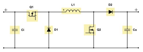
Figure 1 shows the schematic of a nonsynchronous buck converter. A buck converter steps down its input voltage to a lower output voltage. The energy transfers to the output when switch Q1 is conducting.

Figure 1: Schematic of a nonsynchronous buck converter

Equation 1 calculates the duty cycle as:

Equation 2 calculates the maximum metal-oxide semiconductor field-effect transistor (MOSFET) stress as:

Equation 3 gives the maximum diode stress as:

where  is the input voltage,  is the output voltage and  is the diode forward voltage.

The bigger the difference between the input voltage and output voltage, the greater the buck converter’s efficiency compared to a linear regulator or low-dropout regulator (LDO).

While a buck converter has a pulsed current at the input, the output current is continuous due to the inductor-capacitor (LC) filter located at the converter’s output. As a result, the voltage ripple reflected to the input will be larger compared to the ripple at the output.

For buck converters with a small duty cycle and output currents greater than 3A, I recommend using a synchronous rectifier. If your power supply requires output currents greater than 30A, I recommend a multiphase or interleaved power stage, as this minimizes the stress for components, spreads the generated heat among multiple power stages and reduces the reflected ripple at the converter’s input.

Duty-cycle limitations can occur when using an N-FET, because the bootstrap capacitor needs to be recharged every switching cycle. In this case, the maximum duty cycle is in the range of 95-99%.

Buck converters have in general good dynamic behavior because they represent a forward topology. The achievable bandwidth depends on the quality of the error amplifier and the chosen switching frequency.

Figures 2 through 7 show voltage and current waveforms in continuous conduction mode (CCM) for the FET, diode and inductor in a nonsynchronous buck converter.

Boost converters

A boost converter steps up its input voltage to a larger output voltage. The energy transfers to the output when switch Q1 is not conducting. Figure 8 is a schematic of a nonsynchronous boost converter.

Figure 8: Schematic of a nonsynchronous boost converter

Equation 4 calculates the duty cycle as:

Equation 5 calculates the maximum MOSFET stress as:

Equation 6 gives the maximum diode stress as:

where  is the input voltage,  is the output voltage and  is the diode forward voltage.

With a boost converter, you can see a pulsed output current, as the LC filter is located at the input. Thus, the input current is continuous and the output voltage ripple is larger than the input voltage ripple.

When designing a boost converter, it is important to know that there is a permanent connection from the input to the output, even when the converter is not switching. You have to take precautions in case of a possible short event at the output.

For output currents greater than 4A, you should replace the diode with a synchronous rectifier. In case your power-supply needs to provide output currents greater than 10A, I highly recommend a multiphase or interleaved power-stage approach.

When operating in CCM, the dynamic behavior of a boost converter is limited due to the right half-plane zero (RHPZ) of its transfer function. Because the RHPZ cannot be compensated, the achievable bandwidth will usually be less than one-fifth to one-tenth the RHPZ frequency. See Equation 7:

where  is the output voltage,  is the duty cycle,  is the output current and  is the inductance of the boost converter.

Figures 9 through 14 show the voltage and current waveforms in CCM for the FET, diode and inductor in a nonsynchronous boost converter.

Buck-boost converters

A buck-boost converter is a combination of a buck and a boost power stage, which share the same inductor. See Figure 15.

Figure 15: Schematic of a two-switch buck-boost converter

The buck-boost topology is useful because the input voltage can be smaller, greater or equal to the output voltage, while the output power needed is bigger than 50W.

For an output power smaller than 50W, a single-ended primary inductance converter (SEPIC) is a more cost-effective choice because it uses less components.

A buck-boost converter operates in buck mode when the input voltage is greater than the output voltage, and in boost mode for input voltages smaller than the output voltage. When the converter is operating in the transfer region, which is when the input voltage is in the range of the output voltage, there are two concepts for handling these conditions: either both the buck and boost stage are active at the same time, or the switching cycles alternate between the buck and boost stages, each usually running at half the regular switching frequency. The second concept can cause subharmonic noise at the output and the output-voltage precision can be a little bit less accurate compared to regular buck or boost operation, but the converter will be much more efficient compared to the first concept.

The buck-boost topology has pulsed currents at the input and the output, as there is no LC filter pointing in either direction.

You can use the buck and boost power-stage calculations, respectively, for a buck-boost converter.

Buck-boost converters with two switches are suitable for a power range between 50W and 100W (such as the LM5118), with synchronous rectification up to 400W possible (as with the LM5175). I advise using synchronous rectifiers with the same current limits as for the uncombined buck and boost power stages.

You need to design the compensation network of a buck-boost converter for the boost stage, because the RHPZ will be the limiting factor of the regulator’s bandwidth.

In my next post, I will discuss the features and drawbacks of the SEPIC and Zeta converter.

Additional resources

The story behind "Fundamentals of Power Supply Design"

$
0
0

I joined Texas Instruments in July 2003, working in marketing for power management. During my first week on the job, my boss introduced me to Bob Mammano like this: “Tim, I’d like to introduce you to Bob Mammano, the inventor of the first integrated circuit [IC] designed for switch-mode power-supply control.”

Bob was managing TI’s worldwide Power Supply Design Seminars at the time and was in our office to meet with our technical experts. It was quite a memorable moment to meet an icon of the power-supply industry.

Fast forward to January 2016 – my boss explained a new project that he wanted me to manage like this: “Tim, I’d like you to work with Bob Mammano and create a power-supply textbook that draws upon the technical content from our three decades of Power Supply Design Seminars.”

My background is product marketing for power-management ICs, but I have very little knowledge of publishing books.

We introduced “Fundamentals of Power Supply Design” in March 2017. Written for new engineering graduates as well as seasoned power supply designers, this textbook features theory, equations and actual circuit-design techniques. It is a useful reference of power-supply technology for designers of all levels of experience.

Often considered “the father of the PWM controller industry,” Bob is a pioneer in the power electronics field with more than 50 years of experience in analog power control. He became heavily involved in the TI Power Supply Design Seminar, both in the preparation of topics and in their presentations worldwide. It was the materials from these seminars that served as the framework for the book.

To provide some perspective on the scope of the work that went into producing the book, “Fundamentals of Power Supply Design” has 331 pages of text, 81,595 words, references 58 seminar topics, and hundreds of figures and equations. Some of TI’s best power systems engineers reviewed Bob’s writing – experts themselves in selected topics whose contributions ensured that the material was up to the high standards we were aiming for.

For example, Robert Kollman was reactivated out of retirement from a career as head of TI’s Power Design Services group. I’ve known Robert for as many years as I have been with TI and his contribution to the power-supply industry is vast and well known. Robert was the chief technical editor of the book and also authored Chapter 13, “Power Supply Construction.”

The book begins with the basics of switch-mode power-supply design such as voltage regulation and power-supply components and then expands into more advanced topics such as topology selection, control algorithms and power-supply construction. Topics are well supported by theory and equations, with actual measurements used throughout to illustrate practical example circuits.

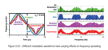
Figure 1, featured in Chapter 9, is a good example of how four-color printing helps in displaying measurements taken for frequency spreading.

We introduced “Fundamentals of Power Supply Design” in March 2017. Written for new engineering graduates as well as seasoned power supply designers, this textbook features theory, equations and actual circuit-design techniques. It is a useful reference of power-supply technology for designers of all levels of experience. 

Figure 1: Different modulation waveforms have varying effects on frequency spreading

Chapter 7 tackles one of the more difficult topics power-supply designers must work with: magnetic component design (Figure 2).

Figure 2: Table of contents: Magnetic component design

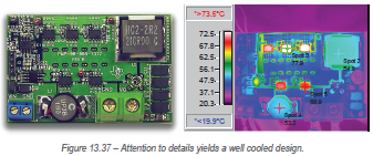
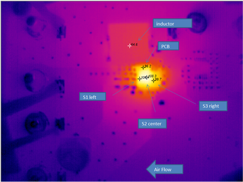
Chapter 13 uses actual circuit examples to illustrate power-supply construction. Figure 3 shows thermal imaging of an actual board.

Figure 3: A solution for cooling a power supply through the PCB surface

Interesting historical and behind the scenes facts give the subject matter overall context. For example, Bob chronicles the time they created Under Voltage Lock Out (UVLO).  When designing the first PWM control chip, Bob thought they had designed in all the control functions required, and initial testing in several power supply applications seemed to confirm success. However, shortly after releasing the first prototype, they received word that a customer’s system had a very slow turn-on time and both output drivers came on when the chip voltage was slightly lower than that required to make the timing circuitry functional. This led Bob and the team to invent a new function- Under Voltage Lock Out (UVLO) – which of course is now an obvious inclusion in every controller.

From power supply basics, such as voltage regulation and power component selection to advanced topics such as magnetics design, minimizing EMI and topology selection, “Fundamentals of Power Supply Design” is a must-have resource for both new engineers and seasoned power supply designers. Get a copy of “Fundamentals of Power Supply Design” and let me know what you think.

LDO basics: noise – part 2

$
0
0

In my last blog, LDO basics: noise – part 1, I discussed how to lower output noise and control the slew rate by using a capacitor in parallel with the reference voltage (CNR/SS). In this post, I’d like to discuss another method to lower output noise: using a feed-forward capacitor (CFF).

What is a feed-forward capacitor?

A feed-forward capacitor is an optional capacitor placed in parallel with the top resistor of the resistor divider, as shown in Figure 1.

Figure 1: An NMOS low-dropout regulator (LDO) using a feed-forward capacitor

Much like the noise-reduction capacitor (CNR/SS), adding a feed-forward capacitor has multiple effects. Chief among these are improved noise, stability, load response and power-supply rejection ratio (PSRR). (The application report, “Pros and Cons of Using a Feedforward Capacitor with a Low-Dropout Regulator,” covers these benefits extensively.) It’s also worth noting that a feed-forward capacitor is only viable when using an adjustable LDO because the resistor network is external.

Improved noise

As part of regulation, the error amplifier of the LDO uses the resistor network (R1 and R2) to increase the gain of the reference voltage, much like a noninverting amplifier, to drive the gate of the FET accordingly. The DC voltage of the reference will be gained up by a factor of . However, given the bandwidth of the error amplifier, you can also expect amplification in some portion of the AC elements of the reference voltage as well.

By adding a capacitor across the top resistor, you are introducing a shunt for a particular range of frequencies. In other words, you are keeping the AC elements in that frequency range within unity gain, where R1 simulates a short. (Keep in mind that the impedance properties of the capacitor you’re using determine this frequency range.)

You can see the reduction in noise of the TPS7A91 by using different CFF values in Figure 2.

Figure 2: TPS7A91 noise vs. frequency and CFF values

By adding a 100nF capacitor across the top resistor, you can reduce the noise from 9μVRMS to 4.9μVRMS.

Improved stability and transient response

Adding a CFF also introduces a zero (ZFF) and pole (PFF) into the LDO feedback loop, calculated with Equations 1 and 2:

ZFF = 1 / (2 x π x R1 x CFF)                               (1)

PFF = 1 / (2 x π x R1 // R2 x CFF)                    (2)

Placing the zero before the frequency where unity gain occurs improves the phase margin, as shown in Figure 3.

Figure 3: Gain/phase plot for a typical LDO using only feed-forward compensation

You can see that without ZFF, unity gain would occur earlier around 200kHz. By adding the zero, the unity-gain frequency pushes a little to the right (~300kHz) but the phase margin also improves. Since PFF is to the right of the unity-gain frequency, its effect on the phase margin will be minimal.

The added phase margin will be evident in the improved load transient response of the LDO. By adding phase margin, the LDO output will ring less and settle quicker.

Improved PSRR

Depending on the placement of the zero and pole, you can also strategically lessen the gain roll-off. Figure 3 shows the effect of the zero on gain roll-off starting at 100kHz. By increasing the gain in the frequency band, you will also improve the loop response for that band. This will lead to improvements in PSRR for that particular frequency range. See Figure 4.

Figure 4: TPS7A8300 PSRR vs. frequency and CFF values

As shown, increasing the CFF capacitance pushes the zero leftward. This will lead to better loop response and corresponding PSRR at a lower frequency range.

Of course, you must choose the value of CFF and the corresponding placement of ZFF and PFF so that you don’t introduce instability. You can prevent instability by following the CFF limits prescribed in the data sheet. A large CFF can also introduce other problems outlined in the aforementioned application report.

Table 1 lists some rules of thumb regarding how CNR and CFF affect noise.

Parameter

Noise

Low frequency

(<1kHz)

Mid frequency

(1kHz-100kHz)

High frequency

(>100kHz)

Noise-reduction capacitor (CNR)

+++

+

No effect

Feed-forward capacitor (CFF)

+

+++

+

Table 1: Benefits of CNR and CFF versus frequency

Conclusion

As shown, adding a feed-forward capacitor can lead to improvements in noise, stability, load response and PSRR. Of course, you must carefully select the capacitor to maintain stability. When coupled with a noise-reduction capacitor, ac performance can be greatly improved. These are a just few tools to keep in mind for optimizing your power supply.


Additional resources:


Display Power: Why TFT LCD needs Temperature Compensation

$
0
0

If you ever had the pleasure to design the bias supply for a Thin Film Transistor Liquid Crystal Display (TFTLCD) module and you used the appropriate part from TI then you may have run into the temperature compensation function. This blog will handle the background on why a Liquid Crystal Display (LCD) needs temperature compensation and how it is implemented in TI’s LCD Bias IC’s.

Before I evaluate the temperature effect let’s touch quickly on how the LCD actually shows a picture.

A LCD is built up like a sandwich. The actual liquid crystal is covered with two plates of glass, the upper side coated with the color filter and polarizer, the lower plate deposited with TFTs to address the pixels and a polarizer as well. The actual light is coming from the backlight at the bottom. Since the 70's we know that the liquid crystal twists if an electric field is applied. Dependent on the voltage level the crystal aligns such that it either blocks or passes the backlight.

Figure 1: LCD profile 

Each pixel consists of three sub-pixels with different color filter (Red, Green and Blue). Each of the sub-pixels is controlled by a TFT, see the structure and equivalent circuit in Figure 2.

Figure 2: Unit Pixel Structure + Equivalent Circuit 

The actual picture information (data line) decides the level of voltage across the crystal (equivalent to the storage capacitor Cs and the liquid-crystal capacitor Clc).

The time frame to activate the pixel is set by the voltage at the gate of the TFT (gate line).

Now, a positive voltage (also commonly called VGH or VON) is applied to the gate and the TFT (here N-channel) turns on. Clc and Cs charge up to the voltage applied to the data line. The maximum voltage on the data line is called AVDD or VS. This is transferred to the pixel electrode and becomes visible. Vice versa, a negative voltage (also called VGL or VOFF) turns off the transistor, the intrinsic capacitors of the LC discharge and the data voltage will not be transferred.

On a FHD / 60 Hz display for example each cycle (turn-on, turn-off) needs to happen within approx. 10 µs. *FHD = 60 Hz / (1920 x 1080 pixel x 3 (RGB))  = 9.6 µs

Temperature has two big impacts on the performance of the LCD.

The first is that the actual LC fluid changes its viscosity over temperature. At cold temperatures, the viscosity of the LC fluid decreases and this increases the response time of the crystal to the applied voltages. This effect comes with the LCD technology and can only be tailored accordingly by the panel supplier.

The second effect is that the operating conditions of the TFTs are changing. Studies have shown that the threshold voltage of an amorphous silicon (a-Si) TFT increases as the temperature decreases. Figure 4 shows how this can affect the on-time transition (VGH). In a warm environment (25°C to 80°) the thresholds are quite low, the transistor switches fast enough to make sure that the picture information (Data Line) is put through to the pixel and transfers the correct light intensity.

However, cold temperatures cause the switch to turn on slower. This steals time (tΔth) to put through the picture information, see figure below. Less light comes through the filter glass and the contrast gets lower. Visible results are flickering and/or image sticking of the display. 

Figure 3: Temperature Behavior TFT

In order to maintain the correct throughput of the picture information at a lower temperature, the turn-on voltage VGH needs to be increased. This is where the temperature compensation kicks in. From the experience with panel suppliers, it is an empirical approach to set the hot and cold voltage requirements.

How is the temperature compensation implemented?

If you need to build up your own compensation network, the simplest solution to adjust a temperature dependent voltage is the circuit as below:

Figure 4: Simple Compensation Network


The most common way to measure the ambient temperature is to use a negative temperature coefficient thermistor and place it on the LCD control PCB where it represents the ambient temperature the best. As described the LCD module should specify the normal operating turn-on voltage VGH and the temperature coefficient requirements. With this, you can apply the thermistor in parallel to the upper resistor of the feedback network of the voltage regulator. This solution has the disadvantage that the voltage cannot be monitored and cannot be covered by a maximum and a minimum value. Many of today’s LCD bias solutions are programmable with an I2C compatible interface and feature the temperature compensation with an NTC thermistor network. 

Let’s take the TPS65642 for example. Figure 5 shows the block diagram of how the gate-charge voltage rail VGH can be compensated in this part. 

Figure 5: Temperature Compensation Network TPS65642


The external resistive voltage divider RT1, RT2 and RNTC sinked by a fixed current source ISET set the initial voltage and the adjustment range from TCOLD  to THOT. Use this calculation sheet to get the maths.

Once the temperature corners are set on hardware the device needs to be programmed with the voltage corners VGH(HOT) and VGH(COLD). The value for VGH(COLD) , usually the upper value is set in DAC1 (25 V to 40 V scaled down to 0.893 V to 1.429 V) and the value for VGH(HOT) , usually the lower value is set in DAC2 (16 V to 30 V scaled down to 0.571 V to 1.107 V).

The resistance of the NTC network increases with decreasing temperature. This means that the voltage on TCOMP increases with decreasing temperature. If the voltage exceeds the lower corner, Q1 turns on and sets the signal for the PWM controller to increase VGH. The resistive dividers R2/R1 set the transition slope and R3/R4 is the feedback divider for VGH.

It is also possible to set a positive temperature slope. For this, you either use a PTC thermistor instead or place the NTC thermistor parallel to the upper resistor RT1.

If you have experienced your panel having different requirements regarding temperature behavior just leave your comment below, we are interested to know.

A smart solution to sequence and monitor multiple power rails in a system

$
0
0

Electronic systems that include a central processing unit (CPU), digital signal processor (DSP), microcontroller (MCU), field-programmable gate array (FPGA) or application-specific integrated circuit (ASIC) can have multiple voltage rails and require certain power on/off sequences in order to function correctly. TI’s UCD9090A power-supply sequencer and monitor with Advanced Configuration and Power Interface (ACPI) support can control up to 10 voltage rails, ensures correct power sequences during both normal and fault conditions, and includes a dedicated fault pin to easily cascade multiple devices.

The UCD9090A is an upgrade to the former UCD9090 (listed as not recommended for new designs [NRND]). In this post, I will explain the differences between the two devices, including their operation and features, and how to migrate from the UCD9090 to the UCD9090A.  Table 1 lists the features included with the new UCD9090A.

Features

UCD9090A

UCD9090

Fault pin (enables single to cascading multiple UCD9090A devices)

Yes

No

General Purpose Input (GPI) fault response

Yes

No

GPI debugging

Yes

No

Rail state

Yes

No

Fault/peak logging disable

Yes

No

Logic General Purpose Output (LGPO) sequence on/off dependency

Yes

No

Non-volatile (NV) fault log

26

30

Rail sequence on/off timeout

140m

32s

Cold boot mode

Yes

No

Table 1:  Comparison of features of the UCD9090 and UCD9090A

What is a fault pin?

The fault pin is a new feature that enables you to cascade multiple TI UCD9090A devices with fault-pin capability. The fault pin is a bidirectional signal connected to a fault bus. The fault bus is pulled up to 3.3V by a 10K resistor. When no fault exists on a particular UCD9090A device, the fault pin is a digital input pin that listens to the fault bus. When one or multiple UCD9090A devices detect a rail fault, the corresponding fault pin turns to the active driven low state, pulling down the fault bus and informing all other UCD9090A devices of the corresponding fault. This way, coordinated action can occur across multiple devices. After the fault is cleared, the state of the fault pin turns back to an input pin. A diagram showing use of a fault pin is show in Figure 1.

Figure 1: Example using a typical fault pin

What is the GPI fault response?

This feature solves the issue of limited Analog Monitor (AMON) pins. For example, in the UCD9090, when all 10 rails are assigned to a voltage monitor; the system does not have the capability to monitor one more external event (e.g., OVER_TEMP) or one more rail. With the GPI fault response feature in place, the external event or POWER_GOOD of the point of load (POL) could connect to the assigned GPI. When the signal changes to de-asserted, the UCD9090A can help shut down the rails and retry and re-sequence the system based on how the GPI fault-response is configured.

What is GPI debugging?

To avoid triggering the PMBus alert, response fault or continue system watchdog during board-level debug or programming, a GPI pin can be assigned to perform a GPI debugging function on the UCD9090A. When asserting the assigned GPI, the device is under the GPI debug mode. The device will not activate the PMBus alert pin for any faults/warnings nor respond to any fault response. It will not log any faults, will suspend system watchdog and ignore the sequencing dependencies for rails.

What is the LGPO sequencing on/off dependency?

The UCD9090 only supports sequencing dependencies over rail and GPI. If users want to have sequencing dependencies on the LGPO, they have to physically wire the LGPO signal back to one of the GPIs. This approach requires two extra pins which could be an issue for applications that have limited pins available. The LGPO sequencing dependency feature was introduced with the UCD9090A to save the two extra pins for other functions.

What is the rail state?

Each device has up to nine states: INIT, IDLE, SEQ_ON, TON_DELAY, RAMP_UP, REGULATED, SEQ_OFF, TOFF_DELAY and RAMP_DOWN. The state of the rail can help you easily determine the status of the system so that you can more easily bring up or debug the power system. Figure 2 shows how the rail states are changed. 

Figure 2: Rail state machine diagram

What is cold boot mode?

Cold boot is a feature specifically designed for cold-temperature applications like telecom. It has the intelligence to heat up a system by turning on the cold boot rails for certain amounts of time when it is experiencing extremely cold temperatures. The UCD9090A device communicates with the system through a particular GPI called the thermal-state GPI, which is a digital output from a thermal sensing device. The cold boot feature is fully configurable, enabling you to select enable/disable, the number of cold boot rails and the timeout period. Figure 3 is a pseudo processing call of how cold-boot is handled by the device. 

Figure 3: Cold-boot processing call

Will TI continue to offer the UCD9090?

Having these new features makes the UCD9090A a better candidate over the UCD9090 for various applications, but note that TI will continue supporting and building the UCD9090 until it reaches ten consecutive years of no sales.

Migrating from the UCD9090 to UCD9090A

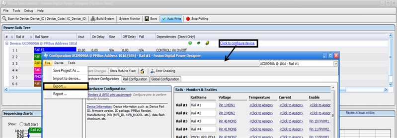
The UCD9090 and UCD9090A are pin-to-pin compatible devices. The UCD9090A supports all features of the UCD9090. Moving to the UCD9090A does not require any schematic changes. Moreover, you can seamlessly import the project file (.xml) file generated from the UCD9090 into the UCD9090A with TI’s Fusion Digital Power Designer TM GUI to help reduce the migration effort.

Because of the new features, the script file (.csv) and data flash image file (.hex, .x0) are not compatible between the UCD9090 and UCD9090A. You cannot import files generated from the UCD9090 into the UCD9090A because the device will not function as expected. To use script file or data flash image file on the UCD9090A, follow these steps:

  1. Install www.ti.com/tool/fusion_digital_power_designer and open the latest Fusion Digital Power Designer GUI.
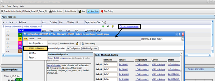
  2. Import the old UCD9090 project (.xml) into the UCD9090A. See Figure 4.

Figure 4: Import the UCD9090 project file

3. Once you have successfully imported the project, use the export function from the Fusion Digital Power Designer GUI to regenerate the .csv/.hex file. See Figure 5.

Figure 5: Fusion Digital Power Designer GUI Export Settings

4. Use the .csv/.hex file generated from step No. 3 for any programming utilities.

Hopefully this blog post provides you with a good comparison between the two devices and will help you migrate from the UCD9090 to the UCD9090A. If you have any additional questions, please post a response below or submit through TI’s E2E™ Community Sequencers forum.

Powering the smart home with a simple charger

$
0
0

Advancements in wireless connectivity and low-power embedded processing technology have enabled new applications for smart homes and buildings. Of course, most smart home systems have a control panel or base unit in a fixed location that plugs into the AC power system. But there may also be a number of distributed (and movable) wireless sensors or cameras that are part of the overall system. These peripheral devices are not always near a permanent power source.  Figure 1 shows a typical system with multiple remote peripheral devices and a central gateway (controller).

Figure 1: Example of a smart home

Many of these wireless sensors or cameras will need batteries and frequent use requires regular battery replacement, adding to maintenance costs over time. As a result, rechargeable batteries are becoming more popular for these modular accessories. In some cases, the control panel unit has a battery as well to provide backup power or an alarm in case of AC power failure.

If you are developing a smart home system, you probably want to focus your efforts on system functionality and not the basic task of power supply and recharging. Since lithium-ion batteries have become so common in recent years, there are numerous choices for dedicated battery-charging IC solutions.

For small batteries and low charge currents, you can use a cost-effective (and relatively easy to implement) linear charger. But higher-performance peripheral devices such as high-resolution cameras may need a larger battery to ensure long run times. That means you’ll need more charge current, which will require a switch-mode charger. Otherwise, the amount of heat generated due to power loss in a linear charger will be excessive.

Unfortunately, many higher-current switch-mode chargers require software control from a host processor – which is an additional investment of engineering time on your part. The benefit of these programmable chargers is that you have the flexibility to adapt the circuit to different battery types and charging currents. Other switch-mode chargers may require external power FETs or current-sensing components to enable variable charge currents.

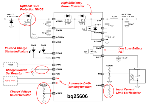
How can you have an adjustable, flexible solution for different battery types without having to invest in software development or lay out a complex PCB? This is where the bq25606 charger comes in. The circuit shown in Figure 2 provides all of the functionality needed for a typical single-cell charging and system power solution. The bq25606 enables you to optimize your charge current as well as the battery terminal voltage with just a couple of resistor values. It also has built-in overvoltage protection to guard against power line or connection transients, and can automatically detect the power available from most standard USB power sources.

You can adjust the input current limit and charging current and set the battery voltage (4.2V, 4.35V or 4.4V as needed for a given battery type) with just a few simple external component selections. If you need an easy-to-use, general-purpose battery-charging solution, “smart” doesn’t have to be complicated.

Figure 2: bq25606 implementation schematic

In a dynamic and evolving market, the success of your end product may depend getting to market faster than the competition.  Assuming that you are using a standard type of Li-Ion power source, you can use a simple, ready-to-go standalone charging solution to save time compared to a developing a customized or programmable solution.  With the bq25606, you can optimize the charge current and voltage settings with a few simple component selections and be up and running in minutes!

Additional resources:


Are you on-board? Demystifying EV charging systems

$
0
0

Electric vehicles (EVs) are an unavoidable topic when discussing modern transportation. Coming from Germany, a country that takes pride in their automotive history, the EV market is growing fast. I would consider buying an electric car in the near future, as would many others.

According to several forecasts, the market for EVs will increase dramatically, from 500,000 in 2015 up to 41 million by 2040. The global governmental growth target is even higher: 100 million electric cars and 400 million electric two- and three-wheelers on the streets by 2030.

Two of the key considerations when buying an EV are charging time and maximum range. Long charging times and the lack of an existing DC charging infrastructure are drawbacks for many potential consumers. With the rapid growth of this market also comes the rapid development of fairly substantial integrated onboard chargers (one to six hours) and fast charging piles (10-30 minutes).

Let’s go deeper into some definitions and characteristics of the two different charging systems: onboard chargers and fast charging piles.

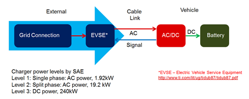
An EV or hybrid electrical vehicle (HEV) uses onboard chargers to convert line current (50/60Hz AC) to DC and to provide an isolated DC output to charge the traction battery, as shown in Figure 1.

Figure 1: High level system block diagram- on-board charger

An EV usually consists of two lead-acid batteries operating at 12V and 48V, and one lithium-ion (Li-ion) battery operating at a higher voltage of around 400V. The two lead batteries support the starter and internal systems, while the 400V battery serves as the energy source for driving.

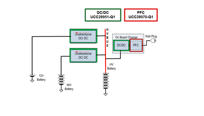
Onboard charger modules are normally two-stage converters: the input stage uses a power factor correction (PFC) module in the AC/DC power supply with a 400VDC output, which is then fed into the next stage, an isolated DC/DC converter, as shown in Figure 2. This provides galvanic isolation and a constant voltage and current output, which is necessary for efficient battery charging.

Figure 2: PFC and DC/DC controller for on-board charger

The unidirectional high- to low-voltage converters then charge the 12V and 48V lead-acid batteries from the 400V Li-ion battery’s high-voltage bus.

A fast charging pile has the same properties as an onboard charger module except that the PFC stage is off-board, driving a DC link up to 600V. This ability to reach a higher voltage is the reason why this system achieves faster charging times than the onboard system.

But what is PFC and why is it necessary? You can find PFC in isolated AC/DC power supplies, where it efficiently transmits energy from the power grid to the end system.The PFC draws an in-phase sinusoidal current from a sinusoidal source. This reduces the peak and harmonic currents and maximizes the power drawable from a given AC source – a household socket, for example. Usually any electric equipment that uses 75W or more from the grid is required to use PFC.

TI’s AC/DC solution for both charging systems is the UCC28070-Q1 interleaved continuous-conduction-mode PFC. The UCC28070-Q1 is an advanced PFC device that integrates two pulse-width modulators (PWMs) operating 180 degrees out of phase. This interleaved PWM operation substantially reduces the input and output ripple currents, enabling easier and less-expensive conducted electromagnetic interference filtering.

The isolated DC/DC function is best implemented with a phase-shifted full bridge (PSFB) and the UCC28951-Q1 as the controller. The PSFB works in high-voltage and high-power DC/DC applications where the output voltage varies over a wide range, as found in battery-charging applications. Furthermore, the zero-voltage-switching action of the PSFB significantly reduces switching losses in the primary-side metal-oxide semiconductor field-effect transistors (MOSFETs), enabling potential efficiencies greater than 99%.

As the market for EVs continues to expand, so will TI’s development of products to support these charging solutions.  Read the blog, “Pile on to a charger – my EV needs power” to learn about the subsystems that transfer large amounts of power at EV charging stations.

Making a solar inverter more reliable than the sun

$
0
0

Like most people on a wicked hot sunny day, all I can think about is how to beat the heat, which more often than not involves hiding in an air-conditioned room in my home.  Later – on almost always a cooler day, with open windows – I’ll receive the electric bill and ask myself whether that temporary comfort was really worth it.

The air conditioner can only achieve a pyrrhic victory against the sun and its heat.  As an engineer, I took this as a problem that needed solving.  My solution is a simple one: if you can’t beat ’em, join ’em.  Rather than consume large amounts of expensive utility electricity, it would be better if solar panels on the roof powered the air conditioner.  Luckily for me I am not the first to think of this, and with costs of solar power nearly on parity with traditional energy sources, this goal is starting to become a reality for everyone.

While a lot of attention goes to the photovoltaic panel itself, the rest of the solar power ecosystem needs to advance as well.  The power electronics are but one critical aspect.  Since photovoltaic panels generate a DC voltage but the electricity transmission and distribution system is in AC, a power inverter is required.

To meet the cost goals of solar power systems, the U.S. Department of Energy came up with the following specifications as part of the Sunshot Initiative:

  • Conversion efficiency >98%
  • Service life >25 years
  • Power density >100W/in3
  • System cost <$0.10/W (utility); <$0.125/W (commercial); <$0.15/w (residential) (This includes the lifetime cost of the power-electronic device, including the initial capital cost and operation and maintenance (O&M) costs over its service life)

The Sunshot Initiative targets are aggressive; to meet them requires not just the optimization of the core, but careful consideration of every part.  One place where careful design can lead to a large impact is the isolation boundary.  The inverter’s connection between a low-voltage DC and dangerous high-voltage AC requires galvanic isolation, which can lead to a situation where a power field-effect transistor (FET) or insulated-gate bipolar transistor (IGBT) is on the opposite side of the isolation barrier from the controller generating the gate signal.  Reinforced isolated gate drivers such as TI’s UCC21520 are great because they combine multiple functions, passing signals across an isolation boundary and converting logic gate signals into an actual gate drive, from several devices to just one.

The UCC21520 improves on these integration benefits by having leading performance for propagation delay and delay matching between the high and low side.  This reduces losses associated with the switch since it turns on faster and also reduces the required dead time, which is when the higher-loss body diode conducts.  These parameters are also less dependent on VDD, so you can relax the design margin for voltage tolerances in the rest of the system, as the bench data in Figure 1 shows.  Figure 1 also highlights that the UCC21520 performs significantly more linearly over VDD than its competition.

Figure 1: TI’s UCC21520 propagation rise/fall delay with respect to VDD vs. a competitor

Another device that needs to cross the isolation boundary is the auxiliary power supply.  To ensure that the solar inverter is running and “smart” – regardless of the state of the AC utility/load or photovoltaic (PV) panel – requires an isolated power supply to provide bias power for the inverter.  Since this stage crosses the isolation boundary, it requires components that cross it as well.  Primary-side regulation (PSR), where the output is regulated from an auxiliary winding that is grounded with respect to the primary-side controller rather than an optocoupler, is a great way to reduce components and cost.  PSR also has the added benefit of increasing lifetime as well, since it eliminates a notorious point of failure during surge voltages.  Primary-side flyback controllers such as the UCC28700 maximize performance and efficiency of the control scheme by implementing advanced algorithms with minimal external circuitry.  The UCC28910 expands these advantages by integrating the 700V power FET and controller into a single device, further reducing the size of the bias power supply.

TI solutions can help make cheap, reliable solar energy – enough to power an air conditioner in the middle of a heat wave.

Additional resources

How to use a boost bypass as the pre-regulator in a smartphone

$
0
0

A typical power source for a portable device like a smartphone is a single lithium-ion battery. With the development of silicon anode material and maximizing the battery energy as much as possible, the minimum operating voltage in a smartphone application for example, is usually lower, for instance 2.7V.

Some load configurations, such as Wi-Fi® modules, embedded multimedia cards (eMMC) and Secure Digital (SD) cards, require a regulated voltage greater than 2.7V. The low-dropout regulators (LDOs) integrated into the power-management integrated circuit (PMIC) supply these power rails. The LDOs’ input (VLDO_IN) must be slightly higher than the highest LDO’s output voltage. Therefore, if VLDO_IN ends up in the middle of the lithium-ion battery’s operating range, a boost regulator is necessary between the battery and the LDOs’ input end to guarantee that the LDOs’ input is higher than their highest regulated voltage.

If the battery is in the well state of charge and the voltage is higher than the required minimum system voltage, the load configurations don’t need a boost function, but just directly bypass the battery voltage to the LDO’s input.

Figure 1 illustrates the power system using the boost bypass as a pre-regulator in a smartphone application.

Figure 1: Boost with bypass for the PMIC pre-regulator

TI developed the TPS61280A, TPS61281A and TPS61282A PMIC family especially for the pre-regulator of the smartphone.  It operates in a low-ohmic, high-efficient bypass mode when the battery voltage is higher than the minimum required voltage of the LDOs’ input. If the battery’s voltage becomes lower than the required minimum voltage, the device seamlessly transitions into boost mode, as shown in Figures 2 and 3.

Figure 2: TPS618xA boost/bypass connection


Figure 3: TPS618xA output voltage regulation

Sweeping the input voltage of the TPS6128xA, with the bench measurement of TPS6128xA conditions at VOUT_Boost = 3.4V, the output voltage follows the input voltage, with a gap around 70mV at a 1.5A load in bypass mode, which is caused by the current flowing through the bypass field-effect transistor (FET) (M3).

During input voltage ramp down, when the input voltage crosses the boost/bypass threshold (3.4V in this case), the TPS61280A enters into boost mode, with around 100mV of undershoot at the output of the TPS61280A.

When ramping up the input voltage, the TPS61280A enters into bypass mode as long as the output voltage is 2% higher than the 3.4V threshold, and the boost-to-bypass has no undershoot (or overshoot) with very smooth transition.

As an example, consider bench measurements with the conditions at load = 1.5A, output capacitance = 16µF (effective), and sweeping the input voltage from 3.3V to 3.7V. In this case, the input voltage is larger than the desired target voltage and the output of the TPS61280A follows the input voltage with a drop voltage of the bypass FET. The output voltage keeps at the target value when the input voltage sweeps below the target value as shown in Figure 4.

Figure 4: TPS6180A output voltage regulation

With a smooth transition between boost and bypass as well as the high efficiency in either boost or bypass mode, the TPS6128xA enables the use of the full battery capacity. You can overcome a high battery cut-off voltage originated by powered components with a high minimum input voltage and silicon anode discharge battery chemistries. The device buffers high current pulses forcing the system into shutdown, seamlessly transitioning between boost and bypass mode.

The pre-regulator benefits with extending the battery on-time and this has a significant impact on battery on-time and translates into either a longer use time or a better user experience at an equal battery capacity, or into reduced battery costs at similar use times.

The TPS61281A and TPS61282A have a fixed current-limit threshold as well as a default voltage value where the transition between boost and bypass takes place. The TPS61280A is a fully programmable device via I2C (two-wire interface). The TPS61280A gives you a high level of flexibility to tailor the device to your own system needs. Table 1 summarizes the key parameters of the TPS6128xA device family.

Part number

DC/DC boost/bypass voltage threshold

Valley inductor current limit

I2C interface

TPS61280A

VSEL = L à 3.15V

VSEL = H à 3.35V

5A

Controls:

valley inductor current limit

DC/DC boost/bypass threshold voltage

TPS61281A

VSEL = L à 3.15V

VSEL = H à 3.35V

3A

No

TPS61282A

VSEL = L à 3.30V

VSEL = H à 3.50V

4A

No

Table 1: TPS6128x family device overview

TI’s TPS61280A, TPS61281A or TPS61282A PMIC used as a pre-regulator extends the battery run time and overcomes input current and input voltage limitations of the system being powered. Offered in a 16-pin chip-scale package (CSP), the PMIC provides a very small total solution footprint (<20mm2) with minimal external inductor and input capacitors. Get more information on TI’s family of boost converters with integrated switches for Li-ion battery-powered applications.

Help! My power supply unit is unstable – part 2

$
0
0

In the first installment of this series, I stated that there are many reasons for switched-mode power supply (SMPS) instability, only one of which is that the control loop has insufficient gain or phase margin. In this installment, I will offer some tips about identifying and curing subharmonic oscillations in peak current mode (PCM)-controlled SMPS systems and talk briefly about input-filter oscillations. 

Subharmonic oscillations

There is a well-known, inherent instability in continuous conduction mode (CCM) PCM control loops when they operate at duty cycles greater than 50%, as shown in Figure 1. Discontinuous conduction mode (DCM), transition mode (TM), average current mode (ACM) and voltage mode-controlled (VMC) systems are not susceptible to this type of instability. But be careful – because DCM, TM, ACM and VMC systems often use PCM control when they operate in current limit.

Figure 1: Subharmonic oscillations

Diagnosis and solution

Subharmonic oscillations appear as large changes of duty cycle from cycle to cycle. They usually persist because the average duty cycle remains greater than 50%, but they can appear transiently if a load change causes the controller to run at a more than 50% duty cycle for a few cycles. It’s also worth noting that without slope compensation, current perturbations take longer and longer to die out as the duty cycle increases towards 50%. Here is a short list of the behaviors you might see.

  • Does the problem disappear at duty cycles less than 50%? If so, the solution is to correct the amount of slope compensation.
  • Increase the inductor value so that you need a slower slope compensation ramp.
  • Reduce the loop bandwidth – loop bandwidths that are more than about one-fourth of the switching frequency can become unstable if subharmonic oscillations become established.
  • It may be possible in some cases to change the transformer turns ratio or the operating range of the SMPS so that it never exceeds a 50% duty cycle.

Input-filter oscillations

Most power supplies present a constant power load to their inputs and therefore have a negative incremental input resistance. This means that the input current will decrease as the input voltage increases. In an offline power factor correction (PFC) stage, the current control loop forces the system to emulate a positive resistance at line frequencies so that the input current follows the sinusoidal shape of the input voltage. But the negative input resistance behavior is present at frequencies beyond the control loop crossover.

DC/DC and offline AC/DC converters will normally have some form of input filter like that shown in Figure 2. This filter is necessary to meet conducted electromagnetic interference (EMI) requirements but it can oscillate under some circumstances if not designed correctly. This topic has been widely discussed in literature, but the summary rule is simple enough: the output impedance of the filter must be less than the input impedance of the converter at all frequencies.

Figure 2: Typical AC/DC converter input filter, with the SMPS input impedance in green, the undamped filter output impedance in red and the damped filter output impedance in blue

Diagnosis and solution

The simplest way to identify an input-filter oscillation is to remove the input filter by short-circuiting the input-filter inductors. The filter will normally oscillate at one or other of the resonances of the filter. These resonances are normally in the range between 1kHz to 10kHz depending on the filter design. Curing input-filter oscillations requires modifying the input filter to reduce its output impedance while maintaining its effectiveness. Here are the two things to try:
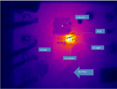
  • Change the L and C values to reduce the impedance.
  • Add damping resistors to reduce the filter impedance at its resonant frequencies (also called the Q factor). You can compare the red (undamped) and blue (damped) traces in Figure 2.

So far, I have discussed classic feedback loop instability, subharmonic oscillations and input-filter oscillations. In the next installment, I’ll look at oscillations caused by remote sensing connections.

Power topology choices for power-hungry devices

$
0
0

It is hard to choose a power topology for a wireless design when there are so many power-management integrated circuits (IC) out there. It may be hard to tell where to start, so I always start at the selection basics. The application of the design and onboard devices will determine the different voltage rails needed for operation.

Consider a smart lock or a heating, ventilation and air conditioning (HVAC) damper control system. This control system usually consists of a higher-voltage motor driver than the rest of the board The lower-voltage rail powers the MCU, radio and other sensing components.

A power management IC will make creating the different voltage rails easier. In the smart damper system, you have two ways to create two different voltage rails. The first option is to create the 3V rail with the batteries and then boost the voltage up to 6V for the motor driver. The second option is to have the batteries supply the 6V for the motor driver and then step the voltage down to 3V for the rest of the system.

The next step in the design is to choose a power topology. Three main power topologies are possible for smart damper applications: low dropout (LDO) regulator, step-down converter (also known as buck) and boost (see Figure 1). The LDO and buck implementations are not event-dependent, meaning that the two topologies use the same amount of energy regardless of how many damper louver movements occur in a day. The LDO and buck will drop the voltage down to generate the lower-voltage power rail to run the microcontroller (MCU), and the higher-voltage components run off the higher battery voltage. The boost is event-dependent because each damper adjustment event must boost up the voltage from 3V to 6V for motor and light-emitting diode (LED) operation.

Figure 1: Power topologies

I chose a buck configuration because the LDO has ground leakage current, whereas the buck has zero ground leakage current and therefore more efficiency.

For more analysis into power topologies for smart lock and HVAC damper systems, check out our reference design guides. The Smart Lock Reference Design Enabling 5+ Years Battery Life on 4x AA Batteries and Smart Damper Control Reference Design With Pressure, Humidity and Temperature Sensing both include more in-depth analysis into the various power topology choices.

Skipping ahead to the part choice, I chose the TPS62745 step-down converter because of the extra benefits it offers for low-power designs. This device has select lines that enable users to select the output voltage, and therefore removes the need for a feedback resistor, thus slightly decreasing bill of materials (BOM) cost. The TPS62745 can dynamically enable or disable the battery voltage check with the use of an enable pin and an external resistor voltage divider. Energy is conserved because the voltage divider is only enabled when a battery voltage check is necessary. The rest of the time, the divider circuitry does not use energy and is not connected. The TPS62745 is also efficient at extremely light loads; it is 85% efficient at 10μA. Efficiency is key because the smart damper systems are asleep much of the time.

Figure 2: Smart damper reference design block diagram

With your power topology and management IC chosen, all you have to do now is select the parts and sensors that connect to each of the power rails. TI has a wide selection of power-management ICs and different flavors of MCUs to suit your system needs.

Additional resources

Another chance to catch the 2016/2017 Power Supply Design Seminar

$
0
0

For nearly four decades, the Texas Instruments Power Supply Design Seminar has brought in-person training from power-supply experts directly to customers.

For each seminar, we carefully choose topics under guidelines set by Bob Mammano. Ultimately, each topic selected must be useful, educational and interesting. We take pride in the fact that the seminar is not a sales pitch, but truly an educational experience.

Our most recent 2016/2017 seminar was the 22nd edition (SEM2200), which wrapped up earlier this year after touring the United States, China, India, Japan, Taiwan, Korea and Europe. Personally, I am thankful to have been a part of the seminar tour, and to have had the opportunity to meet so many fellow engineers in the power-supply community.

If you missed the last seminar tour, it’s not too late; we are now preserving the experience for you online through a new training site, with all of the 2016/2017 seminar material in one place. With a myTI login, you can access videos of each presentation and downloadable versions of the papers and presentation material. Each video has been studio recorded and is around 40 minutes in length.

SEM2200 includes seven topics covering a variety of power-supply-related issues, written by expert engineers with practical experience dealing with those topics. They are:

  • Design of a high-frequency series capacitor buck converter” by Pradeep Shenoy. In this paper, Shenoy introduces the series capacitor buck-converter topology and discusses how it can significantly reduce the size of point-of-load (POL) voltage regulators. He also covers the limitations of conventional high-frequency buck converters and how the series capacitor buck converter overcomes these challenges.
  • Flyback transformer design considerations of efficiency and EMI” by Bernard Keogh and Isaac Cohen. The flyback converter is widely used in AC/DC power supplies due to its simplicity and wide operating range. In this topic, Keogh and Cohen focus on the importance of transformer design, since this single component has an enormous impact on converter efficiency and electromagnetic interference (EMI) performance.
  • Switch-mode power converter compensation made easy” by Bob Sheehan and Louis Diana. Compensating power supplies can be an arduous task for those not well versed in it. Sheehan and Diana break down the procedure into a step-by-step process that you can easily follow to compensate a power converter, while also explaining the theory of compensation and why it’s necessary.
  • Bidirectional DC/DC converter topology comparison and design” by Zhong Ye and Sanatan Rajagopalan. A bidirectional DC/DC converter is a key element of many new applications, such as automotive, server and renewable-energy systems. For this topic, Ye and Rajagopalan use a 48V/12V bidirectional converter as an example with which to revisit the hard-switching synchronous buck topology and compare it to a transition-mode totem-pole zero-voltage-switching (ZVS) topology.
  • SiC and GaN applied to high-frequency power” by John Rice and Rais Miftakhutdinov. Emerging wide-bandgap (WBG) silicon carbide (SiC) and gallium nitride (GaN) power devices are steadily gaining popularity in power electronics and have the potential to significantly increase a power converter’s efficiency and power density. In this paper, Rice and Miftakhutdinov examine important design issues when using WBG devices including drive technique, mitigating layout and packaging parasitics, high-frequency measurements, and simulations.
  • Under the hood of a noninverting buck-boost converter” by Vijay Choudhary, Timothy Hegarty and David Pace. When it comes to designing buck-boost converters, there is a huge gap between the simple inverting buck-boost converter in textbooks, which actually produce a negative output voltage, and real-world buck-boost applications that require a positive output. With this paper, Choudhary, Hegarty and Pace fill a gap in buck-boost literature by presenting various topologies used in noninverting buck-boost designs.
  • Design review of a 2-kW parallelable power-supply module” by Roberto Scibilia. In this paper, Scibilia steps through the design procedure of a real project that resulted in a prototype for a 2kW power-supply module. He covers the selection of the main power stages, including a continuous conduction mode (CCM) power-factor-correction circuit and a peak current mode-controlled isolated DC/DC resonant phase-shifted full-bridge converter with synchronous rectification.


I hope that you find the material from the seminar series truly useful, educational and interesting. Please share your questions and thoughts on the SEM2200 topics or the seminar in general by commenting on this post. Of course, as we are busy preparing for the next seminar series, we are very interested to hear what topics you would like to learn more about as well.

Decoding power module derating curves

$
0
0

As electronics get smaller and smaller, power-supply designers must consider thermal limits when designing their power supplies. A smaller power supply is not useful if it cannot operate at a heavy load inside a specific application environment, which includes the ambient temperature.

One common thermal limit is represented in a derating curve, which you’ll find in most power-module data sheets. The derating curve shows the amount of drawable current or power at various ambient temperatures, while still keeping the power module within its temperature specification (usually below 125°C). Figure 1 shows two such curves from the 2A TPS82140 power-module data sheet.

Figure 1: Derating curves for the 2A TPS82140 power module

As Figure 1 illustrates, derating curves change slightly with changes in input and output voltage, so it is important to look at the appropriate curve for a given design. Generally, derating gets slightly worse as the output voltage increases, because the total output power – and thus the total power losses – are higher. This is counter-balanced by the efficiency, which tends to increase with increasing output voltage, and helps reduce the power loss. Finally, derating curves are based on a specific printed circuit board (PCB), which is usually the power module’s evaluation module (EVM). Unlike the Joint Electron Device Engineering Council (JEDEC) test PCB, the EVM more closely reflects a real-world design.

Pin-to-pin and drop-in compatible with the 3A TPS82130, the 2A TPS82140 and 1A TPS82150 offer much better derating performance, which reduces the power-supply designer’s headaches. Even with a 5V output, the TPS82140 safely gives its full 2A current up to a very balmy 65°C. Figure 2 shows the lower-current TPS82150 supplying its full 1A current up to 95°C. Even here in Texas in the summer, that is downright hot!

Figure 2: Derating curves for the 1A TPS82150 power module

Of course, to get the derating performance shown in the data sheet requires a decent PCB layout. But with just five external passives and a total solution size of about 42mm2, a good PCB layout is easy to accomplish.

An easy-to-design, small power module that gets its heat out. Where can you use it in your circuits?

Additional resources


Create a power supply for a MRI application

$
0
0

Magnetic resonance imaging (MRI) uses a large magnet and radio waves to look at organs and structures inside your body. There are a number of challenging design requirements when designing a power supply for MRI applications. Because of the sensitivity of the measurements made by an MRI machine, the oscillator frequency of the power supplies needs to be precisely placed at a frequency that will not corrupt the MRI image.

The switching frequency of the power supply must be synchronized to a 2.488MHz clock because as the MRI is scanning, it radiates a high magnetic field, typically in the range of 1-3 Tesla. Because traditional magnetic-core materials used in power supplies would saturate under such levels, air-core inductors replace the magnetic cores. However, for an inductor having no ferromagnetic core material, the air-core approach provides very low inductance values.

One solution to the MRI power supply is the LM5140-Q1, an automotive-qualified dual-channel synchronous buck controller. One of the features of the LM5140-Q1 that make it desirable for a MRI application is its ability to be synchronized to an external clock up to 2.6MHz.

The LM5140-Q1 works in many nonautomotive applications because it solves certain specific design challenges. For example, since the device operates at 2.488MHz, you can use it in an MRI power supply.

MRI inductor design steps

The inductance required for an MRI power supply is proportional to the switching frequency, as shown in Equation 1:

where L is inductance in microhenries, VOUT is the output voltage, ΔI is the inductor ripple current, FSW is the switching frequency and D is the duty cycle.

Once you have calculated the required inductance, you can use Equation 2 to determine the air-core inductor size:

where L is inductance in microhenries, d is the coil diameter in inches, I is the coil length in inches and n is the number of turns.

Looking at Equations 1 and 2, you can see that a higher switching frequency will result in a lower inductor value. A lower inductance value yields a smaller air-core inductor.

An alternative to the LM5140-Q1 is the LM5141 controller. The LM5141 is the commercial single-channel equivalent of the LM5140-Q1, and has the same features as the LM5140-Q1.

Table 1 lists the typical power-supply requirements for MRI equipment. The highest power rail is 12V at 20.5A, from a 48V (nominal) input. The combination of metal-oxide semiconductor field-effect transistors (MOSFETs) RDS(ON) and switching losses (which dominate MOSFET losses when operating at 2.488MHz) make thermal management extremely challenging.

The solution is to replace the MOSFETs with gallium nitride (GaN) FETs. GaN FETs provide significant efficiency improvements over MOSFETs because they have nearly zero reverse recovery, lower RDS(ON) and a lower gate charge (QG), reducing the losses to a more manageable level. GaN FETs have critical gate-drive requirements, so the LM5113 GaN FET driver is also necessary.

VIN

(V)

FSW

(MHz)

VOUT

(V)

IOUT

(A)

46-50

2.488

3.3

7.2

46-50

2.488

5

0.6

46-50

2.488

8

20.5

46-50

2.488

12

20.5

46-50

2.488

15

2.4

46-50

2.488

-8

15.84

46-50

2.488

-15

15.84

Table 1: MRI power rails

One of the more challenging design requirements for MRI applications is the need for a negative output voltage at high output currents. This presents another challenge to overcome. In Table 1 are the power requirements for an MRI inverting buck-boost power supply, 48V to -15V (and 48V to -8V), at 15.84A. The inverting buck-boost topology transfer function (Equation 3) requires the LM5140-Q1 to be able to withstand VIN + VOUT, 50VMAX + 15V = 65V.

The LM5140-Q1 is able to operate with an input voltage of 65V (70V absolute maximum), overcoming the danger of overvoltage stresses.

Summary

The most valuable capability of the LM5140-Q1 controller in the context of MRI applications is its ability to be synchronized at 2.488MHz, reducing the size of the air-core inductors and keeps the switch-mode power supply switching frequency outside the sensitive ranges of MRI equipment. This allows for accurate processing of the measured signals in MRI equipment, which is the key to obtaining high quality images.  TI offers a wide variety of products for MRI systems and equipment manufacturers, including op amps, DSPs, multi-channel high- and low-speed data converters, clocking distribution, interface, and power management.

Extra tricks to increase battery life

$
0
0

In my previous blog post, “Power topology choices for power-hungry devices,” I discussed power topology choices to help conserve battery life. Today, I want to discuss other ways to extend battery life for power-hungry designs, including different software improvements and device options.

Depending on the end-equipment characteristics, software can make or break your battery-life expectations. Wirelessly connected devices can improve their battery life by going into standby for longer periods and reporting data less often. Take a sensor-to-cloud Sub-1GHz device, for example. Environmental data such as temperature, humidity and air-purity level do not change very quickly, so a reporting interval of every 30 or 60 minutes would be sufficient. During standby, the sensors could be asleep; only the radio may have to wake up at a quicker interval period to check back into the gateway and see if the user requested fresh data.

Some end equipment has tighter restraints and cannot sleep. With smoke detectors or security devices, for example, detected smoke or breaking glass are critical events that must be reported immediately. There are a couple of tricks for improving battery life via software changes in these applications. To improve battery life, you can decrease the wireless transmit power if the install location is relatively close to the gateway. Another trick is to have the critical sensor always on while the wireless microcontroller (MCU) sleeps, waiting for an event to occur. The sensor wakes up the MCU to send out a critical event message.

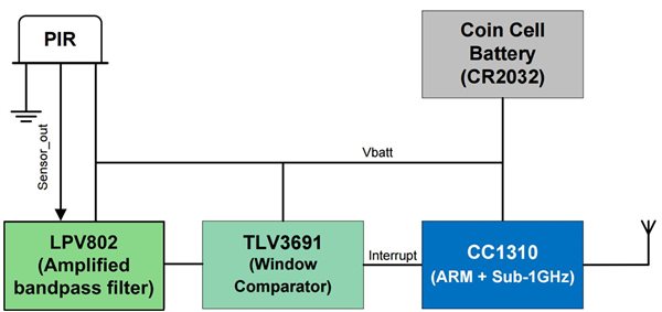
Choosing the right low-power device for your application is another way to improve battery life, but with so many devices out there, it can be hard to find the right one. I want to highlight two devices that are useful in the sensor-to-cloud ecosystem. The first is the LPV802 nanopower dual operational amplifier (op amp), which enables always-on very-low-power motion sensing in our Low-Power Wireless PIR Motion Detector ReferenceDesign Enabling Sensor-to-Cloud Networks. There are many uses for op amps, but this device is also great for smoke detectors and any application where low power is a priority.

Figure 1: Wireless passive infrared (PIR) motion detector reference design block diagram

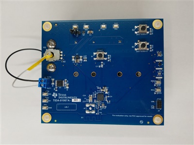
The second device that may be of interest is the DRV8833 dual-H bridge motor driver, with low-power sleep and the ability to drive two DC motors or one stepper motor. The adjustable current-limiting circuit is another nice feature of this device. You can extend battery life by avoiding unnecessary motor current from a stalled motor or other fault. Smart electronic locks, damper and actuator systems, and any small-motor applications can benefit from a low-power current-limiting motor driver.

Figure 2: DRV8833 (U3) featured on the smart damper reference design board

Texas Instruments has a couple of reference designs that use the DRV8833 motor driver. The Smart Lock Reference Design Enabling 5+ Years Battery Life on 4x AA Batteriesand the Smart Damper Control Reference Design with Pressure, Humidity, and Temperature Sensing both demonstrate the implementation of a motor-control device into a smart connected design.

I hope that some of these tips will help you achieve longer battery life in your designs. Take a look at the various reference designs I’ve mentioned here, as well as the others available on TI.com.

Additional resources:

How to correctly layout a 40A power supply: copper, vias and loop path

$
0
0

The demand for energy has gone up significantly but overall solution size continues to shrink.  To adapt, you can decrease the size of a buck converter but it must still be able to handle the increasing power consumption in the electronic system. Optimizing the layout to increase the efficiency of the buck converter will result in less electricity needed to power the system. 

Many electronic systems require several buck converters to supply power to different rails.   Some systems may need two converters or more to power a single rail with a high current demand.  The challenge of designing a smaller buck converter to satisfy this demand becomes a daunting task, but it is possible.   

New technologies and processes are now in place that enable integrated circuit (IC) designers to design buck converters that can handle up to 40A for a single output.  However, this capability introduces other issues.  One is the printed circuit board (PCB) layout.  You can design the best buck converter and power stage with space constraints in mind, but if you fail to lay out the PCB correctly, all will be lost. 

With the current at 40A per output, PCB layout is crucial in regards to heat dissipation and efficiency.  If you don’t optimize the board design, the DC loss at 40A can increase greatly due to the higher resistance of the copper-poured area.  So in this post, I’ll explain the importance of the copper-poured area, via size and quantity, and current loop path on a multi-layer circuit board.

Copper poured area

If you know the cross-sectional area of the copper (thickness × width), length and resistivity, you can calculate the resistance of the copper trace, copper plane or copper pour.  With this data, you can size the copper to optimize the PCB’s thermal, efficiency and signal-integrity performance.  A multi-layer board with multiple buried cooper planes connected with vias to the top layer or bottom layer can also help disperse the heat away from the IC. Figure #1 shows the difference in efficiency between switch-node areas.  The modified switch-node area is larger than the original, which decreases the DC loss. 

Figure 1: Modified switch node area showing a size increase vs. original switch node area

Via size and quantity

Vias make up series-resistance elements when they connect two traces or plane together.  Generally, multiple vias in parallel will reduce the effective resistance.  Just like the flat copper area and thickness, vias have a finite resistance. So you must optimize the vias’ quantity and size to optimize the thermal performance and efficiency of a converter design.

Figures #2 and #3 represent two PCBs with identical set-ups and layouts.  The only difference is the amount of vias on the thermal pad of the IC.

Figure #2: PCB with 11 vias under the thermal pad

*S2 (Site 2): Location of the integrate FET on the IC


Figure #3: PCB with 35 vias under the thermal pad         

Current loop path

You also need to optimize the path of the current loop between each alternate state of operation of the high-side field-effect transistor (FET) and the low-side FET in the buck converter.  Your optimization should include the distance and current-carrying capability of the loop.  Properly planned designs of the IC pin-outs also become a factor in the PCB layout process.  You should minimize the current-loop area as much as possible. 

As semiconductor technologies and processes continue to evolve, we are packing more silicon into the same package to enable higher current rated converter designs. Consider for example, the new 40A SWIFT™ TPS543C20 synchronous step-down converter with adaptive internal compensation and integrated NexFET™ MOSFETs.  However, the fundamental question remains of how to optimize the design so that we don’t compromise thermal performance and efficiency. Hopefully this blog helps you correctly create a smaller-sized, true 40A power supply design.


Unique techniques to increase controller power

$
0
0

The better you understand a tool, the more powerful it becomes.

One example of this is the Tektronix 576 curve tracer.  At first glance, it looks like a machine that only measures a three-terminal bipolar junction transistor (BJT) or field-effect transistor (FET).  That’s how it was advertised, so that’s what I thought until an especially talented product and failure analysis engineer showed me otherwise.  He demonstrated that this machine is really just a precise voltage and current supply with accurate measurements of both, down to the megavolts/nanoampere range.  By dynamically measuring a current-voltage (I-V) curve graphically, this tool is actually one of the most powerful circuit debugging machines in the lab.

At first I was skeptical that an old analog machine with a phosphorous cathode ray tube (CRT) monitor and mechanical switches was capable of supplying over 1kV.  My doubts didn’t last long, though, since there was soon a puzzling failure on a reliability test that we were running for a device in development, with a public announcement approaching.  Using the curve tracer, we were able to track down the root cause to intermittent pin-to-pin shorts of the quad flat no-lead (QFN) package due to board-level issues.  We shared the results with cellphone pictures of the CRT monitor; this old machine, designed for a different purpose, clearly showed the voltage collapsing momentarily as shorts between two pins formed and then fused open.

The same applies to any device used in a circuit, just because it’s advertised to work in one specific case doesn’t mean it will work well elsewhere.  While it may be easy to read the first page of a data sheet and assume that the device can only work in the specific configurations listed, that is not always the case.  One example is the maximum power of the offline converter for TI’s UCC28880 and UCC28881 switchers.  At the beginning of the datasheet a table is provided to help readers understand when which device should be used, as shown with Figure 1.

Figure 1: Power-rating table in the UCC28881 data sheet

While this table implies that 4.5W is the maximum power that this family of devices is capable of supplying when configured as a flyback, this is not necessarily the case.  The maximum power limit comes from the peak current limit (ILIMIT) of the device.  This current reaches its limit at the lowest power level at the minimum input voltage, which is 85V for a design that can support a universal input.  If the input is limited to just low line (i.e. North America, Japan) or high line (i.e. Europe, Asia), the maximum capable power level is actually higher.  While it’s obvious for high line since it has lower input currents for the same power level, low line only input requires a slight modification to the typical schematic.

This is demonstrated with 100V-450VDC, 5W, 80% Efficiency at 1W, Auxiliary Supply Reference Design for AC-DC Power Supplies.  By having a 100V DC input instead of an 85V AC input, the minimum input voltage is higher.  This enables this design with UCC28881 to have a maximum power of 5W, which is above the 4.5W maximum of the table in the data sheet.  This increase cannot continue forever though, since other limitations like thermal capability start to have an impact and can limit the operating range from reaching its theoretical capability.

Techniques like this are not limited to maximum power capability. I’ve compiled a list of reference designs that show other unique ways to bias offline power-supply controllers so that they work in conditions beyond what’s typically advertised.

Crafty idea: Create a 150V non synchronous buck solution with a lower Vin rated controller

$
0
0

Many applications today require an input-voltage rating beyond the VIN max ratings of many DC-to-DC controllers. Traditional options include using expensive front-end protection or implementing a low-side gate-drive device, which means employing an isolated topology such as a flyback converter. Isolated topologies often require custom magnetics and increase design complexity and cost compared to a nonisolated approach.

But another alternative exists that enables you to resolve the issue by using a simple buck controller with a VIN max less than the system input voltage. How is this possible?

Buck controllers typically derive a bias supply referenced from ground potential (0V) (Figure 1a). The bias supply is derived from the input; therefore, the device needs to withstand the full VIN potential. However, P-channel buck controllers have the gate-drive supply referenced to VIN (Figure 1b), because the gate-drive voltage required to turn on the P-channel metal-oxide semiconductor field-effect transistor (MOSFET) is at VGS below VIN. To turn off the P-channel MOSFET, the gate voltage simply goes to VIN (0V VGS) (Figure 2).

Figure 1: VCC bias generation for N-channel (a); and P-channel controllers (b)


Figure 2: Gate drive for a P-Channel controller

The fact that the nonsynchronous P-channel controller derives its bias supply to drive the P-channel gate in this way is a huge benefit and makes it possible to supply a virtual ground that floats above a 0V potential. For an N-channel high side MOSFET the voltage is derived from a supply that is referenced to ground.  This is charge pumped using a boot capacitor and diode to supply a gate voltage higher than its source potential of VIN.   With a P-channel high side MOSFET, things are a lot simpler.  To turn on the P-channel MOSFET, the gate potential needs to be lower than its source potential of VIN.  Therefore the supply is referenced to VIN only and not VIN and ground as described above.

Floating ground

How can you create a floating ground for the controller? It’s quite simple: by using an emitter follower. Figure 3 shows a basic implementation of such a scheme. The emitter of the P-channel N-channel P-channel (PNP) will sit at a potential that is Vbe (~0.7V) below the Zener diode voltage potential (Vz). In essence, you’re floating the controller to VIN and regulating the reference of the controller to limit the voltage between VIN and the device ground.

Figure 3: Creating a virtual ground using a simple emitter follower scheme

Output-voltage translation

There is one challenge to overcome. Because the controller is sitting on a virtual ground (Vz-Vbe) and generating a step-down output voltage that is referenced to ground (0V) potential, how are you going to translate the output-voltage signal to a feedback voltage (typically between 0.8V and 1.25V) sitting above a virtual ground? Figure 4 illustrates the challenge.

Figure 4: Schematic showing the difference in voltage potential between VOUT (referenced to 0V ground) and the feedback voltage of a controller (referenced to virtual ground)

To close the loop, you can implement Figure 5 by using a couple of matched-pair transistors. One pair sends the feedback signal to VIN; the other matched pair generates a current from VIN to a potential above the virtual ground.

Figure 5: High-level schematic of a nonsynchronous controller and feedback implementation using matched-pair transistors

Putting it all together

The LM5085 is ideal for the application I’ve described because it is a P-channel nonsynchronous controller whose VCC bias supply is referenced to VIN. The LM5085 can withstand input voltages up to 75VIN in traditional applications. For applications with input transient voltages much higher than 75V, consider the solution presented here, specified for an output of 12V.

Starting from the controller feedback voltage of 1.25V and using a current to generate the feedback (Ifb) set to 1mA, calculate the Rfb value using Equation 1:

where Rfb = 1.25k.

Rfb1 sets the reference current for the current mirrors. Once again, with 1mA as the reference current and using Equation 2, calculate Rfb1 to set the output voltage:

where VOUT = 12V, Rfb1 = 11.3k and Vbe is ~0.7V.

With 1mA flowing into Rfb2 and the emitter current being approximately equal to the collect current (Ie~Ic), this sets the reference current Iref2. The loop is closed and the voltage will regulate to the set voltage described.

Output voltage regulation

One possible application this idea is suitable for is when voltage transients are significantly higher  than the absolute maximum of the LM5085. The LM5085 is a constant on-time (COT) controller; as such, its on-time (Ton) is inversely proportional to VIN. However, when clamping the VIN to the LM5085, Ton will no longer adjust with increasing VIN (to the power stage) because the device will have a fixed voltage set by the Zener diode while the Vin to the power stage is increasing. This will cause the frequency to drop as the input voltage to the power stage increases beyond the clamping voltage to the LM5085; the regulation voltage may begin to increase slightly as a result. Therefore, take care to size the ripple-injection voltage using a Type 1 ripple-injection scheme, thus ensuring that the ripple is set within acceptable limits to maintain stability and minimize error on the output from increasing ripple.

Example schematic

Figure 6 shows an example schematic of a 48V supply with an absolute maximum VIN rating of 150V. The example board can deliver 12VOUT at 3A.


Figure 6: A 24V to 150VIN (max)/12VOUT at 3A design using the LM5085

Figure 7 shows an efficiency plot taken from a prototype board, with efficiency (%) vs. load current (A).

Figure 7: Efficiency (%) vs. load current (A) at various input voltages

Figure 8shows the switch-node voltage and inductor ripple current at 150VIN.

Figure 8: Channel 1 switch-node voltage, channel 4 inductor ripple current

Conclusion

You can use a P-channel nonsynchronous buck controller in applications where the input voltage of the system exceeds the maximum input-voltage rating of the device. This application has the benefit of using a lower-cost controller with minimal component count. For design guidance on the power stage of the buck converter, please see the application information in the LM5085 data sheet.


Viewing all 437 articles
Browse latest View live


<script src="https://jsc.adskeeper.com/r/s/rssing.com.1596347.js" async> </script>