Quantcast
Channel: Power management
Viewing all 437 articles
Browse latest View live

Design competitive USB OTG power supply

$
0
0

Universal Serial Bus or “USB” has been around for a long time; at the very beginning, USB had exclusive primary and secondary hosts. The primary data transmission was mainly from the PC and the secondary transmission was to mobile phones, mice or keyboards. With the development of consumer electronics, however, the demand for data transmission from the smartphone to the USB drive, tablets to smartphones and cameras to the printer has increased.

USB On-the-Go (OTG) is a specification that enables devices to act as either a primary or secondary host. USB OTG is widely adopted in PCs, smartphones, EPOS (Electronic point-of-sale) and power banks. The roles of primary and secondary hosts can change according to the protocol. Data can be stored in a USB drive from a smartphone or camera and the smartphone can also act as the secondary host when connecting to a PC as a primary, for example. Digital camera photos can directly upload to the printer and no longer have to be transferred by a PC. Data transfers between the “secondary” and “secondary” hosts.  It’s really amazing and useful in our daily life. Figure 1 shows a USB OTG disk and some USB OTG cables in the market.


Figure 1: USB OTG drive (left) and USB cables (right)

The OTG function is very popular in portable devices, most of which are powered from lithium-ion (Li-ion) batteries (2.7V to 4V). A boost converter is needed for USB OTG power supplies (typically 5V).

With data speeds increasing, the USB Implementers Forum has updated the power specification several times, announcing the newest USB Power Delivery (PD) specification for USB OTG devices in 2016. In this USB PD specification, the maximum current at 5V is 3A.TI’s high efficiency step-up converter, the TPS61230A, can cover most applications for this specification. For most portable devices, package size and thermal performance are critical because of the limited space inside smartphones. The TPS61230A achieves a good balance between size and performance (efficiency, thermal), and meets the maximum 5V/2.4A power demand of USB PD from the Li-ion battery, as shown in Figure 2.

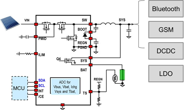
Figure 2: Block diagram for USB OTG Vbus power supply

The TPS61230A is based on a valley current-limit mode-control scheme with a 4.8A minimum switch current limit. The device integrates two low RDS(on) FETs (18mΩ/high speed, 21mΩ/low speed) which results in higher efficiency as well as good thermal performance. Only 25°C temperature rise will be achieved with VIN=3.6V, VOUT=5.0V, IOUT=2.0A under room temperature condition as shown in figure3.
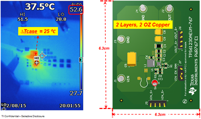
Figure 3: Thermal Performance and EVM

The TPS61230A frequency can be as high as 1.15MHz to enable small-sized inductors and capacitors. The TPS61230A is compact; the QFN(Quad-flat no-leads) 2mm-by-2mm package has only seven pins out. The enhanced power bus underneath the package facilitates thermal dissipation (the thermal resistance is 56°C/W with vias underneath the power bus). The TPS61230A is very easy to design in power systems, while the seven pins out make printed circuit board (PCB) layout very easy.

Figure 4 shows the efficiency curves with different input voltages. The TPS61230A has an excellent output capacity of 3A at VOUT = 5V and VIN = 3.6V; efficiency can be as high as 94%.

Figure 4: Test condition: VOUT = 5V, L = 1µH (XFL4020-102MEB)

In summary, thanks to the low on-resistance of both high-side and low-side MOSFET, TPS61230A can make your design more compact, much cooler but even more powerful.


Small and efficient power supply for the Altera™ MAX® 10 FPGA

$
0
0

Are you designing with Altera’s™ MAX® 10 FPGA? If so, you probably just want a small, efficient and proven power solution without having to devote much thought or design time to it. The power supply should be simple and small enough to fit on a fraction of your printed circuit board (PCB) and efficient enough to not require heat sinks or dominate your system’s thermal budget. But most importantly, the power supply must work. It must meet the requirements of the FPGA and operate within your specific system. The Small, Efficient, Easy-to-Use Power Supply Reference Design for Altera™ MAX® 10 FPGA for up to 125°C is such a proven design and provides a detailed design guide with operating waveforms and performance data, as well as the schematic, bill of materials (BOM), and PCB layout for you to implement this design in your system.


The reference design supports the dual-supply power option of the MAX 10 and contains an option which supports the Instant-On feature. The power supply supports a 6-A VCC (core) rail with the TPS62480 step-down converter and provides 2-A each for the VCCIO (for double data rate (DDR) memory) and VCCA (analog) rails with two TPS62097 step-down converters. These characteristics enable you to take advantage of the full operating performance of the FPGA and not be design-constrained by any power supply limits. The design guide contains all the necessary data and waveforms to meet the FPGA power requirements. Figure 1 shows an example of the VCCA rail meeting the 5% regulation requirement to a 50% load step with plenty of margin.

Figure 1: VCCA transient response to a 50% load step

Now that the power supply is proven to support the FPGA, how efficient and small is it? The reference design fits all three power supply rails in less than 300 mm2 of PCB space. While a smaller size is possible by using power modules, 300 mm2 is already a very small size for a discrete design that requires three different voltages.

Efficiency is important at the power supply’s full rated load but also at your full load, which may be less than the power supply’s rated current based on which FPGA functionality is used. A flat efficiency curve is important to get high efficiency at a variety of load currents. Overall for all rails combined, the TIDA-01366 achieves 89% efficiency at its full load current, but more importantly achieves 92% efficiency at half load. Figure 2 shows the efficiency of the VCC rail, which peaks at 91%. Figure 3 shows the efficiency of the VCCA rail, which peaks at 95%.

Figure 2: VCC efficiency with a 5-V input voltage 

Figure 3: VCCA efficiency with a 5-V input voltage 

High efficiency also supports operation at higher ambient temperatures. The reference design uses components which are rated to operate at 125°C. Additionally, the design includes a temperature warning flag which asserts at 120°C for an extra layer of safety. If asserted, the system then takes actions to reduce its power consumption, such as reducing the FPGA’s activity, or to decrease the system temperature, such as turning on a fan.

Small, efficient, and proven. What else do you need in your FPGA’s power supply reference design?


Precise Current Limiter for Smart E-Meter

$
0
0

Automatic meter reading (AMR) systems have become more popular in recent years. This technology saves electricity providers the expense of periodic trips to each physical location to read a meter so that billing is based on real-time consumption rather than on estimations. Because of these advantages, AMR has even become a mandatory requirement to all new generation e-meters in some countries.

Below you’ll find a typical block diagram for a smart e-meter system. Data transmission is achieved by a replaceable communication hub with hundreds of microfarad capacitance.  The communication hub is plugged in the e-meter, and its power supply comes from the e-meter’s internal AC/DC converter. If the communication hub is damaged, it must be replaced, which causes a communication hub hot plug to occur. However, the electricity monitor circuit is required to operate normally even though its power supply comes from the same internal AC/DC converter. In order to meet this requirement, a device with current limit function is necessary to connect the AC/DC converter and communication hub.

Figure 1. Smart Meter Power Topology

The TPS1H100-Q1 is a single-channel 80mΩ Rdson smart, high-side switch with full diagnostics and protection. It integrates an accurate adjustable current limit function at 20 percent tolerance across a wide temperature range between -40°C and 125°C. Because the AC/DC converter output voltage is quite stable, a precise power limit is achieved with this accurate adjustable current limit function to help save AC/DC converter power and PCB size.

Take UK smart e-meter standards as an example. The communication hub requires at least 6W power to guarantee its normal operation. To simplify the calculation, the AC/DC output voltage tolerance is neglected. If TPS1H100-Q1 is used as the current limiter, the AC/DC converter needs to leave  power for the communication hub during the design. However, if a current limiter with 40% current limit accuracy is selected; the AC/DC converter needs to leave  power for the communication hub. This example illustrates the current limit accuracy influence to AC/DC converter power margin.

The adjustable current limit accuracy of TPS1H100-Q1 is shown below in the two graphs. Figure 27 shows the current limit accuracy under 0.5A current limit, and figure 28 shows the current limit accuracy under 1.6A current limit. You see here that the device’s actual performance is much better.

Figure 2. KCL=0.5A, 13.5V

Figure 3. KCL=1.6A, 13.5V

In conclusion, a smart e-meter internal AC/DC converter can be designed with lower power capability with a precise current limiter connect behind it. This help to save system cost and size a lot. In the future, the smart e-meter size is going to be smaller, a precise current limiter would be more important in the system.

Power Tips: A simple circuit to implement smooth soft start for an isolated converter

$
0
0

Most DC/DC converters require a soft-start circuit to limit the in-rush current at startup. Although a smooth soft start is required for systems with power-on reset (POR), this is difficult for an isolated converter with a controller on the primary side and a limited duty cycle or current.

Figure 1 shows the soft start of a forward converter with a duty-cycle soft start from the primary side. The steady-state output of the converter is 12V. A 50% load current is applied at 10V, the POR threshold of the system. As soon as a load is applied, the output drops and triggers system shutdown, causing the system power cycle several times. At the end of soft start, the output overshoots 10%, which is not desirable.

Figure 1: Output of a forward converter during startup with a load applied at 10V

In this post, I will use a simple circuit to achieve a smooth soft start for an isolated converter. The circuit is applied to an active-clamp forward converter with the LM5025 as the controller. Figure 2 shows the concept of secondary-side soft start.

Figure 2: Secondary-side soft-start circuit for an isolated converter

When first applying the input, the converter output (VOUT) starts to rise. The capacitor (CSS) is charging up. The CSS charging current (ISS) flows through the resistor (RSS). When ISS is high, then VBE(on)/RSS. QSS turns on and starts to pull current from the secondary-side comp node (SEC COMP), thus reducing the duty cycle. During soft start, the error amplifier saturates and the soft-start circuit dominates the feedback loop. The converter, CSS, RSS, QSS and optocoupler form a closed loop. When the output rises to regulation, the error amplifier starts to regulate and ISS reduces. QSS turns off.

Equation 1 shows the transfer function from VOUT to the optocoupler current:

While being effective, this simple circuit might not be stable because the QSS forward gain (β) is high and varies dramatically from part to part. To stabilize this circuit, insert a gain-reducing resistor (RE) between the emitter of QSS and ground, as shown in Figure 3. Increasing RE can reduce the feedback-loop gain during startup.

Figure 3: Adding RE to stabilize the soft-start circuit

Equation 2 shows the soft-start circuit transfer function with RE:

At high frequencies, use Equation 3 as an approximation of Equation 2:

I added the soft-start circuit to the converter with these parameters:

  • CSS = 0.1µF.
  • RSS = 100kΩ.
  • RE = 1.18kΩ.

Figure 4 shows the soft-start waveform with these circuit parameters. When the system starts pulling current, the soft-start circuit stops drawing current from the COMP and the duty cycle increases quickly. The converter continues to soft start, after a minor dip caused by the load transient.

Figure 4: Soft-start waveform of the soft-start circuit shown in Figure 3

Figure 4 also shows that after the load is applied, the converter switching node (VSW) has an additional voltage spike. Figure 5 shows the zoomed-in waveform. It is obvious that the system oscillates at 9.5kHz.

Figure 5: Zoomed-in soft-start waveform with soft-start circuit

The controller in this design is a voltage-mode controller. The power stage has 180 degrees of phase drop because of the double poles. It is necessary to add a zero to improve stability; you can do this by adding a capacitor (CE), in parallel to RE. In order to add 45 degrees to the phase margin, I placed a zero at 9.5kHz, the measured oscillation frequency. With RE = 1.18kΩ, I added a 15nF capacitor.

Figure 6: Soft-start circuit with improved stability

Figure 7 shows the startup waveform with CE = 15nF. The oscillation is eliminated. The total soft-start time is 50ms.

Figure 7: Soft-start waveform with CE = 15nF

During soft start, the typical optocoupler diode current (Iopto_D) is from 1.2mA to 0.8mA. This is determined by the LM5025 and the optocoupler forward gain. With RE = 1.18kΩ, the voltage across RSS is VBE(ON) + RE× 0.8mA = 1.644V. VBE(on) = 0.7V. Thus, you can calculate ISS as ISS = (VBE(ON) + RE× Iopto_D)/RSS. ISS/CSS sets the output VOUT, dv/dt. To ensured the effectiveness of the secondary-side soft-start,  the primiary-side soft-start should be set much faster than the secondary-side soft-start as well.
Test results show the effectiveness of this simple soft-start circuit to achieve a smooth soft start for an isolated converter.
Additional resources

Buck-boost regulator benefits automotive conducted immunity

$
0
0

An automotive battery’s steady-state voltage ranges from 9V to 16V depending on its state of charge, ambient temperature and alternator operating condition. However, the battery power bus is also subject to a wide range of dynamic disturbances, including start-stop, cold crank and load-dump transients.

Each automotive manufacturer has a unique and extensive conducted immunity test suite in addition to the standardized pulse waveforms given by industry standards such as International Organization for Standardization (ISO) 7637 and ISO 16750. Table 1 identifies several undervoltage and overvoltage automotive transient profiles.

 Table 1: Automotive battery continuous and transient conducted disturbances with related test levels

 Alternator-induced noise

One particularly troublesome source of noise within the audio frequency range is an automotive alternator causing a residual alternating current on its output, leading to alternator “whine” and supply modulation issues. ISO 16750-2 section 4.4, mentioned in Table 1, describes a ripple voltage on the alternator’s output in the frequency range of 50Hz to 25kHz, with a peak-to-peak amplitude (VPP) of 1V, 2V and 4V depending on the test pulse severity level. See Figure 1.

 Figure 1: An ISO 16750-2 superimposed alternating voltage test (a); a log frequency sweep profile from 50Hz to 25kHz over a two-minute sweep duration (b)

In many vehicles, a centralized passive-circuit-protection network consisting of a low-pass inductor-capacitor (LC) filter and transient voltage suppressor (TVS) diode is used as a first line of defense for transient disturbance rejection. Automotive electronics located downstream from the protection network are then rated to survive transients up to 40V without damage. However, the required cutoff frequency of the LC filter to attenuate low-frequency disturbances makes the filter inductor and electrolytic capacitor quite large. What’s required is an active power stage that eliminates the bulky passive filter components and provides a compact and cost-effective solution for tight voltage regulation and transient rejection.

Four-switch synchronous buck-boost regulator

The benefit of a wide VIN buck-boost regulator solution lies in its high power-supply rejection ratio (PSRR), offering excellent transient dynamics to attenuate input voltage transients. With that in mind, I recently wrote an article, “Automotive front-end buck-boost regulator actively filters voltage disturbances,” that describes a high density solution for automotive applications.

Figure 2 shows the schematic of a four-switch buck-boost regulator designed to output a tightly regulated 12V rail. This solution is ideal for critical automotive functions including drive trains, fuel systems, and body and safety subsystems where loads must remain powered without glitches during even the most severe battery-voltage transients. This easy-to-use design tool streamlines regulator design and implementation for faster design-in and time to market.

Figure 2: Four-switch synchronous buck-boost solution with a wide VIN range of 3V to 36V

Figure 3a shows the buck-boost regulator’s output voltage waveform when a DC input of 9V has a superimposed sinusoidal ripple with a peak-to-peak amplitude of 1V and a frequency of 1kHz. The input ripple is attenuated by approximately 40dB. Figure 3b shows the output voltage during a cold-crank transient down to 3V for 20ms using an automotive cold-crank simulator. The four-switch buck-boost converter regulates seamlessly through the cold-crank profile.


Figure 3: Measured four-switch buck-boost converter: ripple rejection at a 9V DC input (a); cold-crank performance (b)

Summary

With its high PSRR, high efficiency and low overall bill-of-materials cost, a four-switch synchronous buck-boost like TI’s LM5175-Q1 current-mode controller offers a useful solution for mitigating transient disturbances in automotive applications. This buck-boost controller is automotive qualified to facilitate its integration into vehicular 12V single-battery and 24V dual-battery systems.

Additional resources:

Waveform audit: rabbit ears

$
0
0

What does an interning doctor diagnose if he sees symptoms he has never read about in a medical handbook? A similar question can be asked of an integrated circuit (IC) validation engineer early in his career. Indeed, like a doctor, a validation engineer is assigned to evaluate the “state of health” of an IC and to make the correct “diagnosis,” which sometimes requires a deep understanding of the device “anatomy,” combined with practical experience.

A physician may begin an examination by monitoring the patient’s heartbeat. A validation engineer of a switched-mode DC/DC converter also monitors heartbeats: the switching node. But what if the switching waveform does not look like what most textbooks show? Does that indicate some kind of device “disease,” or can the engineer interpret the state as normal?

Another Waveform Audit blog "My boost converter has an off-ramp!" already explained one surprising behavior of a switching node, so in this post I will talk about “rabbit ears” – a “symptom” occurring as small bumps during switch-node toggling.

Consider a synchronous buck converter (Figure 1) operating in continuous conduction mode. At t1 (Figure 2), the low-side switch turns off and the high-side switch turns on. From t1 to t2, the high-side switch is on and Vsw is equal to VIN (neglecting RDS(on) losses). During this time, the inductor current is increasing. At t2, the high-side switch turns off, the low-side switch turns on and the inductor current starts to flow through it. From t2 to t3, the low-side switch is on, Vsw is equal to GND (neglecting RDS(on) losses). During this time, the inductor current is decreasing. At t3, the cycle starts again.

You can find typical waveform diagrams of the switching pin and inductor current shown in Figure 2 in most literature. If you go to the lab and take measurements, however, you will see that the oscilloscope picture (Figure 3) can look a bit different – it can show “rabbit ears” on the switching node at switching moments. What causes this?

Figure 1: Simplified diagram of a synchronous buck converter


Figure 2: Waveform diagrams of the inductor current (IL) and the switching node (Vsw) of a buck converter operating in continuous conduction mode


Figure 3: Oscilloscope picture of the inductor current and switching node with rabbit ears

The secret is that the simple model shown in Figure 2 does not take into account the switching dynamics. In reality, the transition between switching phases is not instantaneous. Several nanoseconds are required to turn the transistors of the output stage on and off. To avoid cross-conduction between the switches, one should open before another starts to close. The time when both transistors are off (open) is called “dead time.”

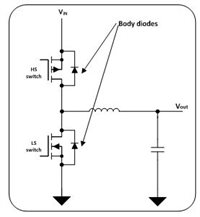
Where does the current flow when both switches are off? In fact, metal-oxide semiconductor field-effect transistors (MOSFETs) have a parasitic body diode between the drain and the source (Figure 4), so during dead time the inductor current flows through the body diode of one of the switches. Within this time, the amplitude of the switching node increases by a value approximately equal to the diode’s forward voltage drop. This increase in amplitude shows up in the switch-node waveform as a rabbit ear.

Figure 4: Simplified diagram of the output stage and output filter of a synchronous buck converter

The position of rabbit ears depends on the direction of inductor current at the moment of switching. In most applications, a buck converter sources the current. But there are applications where a buck converter should be able to sink current as well. For example, the TPS65175, a fully programmable liquid crystal display (LCD) bias IC, integrates an HVDD buck converter that can both sink and source current.

Table 1 summarizes five cases of different positions of rabbit ears for synchronous buck converters.

Table 1: Different positions of rabbit ears for the synchronous buck converter depending on the inductor current direction  


Figure 5: Conduction of the high-side body diode (a); conduction of the low-side body diode (b)

If switching nodes were heartbeats and validation engineers were physicians, they would diagnose the presence of rabbit ears as normal. Rabbit ears do lead to a slight efficiency reduction, as some energy is lost during body diode conduction. The challenge then becomes how to optimize the switching time for switched-mode DC/DC converters.

One last thing – do not mix up rabbit ears with the ringing effect described in the Analog Applications Journal article, “Controlling switch-node ringing in synchronous buck converters,” or with the switching spikes caused by bad probe techniques.

Additional resources:


Is PMBus still useful without telemetry?

$
0
0

PMBus is an Inter-Integrated Circuit (I2C)-based communication standard/interface for power-supply management. Many point-of-load (POL) converters on the market today are built with the PMBus interface, which enables digital communication between converters and their hosts. The host can be any microcontroller, microprocessor, computer, board-management controller, automatic test equipment or application-specific integrated circuit/field-programmable gate array. There are four general types of communication between the converter and host: command, control, sequence and monitor. A PMBus device can support any combinations of the above communication types.

To know which PMBus device to choose for a particular application depends on the application environment and price point. Generally, PMBus devices designed to provide monitoring functions such as input voltage, input current, output voltage, output current and die temperature have significantly higher silicon and design costs because of the addition of a precision analog-to-digital converter circuit design.

The monitoring capability through PMBus is generally referred to as “telemetry.” Figure 1 shows a graphical user interface (GUI) generated by TI’s Fusion Digital Power™ designer software. The GUI displays three telemetries: output voltage, output current and temperature.

Telemetry is also very useful in systems where data analysis and system characterization are essential. In high-reliability systems where live performance monitoring and failure analysis are absolute musts, the right kind of telemetry can provide great value.

Figure 1: TI Fusion Digital Power GUI for live telemetry reading

Even though telemetry is a very useful feature in a PMBus device, not every system or application has the right environment or the need to take advantage of the feature, especially since PMBus devices with telemetry normally cost more than devices without telemetry. But the value and benefit of PMBus is so compelling that even without telemetry, it is still worth your consideration.

One of the major benefits of PMBus is the cost savings that it brings to the overall system bill of materials (BOM). Integrating the PMBus interface into the POL converter eliminates external pin-strapping components that analog designs need to program converter configurations such as switching frequency, current limit, under voltage lockout, soft-start time, power good delay and voltage margining/tracking components.

Figure 2 shows the waveform of adaptive voltage scaling behavior by using the TPS549D22, a 40A PMBus synchronous step-down converter. A voltage identification digital (VID) chip like the TI LM10011– with several resistors to support the identical voltage scaling functionalities – is necessary to support the series of digital events shown in Figure 2. The PMBus benefit includes not only BOM cost optimization, but also the printed circuit board area reduction achieved by fewer components and routing traces.

Figure 2: TPS549D22 digital events driven by a 1MHz PMBus device

TI offers several unique high performance and high current converter families. Figure 3 summarizes TI’s PMBus and multi-chip module (MCM) converter products, including the TPS549D22, which is the highest current rated (40A) synchronous buck converter with PMBus, albeit without telemetry. Figure 4 shows the detailed PMBus command sets for the TPS549D22

Figure 3: PMBus converter selection at a glance


Figure 4: Total PMBus command sets supported by the TPS549D22

Today, PMBus is widely adopted as an effective communication means between the load and its power supply source during design, production test and every day in-system usage. Choosing the right PMBus feature for the power supply application becomes increasingly critical due to multiple considerations contributing to the success of the overall design, including functionality, performance and cost. PMBus without telemetry is still useful when it comes to configuring and controlling all the power sources, and the high integration simplifies design.

For more information on designing with PMBus, read the Power House blogs “PMBus benefits in multi-rail systems,” and “Save PCB space and overcome point-of-load design complexity with PMBus modules.”


Lightning-fast internally-compensated ACM topology – what can it do for you?

$
0
0

Internally compensated advanced current mode (ACM) is a new control topology from Texas Instruments that supports true fixed-frequency modulation and synchronization with internal compensation. Fundamentally, it is similar to emulated peak-current-mode (PCM) control, which maintains stability over a range of input and output voltages for fast transient response. What makes ACM different is that it is a ramp based, peak current mode control scheme that internally generates a ramp to achieve true fixed frequency, without using external compensation.  As well, ACM has good immunity for power-stage (inductor and capacitor) variation, but I will go into more details on the virtues of ACM here.

Why internally compensated ACM?

There are control topologies that support either true fixed frequency or pseudo fixed frequency without the need for an external compensation network. However, there are some drawbacks to using these.

Most existing true-fixed-frequency/no external compensation converters are based on traditional peak current mode, which moves the compensator from outside the package to inside the circuitry, with the internal compensator designed and optimized to cover a variety of applications. Because the internal compensation needs to cover a variety of stability ranges, the internal loop and slope compensation are very difficult to optimize if you need to achieve a fast transient response. The loop bandwidth must also be limited to accommodate wide application cases. Usually, you will see a very slow transient response, especially during large-load-current step changes.

There are also control topologies with a constant on-time modulator that maintain a pseudo fixed frequency without external compensation, like TI’s D-CAP™/D-CAP3™ control mode. The on-time is fixed for certain VIN and VOUT and the switching frequency can vary during load transient, which gives very good transient performance. However, this frequency variation also brings electromagnetic interference (EMI) concerns, especially for EMI-sensitive telecommunication applications. Internal compensated ACM addresses the drawbacks from both fixed-frequency and constant on-time control.

The simplified buck structure with ACM shown in figure 1 below feeds the feedback voltage information from the output stage to the internal integrator, with no compensation network needed externally.

Figure 1. Simplified Buck System with ACM

The simple control structure brings the benefits of:

  • A nice and easy output voltage feedback loop. It only requires RS1 and RS2 as resistor dividers to sense Vout without the compensation network, and sensed Vout information is sent back to the control loop via VFB.
  • Without external components needed for PID (proportional–integral–derivative) or PI (proportional–integral) compensation, the designer avoids the complicated compensation design, which makes it very easy to use
  • The elimination of external compensation components also saves component count and precious PCB real estate.

Internal Compensated ACM Control Overview

The overall block diagram of the ACM control loop is shown in figure 2 below.  ACM includes a voltage loop, ramp loop, comparator, current feedback and pulse-width modulation (PWM) logic.

Figure 2. ACM Control Building Blocks

Function of each block:

  • The voltage loop senses and processes error signals from VFB.
  • Ramp loop generates a ramp voltage according to VIN and PWM signal. The slope compensation is optimized to remain at half of the down slope of the ramp voltage.
  • The loop comparator adds up the input signals and terminates the PWM cycle when the sum of positive inputs reaches the sum of negative inputs.
  • Current feedback also adds DC current information to optimize the Q factor of the loop.
  • PWM logic generates the PWM signal according to the clock and output of the loop comparator.

Traditional PCM vs. Internally Compensated ACM

Table 1 shows the comparison of traditional peak current mode and Internally Compensated AMC: 

Table 1. Traditional Peak Current Mode and Internal Compensated ACM comparison

Conclusion

Internally compensated ACM control is a ramp based, peak current mode control scheme that internally generates a ramp to achieve true fixed frequency, without using external compensation.  ACM provides better transient response than traditional peak current mode by separately optimizing both the AC and DC portions of the voltage loop and ramp loop. This control mode provides an optimized solution for applications that require predictable frequency without the need for external compensation. TI’s high-performance TPS543B20 and TPS543C20 step down converters include the new internally compensated ACM control.  The converters support 25/40A with stack ability (TPS543C20 only), and include internal compensation for ease-of-use, fixed frequency for low EMI noise, and full differential sense to achieve the best VOUT set-point accuracy.

Learn more about TI’s portfolio of buck converters with integrated switches and read the “Control-Mode Quick Reference Guide” for an overview of the various non-isolated DC/DC regulator control modes offered by TI.


Comparing Bode plots in D-CAP3™ control mode

$
0
0

Converter stability is a primary requirement for any synchronous buck converter design. Confirming converter stability requires that you derive the small-signal transfer function and measure the Bode plot of a closed-loop system. It is possible to derive the small-signal transfer function rigorously using complicated mathematic equations; the results can be very insightful in terms of understanding the nature of the stability requirement. However, deriving the small-signal transfer function is outside of the scope of this post.

In the absence of theoretical analysis, you can use a network analyzer to measure the Bode plot and confirm the stability of your converter design. If done properly, the Bode plot result can be a very useful, quick way to help you gauge converter stability.

The D-CAP™ topology is gaining in popularity due to its ease of use. D-CAP stands for “directly across the output capacitor.” TI introduced a family of D-CAPTM switch mode power supplies that incorporates either the external RCC network (RRAMP, CRAMP1 and CRAMP2) or an internal ripple-injection circuit such as D-CAP3, making it easier to design with all-ceramic-output capacitor configurations (Figure 1). In this post, I will compare the D-CAP3™ Bode plot measurement results based on different setup methods, including ripple injection magnitude and small-signal injection magnitude. In order to obtain a reliable and meaningful Bode plot result, you’ll have to follow a few preliminary steps.

Figure 1: D-CAP IC with RCC network synchronous buck converter

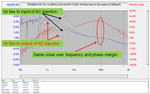
Figure 2 shows two setup methods of network analyzer equipment: the VO pin at the input (VA in Figure 2a) and output (VB in Figure 2b) of the AC injection. This VO pin is the same signal as the VO of the RCC network in Figure 1. From the Bode plot phase margin test theorem, the crossover frequency is defined when the frequency of the converter loop gain is at 0dB or unity. At this crossover frequency, the phase margin of the converter loop gain must be positive, and at least higher than 45 degrees in order to reduce output voltage ringing during the load transient step.

The results in Figure 3 show the minimum difference between the two setup methods. However, by using the results from Figure 2a, you can confirm the resonant frequency location of the inductor and output capacitor values of the converter. The results are from the TPS548B22 evaluation board with VIN =12V, VOUT =1V, FSW = 650kHz, L = 330nH, COUT = 2 x 470µF + 7 x 100µF and ILOAD = 10A resistive load.

Figure 2: Bode plot setup of VO pin at VA (a) and at VB (b) on TPS548B22 evaluation module EVM


Figure 3: Bode plot results from the setup shown in Figure 2

You might ask how the magnitude of the RCC network affects the Bode plot result. Due to the noise sensitivity of this topology, the controller requires a minimum ramp magnitude to ensure that the converter operates correctly in steady state while providing the best load-transient response. Figure 4 shows the comparison results between a 6mV and 12mV ramp magnitude of the RCC network. The crossover frequency of the 12mV ramp is around 29kHz, with a 95-degree phase margin. The crossover frequency of the 6mV ramp is about 102kHz, with a 117-degree phase margin.

Figure 4: Bode plot comparison with different ramp values on the TPS548B22 EVM

As you can see from Figure 4, the RCC ramp magnitude affects the crossover frequency and phase margin.

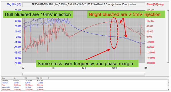
Another question that you may have when taking Bode plot measurements in D-CAP 3 control mode is what the AC injection magnitude range needs to be when measuring – and it must be a range that won’t affect the converter loop-gain result. Figure 5 shows the comparison results with a 2.5mV and 10mV AC injection signal. A good recommendation value is to keep this AC injection magnitude to 10mV or less.

Figure 5: Bode plot comparison with different AC injection magnitude

To obtain a good Bode plot result, it is critical that you pay attention to the setup and take some precautionary steps to reduce errors in the measurement. Some basic recommendations are:

  • Before taking the measurement, calibrate the network analyzer or do a 0dB measurement to ensure flat gain and zero phase across the frequency range of interest.
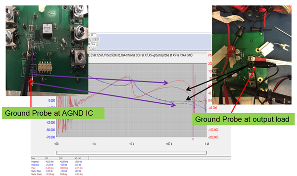
  • Use the analog ground of the controller as the reference for the Bode plot probes. See the example comparison in Figure 6.
  • Keep the probes far away from the inductor in order to avoid coupling the inductor magnetic-field signal onto the AC injection magnitude.
  • If possible, use the resistive power dissipation at the load connection instead of the electronic current source mode.

Figure 6: Bode plot comparison on customer board with different ground probe connection location

A Bode plot measurement result enables you to quickly gauge converter stability rather than deriving the converter’s small-signal transfer function. The phase margin test theorem gives the same results whether the VO pin is at the input or output location of the AC injection in D-CAP3 control mode setups. To obtain a trustworthy Bode plot result that gives you confidence about your system, take some precautionary setup steps to minimize errors.  Read the blog posts “D-CAP3 – A sequel better than the original” and “Design advantage of D-CAP control topology” for more information on TI’s D-CAP control architecture.


LDO basics: Current limit

$
0
0

The key goal of DC power management is to provide a regulated, steady voltage for the slew of electronic content present in any system. This is particularly true for low-dropout regulators (LDOs), as they can achieve a regulated voltage while supplying current as needed.

There are external conditions and scenarios where an LDO might experience an unexpected high current draw. This high current will harm most electronic systems as well as the host power-management circuit if the current is transmitted to the other electronics being powered. Selecting an LDO with internal protection from short circuits and current limiting can help prevent this harmful effect and provide additional protection when designing the overall power management.

What is current limiting/how does it work?

Current limit in an LDO is defined by establishing an upper boundary for the current supplied. Unlike a constant current source, LDOs supply current on demand but can also control the total power regulated. Current limiting is achieved through internal circuitry controlling the output stage transistors inside the LDO. See Figure 1. This is a classic current-limit circuit for an LDO and is commonly referred to as a “brick-wall” current limit due to its abrupt current stop once the limit is reached. In this internal circuit, the LDO measures the output voltage for feedback but also measures a scaled mirror of the output current against the internal reference (IREF).


Figure 1: A current-limiting internal LDO structure

Brick-wall current limiting

In a brick-wall current limit, the upper boundary is defined and the LDO supplies current incrementally until the limit current limit is reached. Once the current limit is exceeded, the output voltage is not regulated and is determined by the resistance for the load circuitry (RLOAD) and the output current limit (ILIMIT) (Equation 1

                                             (1)

The pass transistor will continue this operation and dissipate power, as long as the thermal resistance (θJA) allows for healthy power dissipation where the junction temperature is within acceptable limits (TJ< 125°C). Once VOUT goes too low and the thermal limit is reached, thermal shutdown will turn off the device in order to protect it from permanent damage. Once the device has cooled, it will turn back on and regulation can proceed. This is particularly important in cases where a short circuit may present itself, as the LDO will proceed to regulate VOUT to 0V.

For example, TI’s TPS7A16 can limit high current outputs in wide voltage conditions. Figure 2 shows an example behavior of the current-limiting function in 30V input conditions. As you can see, once the current limit is surpassed, the LDO continues to supply at the limit, but it will no longer regulate VOUT to 3.3V. Once the thermal limit is surpassed at 105mA, thermal shutdown kicks in.

This current-limiting function is helpful for charging nickel-cadmium and nickel-metal hydride single-cell batteries, as both require a constant current supply. An LDO like the TPS7A16 can help maintain a constant current at the limit (ILIMIT) as the battery voltage changes while the battery is charging.


Figure 2: TPS7A16 brick-wall currentlimiting (30VIN, 3.3VVIN, VSON at 25°C)

Foldback current limit

Foldback current limit is very similar to the standard upper-boundary limit. But the main goal of foldback current is to limit the total power dissipation, keeping the output transistor within its safe power-dissipation limit by reducing the output current limit linearly while VOUT decreases and VIN remains steady.

Devices like the TLV717P feature foldback current limiting and benefit from it, due to being predominantly offered in very small packages with higher thermal impedance. If you look at the behavior of the TLV717P’s output current limit, as shown in Figure 3, you can see that the maximum power dissipation allowed at 25°C is 150mW, as VIN is specified as VOUT + 0.5V. After the current limit is exceeded and VOUT begins to reduce (assuming a constant RLOAD), both IOUT and the power dissipation reduce. This adds a bit of complexity for non-ohmic devices that draw a constant current and could trigger a lockout condition in which the powered device continues to reduce VOUT and the LDO continues to reduce IOUT.


Figure 3: TLV717P output current limit vs. VOUT

Whenever harmful conditions may be present such as short circuits or overloading, it is important to prevent the transmission of this effect to other sensitive electronics. Protected LDOs can provide a wide range of functionality that can make any design much more robust. Read more blog posts on the basics of LDO design.

 Additional resources:


Good pin practices with buck converters

$
0
0

Many synchronous buck converter designers face a common issue: how best to connect the open drain power-good flag, also known as the power-good (PGOOD) pin. In this post, I will explore the expected behavior of power good when it is tied to various different pull-up sources. There has been some misinformation floating around that hopefully this post will clarify.

As many converter data sheets describe, the function of the PGOOD pin is to indicate high after the switcher output gets within the target regulation. For instance, when the output voltage of one of TI’s step-down regulators with integrated switchers is within +10% and -5% of the target value, internal comparators detect a power-good state and the open-drain field-effect transistor (FET) turns off, enabling the power-good signal to rise to the pull-up voltage. If the output voltage goes outside of +15% or -10% of the target value, the open-drain FET turns on and the power-good signal becomes low after a short 2ms delay. Power good will also go low (regardless of output voltage) in a few other scenarios, such as when enable goes low, in order to facilitate quick shutdown sequencing in daisy-chained systems.

The recommended pull-up for the PGOOD pin is to tie it to the internally generated VREG pin or BP pin. The output remains low when the device is disabled or not powered, which has the benefit of defining the power-good state before any bias is present. Some users with different input/output (I/O) voltages prefer to pull the PGOOD pin up to an external bias like 3.3V, which can introduce some complications due to timing. Before providing VIN/VDD (typically 12V), there is nothing powering the comparators and logic “defining” the power-good state. At this time (before applying power), the open-drain FET’s gate voltage is determined by leakages and is more likely to turn off than to turn on. Coupling that fact with an external pull-up voltage that could be present before VIN/VDD can lead to the PGOOD pin showing high during an otherwise PBAD state.

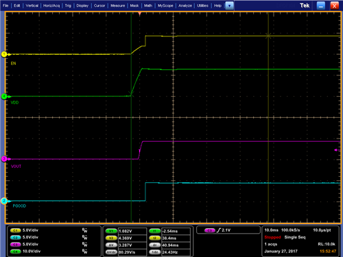
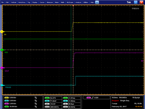
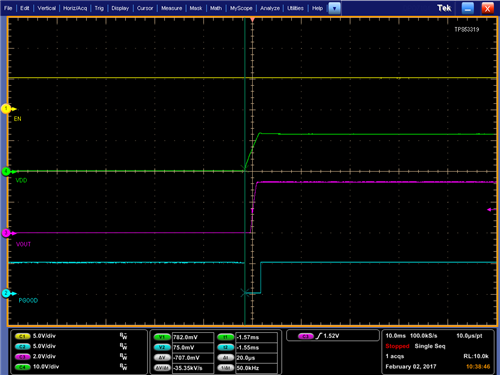
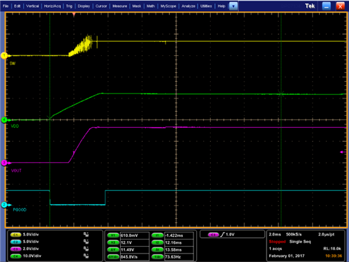
Figures 1 through 5 are scope shots of PGOOD pulled up by VREG, and PGOOD pulled up by an external voltage using the TPS53315 and TPS53319 synchronous buck converters. Note how PGOOD will float up to the pull-up voltage, even though the device is not regulating.

Figure 1: The TPS53315 power good is clean with no glitches


Figure 2: The TPS53319 power good is clean with no glitches


Figure 3: The TPS53315 power-good glitch that results in PGOOD ties to enable: enable power goes high first, then VDD


Figure 4: The TPS53319 power-good glitch that results in PGOOD ties to enable: enable power goes high first, then VDD

Figure 5: The TPS53319 power-good glitch that results in an external 3.3V pull-up on PGOOD being present before VDD/VIN

It is best to use a self-derived voltage through dividers in order to guarantee the logic state of the PGOOD pin at all times.  When using external always-on voltages, the downstream logic needs extra consideration in order to avoid a small power good glitch before the controller power supply (VDD) gets up to ~1V. Get more information on all of TI’s buck converters with power good.


How to approach a power supply design – part 2

$
0
0

In the first installment of this two-part series, I described how important it is to have a good specification for properly designing a power supply. In part 2, I will outline which parameters of your specification (see Figure 1) influence the decision for certain topologies.

Figure 1: Parameters of your specification, which can influence the decision of a certain topology

When your application does not require an isolation barrier between the input and the output, the ratio between Vin and Vout, the ripple requirements for input and output voltage, and the maximum output power will usually determine which topology you ought to choose. Buck, boost, buck-boost, single-ended primary inductance converter (SEPIC) and Zeta are the most common nonisolated power-supply topologies for power ranges up to 250W. The buck converter steps down its input voltage and the boost converter steps it up. Buck-boost, SEPIC and Zeta can have an input voltage that is equal to, smaller or greater than their output voltage. If your input voltage has a different sign compared to the output voltage, the inverting buck-boost or Cuk converter should be your choice. For both topologies, the absolute value of the input voltage can be equal to, smaller or greater than the absolute value of the output voltage.

Table 1 lists the relationship between input voltage and output voltage and the typical power range for the nonisolated topologies I’ve mentioned. If your application needs more than the output power limit shown in Table 1, it might make sense to parallel two or more interleaved converter stages or use an isolated topology (see Table 2), because these are already intended for greater power levels.

Table 1: Overview of nonisolated topologies

Isolated topologies can step their input voltage up or down. The output voltage can be positive or negative. By adding extra transformer windings, it is also possible to generate more than just a single output voltage. Flyback, forward, push-pull, half-bridge and full-bridge converters are the most common isolated topologies. The most common way to minimize losses for these topologies is to have the converters operate in a resonant or quasi-resonant mode. Resonant converters take advantage of zero voltage switching (ZVS) or zero current switching (ZCS). Examples are quasi-resonant flyback, active clamp flyback or forward, inductor-inductor-converter (LLC) half-bridge and phase-shifted full-bridge. Table 2 shows the power ranges for different isolated topologies. 

Table 2: Overview of isolated topologies

If very thorough load transients can occur at the output of your converter, it is important to know that good dynamic behavior is not possible with a flyback topology operating in continuous conduction mode, as the right half plane zero (RHPZ) in the converter’s transfer function will typically limit the bandwidth to frequencies below 5kHz for this type of converter. The bandwidth of the opto-isolator, which is usually necessary for the output voltage feedback path of isolated topologies, can be another drawback for transient response behavior. If your power supply really needs very good transient response behavior, but you have to use a different topology than a buck converter, a two-stage approach might be your best option. Another option is placing the controller on the power supply’s secondary side.

The buck, boost, SEPIC and flyback topologies are suitable for power factor correction (PFC) circuits. The most common choice is PFC boost.

In the next installment of this series, I will cover buck, boost and buck-boost converters.

Additional resources

A simple and efficient LED driver for video surveillance cameras

$
0
0

Video surveillance security monitoring is in demand, and the technology has also become more affordable for both personal and commercial use. Compelled by the need for better security, millions of security cameras have been installed worldwide.

Because many security cameras are on all the time, it is no surprise that surveillance camera manufacturers have moved to energy-saving light-emitting diode (LED) lighting. Compared to previous incandescent/fluorescent lamps, LEDs provide 80-90% more efficiency, with lower heat dissipation. LEDs also have a longer life span and require less space when implemented in video surveillance cameras.

With volumes ramping up, camera makers have clamored for LED driver board designs to be more simple, more compact and cost less. But at the same time, they need the LED drivers to have high efficiency for lower power consumption, and higher accuracy for better image resolution. Given these challenges, hardware engineers need an LED driver solution that checks off all of these requirements.

TI’s TPS54200 is a new DC/DC synchronous buck LED driver that helps support video surveillance and other end equipment. The device offers an efficient and cost-effective solution with high analog dimming accuracy. The TPS54200 is available in a simple small-outline transistor (SOT)23-6 package, enabling users to easily design LED driver boards.

Figure 1 shows a simplified schematic of the TPS54200 driving a series of white LEDs with the absolute lowest amount of external components. It would be a great solution for video surveillance cameras or other general-purpose LED lighting for commercial/industrial use.

Figure 1: Simplified schematic of the TPS54200

The TPS54200 has low RDS(on) for high efficiency when driving LEDs in strings. Flip-chip-on-lead (FCOL) technology minimizes inductance and resistance between the die and the package leads. With its low on-resistance, the device is able to operate with high efficiency (96% peak efficiency) and keep surveillance camera power consumption as low as possible. See Figure 2.

Figure 2: TPS54200 efficiency at a 1A load

TI designed the analog dimming function of the TPS54200 to have very good accuracy, which enables the current running through the LED to be proportional to the pulse-width modulation (PWM) duty ratio with excellent linearity. Pls. refer to Figure 3 Thus, you can make the microcontroller unit (MCU) generate PWM pulses with higher accuracy than typical dimming through a DC voltage.

Figure 3: 100% linearity of LED current against PWM duty

With the TPS54200, it’s possible to drive a series of LEDs at an exceptionally high brightness accuracy through the PWM input – even at a 5% PWM duty ratio. This is a huge benefit for end-equipment designers who would like to ensure accurate brightness control, even when using untrimmed LEDs for a lower-cost implementation. See Figure 4.

Figure 4: TPS54200 LED current accuracy test with untrimmed white LEDs

In keeping with the current global trend of moving to LED lighting for better power consumption, the TPS54200 can drive a series of white LEDs in a simple, easy-to-use and cost-effective design with high brightness control capability. Video surveillance camera makers and other end-equipment manufacturers that need a simple LED driver for series LED lighting would appreciate such a solution.  Get more information on designing video surveillance cameras.

Power Tips: How to upgrade a legacy power bank to USB Type-C™

$
0
0

With more and more portal devices adopting the USB Type-C™ connector, designing a power bank capable of charging these devices is suddenly a big deal. Unfortunately, the USB Type-C connector is a totally new type of USB connector. Understanding the differences between a USB Type-C power bank from legacy USB power banks is critical for successful product migration.

There actually is not much difference between a USB Type-C power bank power stage and a legacy power bank power stage. The key difference is in how the power path connectivity and device attach/detach detection is handled “From” and “To” the Type-C connector.

In a legacy power bank there is always an input charging port (such as Micro USB) and one or more output discharging ports (such as USB Type A). A battery charger inside the power bank connects to the input port. A DC/DC converter, mostly a booster, is located at the output path. Figure 1 shows this block diagram.

Figure 1: A legacy power bank

Pin connections

The USB Type-C connector is designed for higher power and higher data transmission speeds and has a nonspecific orientation. Its pin assignment has significantly improved from the USB Type A or USB Type B ports.

Figure 2 gives the pin assignments for a full-featured USB Type-C receptacle. There are 24 pins, including several new pairs. However, power bank being a dataless system, it is not necessary to consider the USB 3.1 pins and SBU pins. However D+/D- pins are needed to support BC1.2 and third party proprietary brick IDs. Use below example for connecting Type-C receptacle pins.

  • VBUS and GND: there are four pins defined for each net, respectively. Connect all of the pins in same function to share the current.
  • D+/D-: Same definition as USB Type A and USB Type B: these are used to transmit the handshake message between power bank and external device.  Two pairs are defined in a USB Type C connector but only one set would be connected to the cable. Connect the two pins in same definition directly.
  • CC: this is a new channel configuration (CC) pin used for the discovery, configuration and management of connectors across a USB Type-C cable. Connect it to a USB Type-C controller.

Figure 2: USB Type-C receptacle pin assignments

Adding VBUS switches

A USB Type-C port is configurable as dual-role port (DRP). A USB Type-C DRP power bank  one can charge or discharge via the same USB Type-C port. This will require the addition of a VBUS switch at the USB Type-C receptacle to separate the charger power path and output DC/DC power path, as shown in Figure 3.

A VBUS switch is typically configured as a back-to-back structure so that it can block the energy flow bidirectionally. When the USB Type-C power bank is connected to an adaptor, the VBUS switch on the charging path can be turned on so that the battery can be charged. If the external device is a cellphone, the VBUS switch on discharging path will be turned on while the VBUS switch on charging path is disabled. Generally, a VBUS switch also has three main purposes:

  • It can help block energy from the battery to VBUS. The output DC/DC could be a boost converter, which means that the battery voltage can go to the output through its rectifier diode. Using this VBUS switch can block the voltage applied to VBUS before attachment.
  • In a USB Type-C power bank, the valid VBUS voltage and current may vary dynamically. You can turn the VBUS switch off if an overcurrent or overvoltage event occurs at the VBUS to protect the post circuit.
  • With a USB Type-C DRP power bank, the DC/DC converters for charging and discharging connect to the same port, which requires separating the bulk capacitors for each converter in order to meet the USB Type-C’s requirements for source or sink. The bulk capacitance for a sink is within 1~10uF to limit the input rush current, while the bulk capacitance for a source should be higher than 10uF to keep the VBUS voltage stable.

Figure 3: A USB Type-C power bank with VBUS switch

Attachment event detection

A traditional power bank can detect the VBUS voltage and current to activate the microcontroller (MCU) once an attach/detach event occurs. With the new USB Type-C port, the traditional detection circuits are out of action. The CC line in a USB Type-C connector takes this responsibility. I recommend a Type-C DRP controller such as TUSB320 to implement port attach/detach events in a type C power bank. The built-in CC detection circuit in TUSB320 connects the CC line to its internal voltage source through a pull-up resistor or a current source when configured to source power. The USB Type-C controller will connect the CC to ground via a pull-down resistor when sinking power. Once there is a connection between two devices, the CC line voltage will change. The internal circuit in both devices will detect this voltage variation and start attachment event detection, as shown in Figure 4.

Figure 4: CC event-detection circuit

In summary, with a clear understanding of the pin connections, VBUS switches and attachment event detection, you can easily upgrade a legacy power bank to support USB Type-C devices.

Additional resources

Check out these TI Design reference designs:

Powering the Intel® Arria 10 GX FPGA with a PMBus Multiphase Buck DC/DC Converter

$
0
0

Field-programmable gate arrays (FPGAs) are increasingly complex system-on-chips (SoCs) that include not just programmable logic gates and random access memory (RAM) but also analog-to-digital converters (ADCs); digital-to-analog converters (DACs); and programmable analog features and signal-conditioning circuits that enable high-performance digital computations in servers, network-attached storage (NAS), enterprise switches, oscilloscopes, network analyzers, test equipment and software-defined radios.

The Intel® Arria 10 SoC is such an FPGA. TI has a fully-compliant Arria 10 GX power solution in our reference design library. Arria 10 devices are the only high-performance FPGAs and programmable SoCs developed on Intel’s 14nm Tri-Gate process, offering up to 70% lower power compared to the previous generation.

To reduce power, a Smart Voltage ID (SmartVID) interface offers a large number of very small voltage-reduction steps that are programmable into the FPGA’s nonvolatile registers in order to reduce the power dissipation of the chip.

The SmartVID feature compensates the process variation by narrowing the process distribution using voltage adaptation. Instead of a constant voltage, SmartVID-enabled devices opportunistically adjust the device voltage for optimal power – while at the same time meeting performance goals. To save power, Smart VID reduces the voltage on devices with performance beyond the specification requirements.

SmartVID enables the FPGA core power regulators to provide Arria 10 devices with lower VCC and VCCP voltage levels in a closed loop system while maintaining the performance of the specific device speed grade. These voltages can vary between 0.83V and 0.975V, in 5mV, 10mV, or 15mV increments.

When using SmartVID, Arria 10 devices must be powered up to a default voltage level for both VCC and VCCP. The VCC and VCCP rails will first wake up to a default voltage of 0.9V. After determining the voltage ID value and communicating this value to the external voltage regulator, the VCC and VCCP voltage values will change according to the determined VID value. Typically they will vary from 0.85V to 0.9V (For more information, see Intel AN11 Application Note)

One of the SmartVID communication interface options between the Arria 10 FPGA and the external Vcore voltage regulator is the two-wire PMBus digital serial interface at a 400kHz clock speed as described in Intel’s “AN711 Application Note: Power Reduction Features in Intel Arria 10 Devices”. In a PMBus system, the Arria 10 FPGA acts as a PMBus master or a slave – whatever you prefer.

If the Arria10 is the PMBus master, it will communicate the new Vcore value via PMBus to the Vcore voltage regulator (acting as the PMBus slave) in a range between 0.83V and 0.975V using the standard PMBus command “VOUT_COMMAND” – 21h hex code. The PMBus master uses the VOUT_COMMAND instruction in the data format retrieved from VOUT_MODE to write voltage ID values to the voltage regulator. The PMBus Vcore regulator will then set its output voltage to the new commanded value as dictated by the FPGA with a resolution of 5mV, 10mV, or 15mV depending on the power reduction required. Table 1 lists the SmartVID power requirements.

Table 1: Smart VID regulator requirements (source: “Arria 10 handbook”)

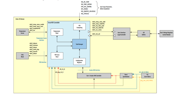
Figure 1 shows the Smart VID implementation with the external Voltage Regulato

Figure 1: Arria 10 FPGA Smart VID interface with external Voltage Regulator: “Smart VID Controller IP Core User Guide"

The regulator(s) must meet the static, ripple and dynamic power tolerances listed in the “Arria 10 GX, GT, and SX Device Family Pin Connection Guidelines” during all phases of power delivery after reaching the boot voltage. The VCC and VCCP voltage regulator supply tolerance is ±30mV.

To implement SmartVID with PMBus, you must enable PMBus in the FPGA with Quartus Prime software version 15.1. Only the Arria 10 VCC and VCCP (core) rails can use SmartVID.

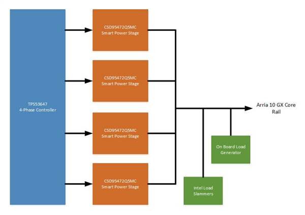
Figure 2 shows the TIDA-01419 reference design power delivery to the Arria 10 GX FPGA (10AX115U145IVG part number with high utilization) VCC and VCCP rails via the PMBus SmartVID interface.

Figure 2: Intel Arria 10 GX (10AX115U145IVG part number with high utilization) power solution with SmartVID PMBus implementation for VCC/VCCP rails - TIDA-01419 reference design


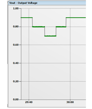
Figure 3: Intel Arria 10 GX TIDA-01419 reference design Smart VID adjustment via PMBus


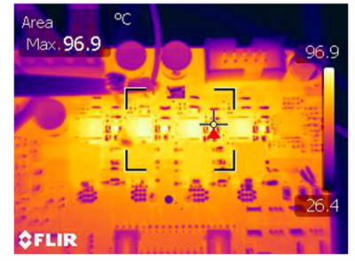
Figure 4: Intel Arria 10 GX TIDA-01419 reference design thermal performance (25degC ambient temperature, no airflow, no heatsinks, 12-Volts Input, 0.9-Volts/100-Amperes

The TI Arria 10 GX TIDA-01419 reference design uses the TPS53647 4-phase, driverless, PMBus, pulse-width modulation (PWM) controller with capability for up to 4-phase operation. The controller utilizes DCAP+™ control mode for ultra-fast load transient response, very easy loop compensation, and excellent stability irrespective of input voltage, phase count, or load current. It offers extensive parameter pin-strapping, and PMBus programming, control and monitoring of input/output voltage, current, temperature and power, as well as system faults. Since input and output power are monitored real-time, instantaneous efficiency calculations of the high-current VCC/VCCP rails can be performed.

The TPS53647 is paired with TI’s CSD95472 smart power stages, which include high-performance NexFET™ gate drivers and high- and low-side NexFET power MOSFETs stacked on top of each other in a PowerStack™ packaging configuration for high efficiency, optimal thermal performance, easy heat sinking and high power density. The smart power stages include temperature-compensated, bi-directional current sensing for reducing inductor size and cost per phase. The PowerStack™ package employs a single large GND pad on the bottom of the IC for easy top-layer printed circuit board (PCB) layout, and direct thermal sinking into the PCB internal ground planes for excellent multiphase converter thermal performance.

The TPS53647 is a pin-to-pin device to the TPS53667 6-phase controller which is also available in case a higher-phase-count design is needed to manage the thermals even better and reduce the capacitor and inductor size.

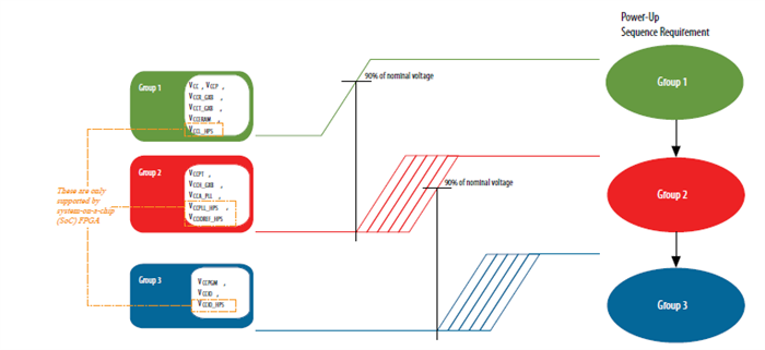
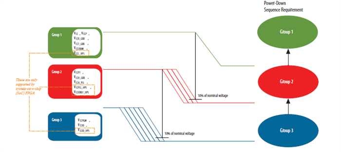
According to the Arria 10 GX documentation “A10 handbook, page 317” power up and down sequencing is needed.

Figure 5: Intel Arria 10 GX power up and down sequencing, Arria-10/a10_handbook.pdf

TI has a complete family of PMBus sequencers with monitoring, margining, and Blackbox logging that can be used as companion devices to the Arria 10 GX multiphase buck dc-dc converter.

So if you are designing with Intel’s Arria 10 GX FPGAs and looking to implement SmartVID via PMBus, consider TI’s PMBus multiphase DC/DC and sequencer solutions for the VCC and VCCP rails.

Additional resources

Source: Intel Corporation (www.Intel.com)


LDO basics: noise – part 1

$
0
0

In another LDO basics blog post, I discussed using a low-dropout regulator (LDO) to filter ripple voltage arising from switched-mode power supplies. This isn’t the only consideration for achieving a clean DC power supply, however. Because LDOs are electronic devices, they generate a certain amount of noise of their own accord. Selecting a low-noise LDO and taking steps to reduce internal noise are integral to generating clean supply rails that won’t compromise system performance.

Identifying noise

The ideal LDO would generate a voltage rail with no AC elements. Unfortunately, LDOs generate their own noise like other electronic devices. Figure 1 shows how this noise manifests in the time domain.

Figure 1: Scope shot of a noisy power supply

Analysis in the time domain is difficult. Therefore, there are two main ways to examine noise: across frequency and as an integrated value.

You can use a spectrum analyzer to identify the various AC elements at the output of the LDO. (The application report, “How to measure LDO noise,” covers noise measurements extensively.) Figure 2 plots output noise for a 1A low-noise LDO, the TPS7A91.

Figure 2: Noise spectral density of the TPS7A91 vs. frequency and VOUT

As you can see from the various curves, output noise (represented in microvolts per square root hertz [μV/ Hz]), is concentrated at the lower end of the frequency spectrum. This noise mostly emanates from the internal reference voltage but also has contributions from the error amplifier, FET and resistor divider.

Looking at output noise across frequency is helpful in determining the noise profile for a frequency range of interest. For example, audio application designers care about audible frequencies (20Hz to 20kHz) where power-supply noise might degrade sound quality.

Data sheets commonly provide a single, integrated noise value for apples-to-apples comparisons. Output noise is often integrated from 10Hz to 100kHz and is represented in microvolts root mean square (μVRMS). (Vendors will also integrate noise from 100Hz to 100kHz or even over a custom frequency range. Integrating over a select frequency range can help mask unflattering noise properties, so it’s important to examine the noise curves in addition to the integrated value.) Figure 2 shows integrated noise values that correspond with the various curves. Texas Instruments features a portfolio of LDOs whose integrated noise values measure as low as 3.8μVRMS.

Reducing noise

In addition to selecting an LDO with low noise qualities, you can also employ a couple of techniques to ensure that your LDO has the lowest noise characteristics. These involve the use of noise-reduction and feed-forward capacitors. I will discuss the use of feed-forward capacitors in my next blog.

Noise-reduction capacitors

Many low-noise LDOs in the TI portfolio have a special pin designated as “NR/SS,” as shown in Figure 3.

Figure 3: An NMOS LDO with an NR/SS pin

The function of this pin is twofold: it’s used to filter noise emanating from the internal voltage reference and to slow the slew rate during startup or enable of the LDO.

Adding a capacitor at this pin (CNR/SS) forms an RC filter with internal resistance, helping shunt undesirable noise generated by the voltage reference. Since the voltage reference is the main contributor to noise, increasing the capacitance helps push the cutoff frequency of the low-pass filter leftward. Figure 4 shows the effect of this capacitor on output noise.

Figure 4: Noise spectral density of the TPS7A91 vs. frequency and CNR/SS

As Figure 4 shows, a greater value of CNR/SS yields better noise figures. At a certain point, however, increasing the capacitance will no longer reduce noise. The remaining noise emanates from the error amplifier, FET, etc.

Adding a capacitor also introduces an RC delay during startup, which causes the output voltage to ramp at a slower rate. This is advantageous when bulk capacitance is present at the output or load and you need to mitigate the in-rush current.

Equation 1 expresses in-rush current as:

                        (1)

In order to reduce in-rush current, you must either lower the output capacitance or lower the slew rate. Fortunately, a CNR/SS helps achieve the latter, as Figure 5 shows for the TPS7A85.

Figure 5: Startup of the TPS7A85 vs. CNR/SS

As you can see, increasing CNR/SS values results in longer startup times, preventing in-rush current from spiking and potentially triggering a current-limit event.

Summary

Low-noise LDOs are critical to ensuring a clean DC power supply. It is important to both select an LDO with low-noise properties and implement techniques to ensure the cleanest output possible. Using an NR/SS capacitor has two benefits: it enables you to control the slew rate and filter reference noise. For more insight on LDOs, check out other blogs in the LDO basics series.

Additional Resources:

  • Download the quick reference guide of popular LDOs and linear voltage regulators for any kind of application, including industrial, personal electronics, communications equipment and automotive.
  • Watch the video, “Clean up your power supply: Use Low-noise LDOs” to find out how TI's ultra-low noise LDO solutions offer an easy and effective approach to powering the most sensitive loads. 

How adding an eFuse will protect your brand’s reputation

$
0
0

This past weekend, one of my friends asked for my opinion on which brand of TV to buy. One of the first things that came to mind was my “gut feel” on which brand had the best reputation. We discussed that point for a while without really touching on the underlying factor: reliability. Unfortunately, different manufacturers have different quality standards, which cause certain brands to be more failure-prone than others, directly impacting their reputation.

Imagine that you bought a 4K ultra-high-definition TV, got home, painstakingly followed the directions to mount it and plug it in, attempted to turn it on and nothing happened. Fortunately, all is not lost, as your TV is covered by the manufacturer’s warranty. But first, you have to pack up your brand-new broken TV and lug it back to the big-box store. I’ll bet that after such a headache, you won’t be buying that brand of TV again.

The process is not enjoyable for the manufacturer either. Not only will they lose future business from every disgruntled customer, but they also have to spend time and money fixing each TV sent back through the return merchandise authorization (RMA) process. Troubleshooting which component caused the TV to fail, replacing the faulty component and logging the root cause of the failure takes a significant amount of time. Each failed component incurs a replacement cost and a labor cost when soldered back onto the board. This cost is compounded with the logistical overhead of stocking replacement parts and managing the inventory of RMA TVs shipped to and from stores and consumers.

Figure 1: Debugging electronic circuits to find the root cause of failures can take significant time (and add labor costs)

One of most common components to fail in an electronic system is the input fuse, which in TVs is often a mechanical fuse (or “melting fuse”). Selected because of their low upfront cost, manufacturers often rely on mechanical fuses for system protection instead of other more expensive options. Unfortunately, mechanical fuses need to be physically replaced every time they melt, because they become damaged and nonoperational (as shown in Figure 2) when a fault occurs. Additionally, each fuse must be carefully stocked and tracked as they each offer current ratings and trip points.


Figure 2: A blown fuse not only incurs its own replacement cost, but also could be responsible for damaging additional components during the overload event which also need to be replaced

The operating characteristics of a mechanical fuse are a stark contrast to that of an electronic fuse, otherwise known as an eFuse. You could describe semiconductor devices like TI’s TPS25921A, pictured in Figure 3, as “self-healing” – because when it “blows” it will automatically turn back on, and attempt to restart the circuit. An eFuse will detect an overload event, and protect downstream circuitry by limiting the current, clamping the output voltage, and if necessary disconnecting the power to the output of the eFuse. Each eFuse has an adjustable current limit set with an external resistor, which reduces the amount of unique part numbers (compared to mechanical fuses) that manufacturers need to stock, simplifying inventory management. Some eFuses can even protect against reverse current by adding an external blocking field-effect transistor (FET) (TPS25924) or by integrating back-to-back FETs (TPS25940). In short, an eFuse’s job is to ensure that the downstream circuitry is completely protected from any overcurrent or overvoltage transient events.


Figure 3: To protect a circuit, you can continue to replace blown fuses or choose to upgrade your circuit design with a single eFuse

Compared to mechanical fuses, eFuses can more effectively prevent damage to downstream components. During the time that it takes for a mechanical fuse to heat up and “melt,” an eFuse has already protected the circuit. This time difference means that a system designed with an eFuse will not be damaged by a temporary overcurrent or overvoltage event, and will reset itself to normal operation once the fault has subsided. The same system designed with a (blown) mechanical fuse would need to be returned to the manufacturer for replacement.

In the context of my earlier TV example, using eFuses instead of mechanical fuses will mitigate the risk of product failures. If the TV you bought had been designed with an eFuse, it would have had a lower risk of failure. It’s likely that you could have simply turned on your new TV and enjoyed the next episode of your favorite show, while the manufacturer could have maintained their reputation.

Additional resources


Charge electronic locks for shared bikes with the sun

$
0
0

In large cities, the concept of “shared bikes” started several years ago.  Anyone can rent a bike and return it to various docking stations throughout the city with a credit card.  The rider is charged for the length of time that they’ve rented the bike. 

For example, in London, a shared bike user picks up and returns the bike to a fixed location, a docking-station kiosk like the one shown in Figure 1. This is fine for those who want to take a roundtrip bike tour around a city for fun, but not a good solution for the daily urban commuter when there is no docking station nearby. Commuters face the issue of walking long distances or hiring a taxi for a relatively short distance – how do you travel the “last mile” from a subway or bus stop to a workplace without renting a bike for the whole day? If commuters could pick up and drop off bikes anywhere, it would be a lot more convenient and efficient.

Figure 1: Shared bike with docking station in London

Today, bike-sharing programs across major cities in China for example, have evolved from kiosk-based systems into something dockless. Anyone can locate and rent a bike through an application on their smartphone for a fun ride to an event, for example, or getting from office or home to a public transit station. When you are finished, the electronic lock and 3G/4G wireless network allows you to leave the bike pretty much anywhere. This has solved the last-mile issue for urban commuters.

Figure 2: Free standing shared bikes in Shanghai

How does it work? Without a docking station, a shared bike needs a way to be tracked on a network, open the lock and send user data for processing. With a battery-powered electronic lock, Bluetooth®, GPS and 3G/4G systems, these freestanding bikes are parked securely around the city with an electronic lock, eliminating the docking station. Users find a bike using a map in the phone application and then scan the QR code on the bike to unlock the bike. When they have arrived at their destination, they use the phone application again to engage the electronic bike lock.

Since the bike’s electronic lock is a battery-powered application, the challenge is to keep the battery constantly charged. Without docking stations, designers of these types of shared bikes need an easy way to charge the battery autonomously. One solution is to place solar panels on the bike, although that is of course dependent on sunlight and can affect energy production when the sun is not at an optimal angle. A maximum power point tracker (MPPT) calculation optimizes the charging current between the solar array and the bike’s battery charger. See Figure 3


Figure 3: Example of a flexible charging solution

The bq25895 has an inter-integrated circuit (I2C) setting and integrated analog-to-digital converter (ADC) to measure the open-circuit input voltage and charging current, enabling you to easily find the MPPT point with a simple calculation. The bq25895 can help not only charge the battery but also fully harness the solar panels of shared bikes to keep them powered when commuters need them most. Get more information on how the bq25895 can help power your next application with the sun.

Making smart meter eFuses robust and reliable

$
0
0

Replacing existing meters (which still use technology developed decades ago), smart meters use a secure connection network to automatically and wirelessly send energy usage to utility companies. The heart of a smart meter is its switch-mode power supply (SMPS) using the low-cost flyback topology for both single- and three-phase smart meters.

The flyback converter shown in Figure 1 operates by first storing energy from an input source into a transformer while the primary power switch is on. When the switch turns off, the transformer voltage reverses, forward-biasing the output catch diode(s) and delivering energy to the output(s). With a flyback topology, an output can be positive or negative (defined by a transformer polarity dot).

Figure 1: Basic flyback block diagram

For multioutput, the technique is to have multiple windings on the transformer followed by a diode and capacitor circuit, as shown in Figure 2.

Figure 2: Multioutput flyback block diagram

Figure 3 shows the block diagram of a single-/three-phase smart meter’s SMPS scheme. The typical rails are:

  • 3.3V for powering the microcontroller.
  • 12V for latching relay for connection/disconnection.
  • 6V-9V for isolated RS-485/RS-232 interfaces.
  • 16V for programmable logic controller (PLC) communications.
  • 3.8V-4.2V for Global System for Mobile Communications (GSM)/general packet radio service (GPRS) modem.
  • 3.3V for the Sub-1 GHz radio-frequency (RF) module.
  • 3.3V for the 2.4GHz RF module.

Figure 3: SMPS scheme in a smart meter

In the multioutput flyback topology used in smart meters, one output is the master and the rest of the outputs are slaves. “One output is the master” means that the feedback loop is closed on that output; hence the master output is well regulated and the rest of the rails are quasi-regulated. Various techniques such as AC stacked winding, DC stacked winding and weighted feedback can improve regulation. But overload/short-circuit protection poses many challenges in a multioutput supply. The pulse-width modulation (PWM) controller will go into hiccup mode on overload or short circuit on any of the outputs. All of the voltage rails will collapse, as well as the  main 3.3V rail powering the microcontroller. Because the microcontroller voltage rail has collapsed, it cannot measure energy, defeating the very purpose of a smart meter.

Figure 4 shows a proposed SMPS scheme with TI’s electronic fuse (eFuse) to counter all of the issues and drawbacks mentioned in the present scheme. The TPS25921 can take care of the latching relay, PLC and RS-485/RS-232 interface rails, while the TPS25200 can take care of the Sub-1 GHz, zigbee® and GSM/GPRS modem communications rails.

 Figure 4: Proposed SMPS scheme in a smart meter

TI’s eFuse is an active circuit protection device that will limit in-rush current and prevent load damage due to overcurrent events. It has an internal field-effect transistor (FET) to control the load current and integrates overcurrent and short-circuit protection. Figure 5 shows its block diagram.

Figure 5: eFuse block diagram

The precision overcurrent limit helps minimize overdesign of the power supply, while the fast-response short-circuit protection immediately isolates the load from the input. These devices enable you to program the overcurrent limit threshold with an external resistor. Additional features include overtemperature protection to safely shut down in case of overcurrent and a choice of latched or automatic restart mode.

Thus, the eFuse device will help isolate a rail that experiences an overload or short-circuit event without affecting the main microcontroller rail (3.3V) that is measuring energy.

Additional resources:

Synchronous buck controller solutions support wide VIN performance and flexibility

$
0
0

At the epicenter of most power converter implementations is the inevitable trade-off of efficiency and power density. However, new applications are coming to fruition that have unique power solution requirements. Many designers are choosing to capitalize on demonstrated and verified power solutions using buck controllers that combine performance and flexibility.

With industrial and communications applications in mind, two key performance attributes are:

  • A wide input voltage (VIN) range for large step-down ratios, high reliability and low solution cost.
  • Flexible, easy-to-usedesigns with design tool support for faster design-in and time to market.

Wide VIN range

A controller with a wide VIN range and low minimum on-time (also known as TON-min) facilitates large input-to-output voltage differentials and direct step-down conversion from a nominal 24V, 28V, 48V or 60V bus to a low-voltage output for reduced system complexity and low solution cost. As an example, take a look at the synchronous buck controller circuit shown in Figure 1.

Figure 1: Schematic of a wide VIN synchronous buck-controller solution with a 12V, 5A output at 300kHz

Designed to regulate from a high VIN source or an input rail subject to high voltage transients, a wide VIN controller minimizes the need for external surge suppression components to reduce both solution size and cost without sacrificing reliability. Such an outsized voltage rating delivers the higher operating margins and transient immunity performance critical in applications that require an extended product life cycle, such as communications, industrial, medical and motor-drive systems.

Figure 2 shows the efficiency plot for the regulator in Figure 1. For this measurement, the LM5145’s VCC is powered from VOUT to reduce bias power dissipation and increase light-load efficiency. Moreover, the integrated 7.5V gate drivers reduce MOSFET dead time and body diode reverse-recovery losses to raise efficiency at heavy loads.

Figure 2: Synchronous buck-regulator efficiency with output-derived bias power and discontinuous conduction mode (DCM) enabled at light loads

Ease of use

To bridge the divide between ease of use and high-performance power-conversion integrated circuits (ICs), TI offers a range of power design tools, including WEBENCH®, PSPICE simulation models and the TI Designs reference design library. And given the component interdependencies and trade-offs inherent to high-performance solutions, an IC-specific quick-start calculator is another convenient tool to expedite and streamline the design process. For example, the screen capture of the Excel-based controller design tool in Figure 3 illustrates a step-by-step design flow for an LM25145 500kHz buck-regulator solution with an output rated for 5V and 20A. The LM25145 quick-start calculator is available as a free download.

Figure 3: Buck-controller quick-start calculator – the schematic is auto-populated based on entered and calculated component values

Step 1 in Figure 3 enables the user to enter specifications for input voltage range, output voltage, full load current and switching frequency. Step 2 considers buck inductor selection, and Step 3 considers overcurrent protection. The subsequent design steps shown in Figure 4 assist with input and output capacitance, soft start, undervoltage lockout, and loop compensation component selection.

Figure 4: LM25145 quick-start calculator with Bode plot, efficiency and component power loss analyses

With calculations based on the parameters entered for the power MOSFETs and passive components, Figure 4 also shows the predicted Bode plot and regulator efficiency sweep. Application example No. 1 from the LM25145 data sheet presents more details related to this particular design, including recommended power stage components, operating waveforms and printed circuit board (PCB) layout guidelines for high density and low electromagnetic interference (EMI).

Summary

Amid a continual focus on high conversion efficiency and low overall bill-of-materials cost, a wide VIN synchronous buck controller dovetails seamlessly into a variety of power stage circuits for industrial control and communications infrastructure applications. The footprint and feature-set compatibility of the LM5145 and LM25145 family, aided by a broad set of regulator design tools, entwine performance and flexibility in designs with output currents ranging from 5A to 25A.

Additional resources

Viewing all 437 articles
Browse latest View live


<script src="https://jsc.adskeeper.com/r/s/rssing.com.1596347.js" async> </script>