Quantcast
Channel: Power management
Viewing all 437 articles
Browse latest View live

Low-noise charge pumps make it easy to create negative voltages

$
0
0

Do you have a need for a negative voltage? If you are responsible for designing an amplifier, audio system, data converter or gallium nitride (GaN) driver, you may feel all alone in your quest to provide the proper power solution for your system.

A voltage below ground can be quite cumbersome to create given the small number of voltage inverters on the market. Why not simplify your task with a charge-pump solution? Figure 1 shows the simplest way to make a negative rail with the LM2776.

Figure 1: The LM2776 inverting charge pump simply inverts its supply voltage

Charge pumps are one of the simplest power supplies, since no inductors are required. Useful at lower powers, capacitors alone store and transfer the converted energy. Combined with a small-outline transistor (SOT)-23 package, the three required capacitors make a very easy solution.

While very efficient (over 90% is possible), a charge pump does not provide a regulated output voltage. It is so simple that it just inverts the supply voltage without any feedback loop. This poses two possible problems: the output voltage varies as the load varies due to the drops across the charge pump’s output impedance, and the output voltage may be too high (that is, too negative) for a specific load. To overcome these challenges, you’ll need a voltage regulator after the charge pump’s inverting stage.

The LM27761 provides exactly this function by integrating – along with an inverting charge pump – a negative low-dropout regulator (LDO). Not only does this LDO regulate the negative output voltage, but it helps achieve additional noise rejection to produce a very clean voltage suitable for powering sensitive analog loads such as data converters. Figure 2 shows the LM27761, with its extra capacitor required for the LDO output and two feedback resistors to set the output voltage.

Figure 2: The LM27761 inverting charge pump includes an LDO to regulate its negative output voltage

In some applications, such as headphones, the sensitive analog load requires two voltages: one positive and one negative. Both rails may need to be clean. If the input power source (such as a single-cell lithium battery) has some noise present on it, you will also need a positive LDO to bring the noise down to an acceptable range for the load. While the noise may originate from other switching power supplies powered from the same input source (the same battery), the LM27762 is sure to clean this up with its integrated positive LDO.

Figure 3 shows the solution, which contains two LDOs and one inverting charge pump inside a single device, to power sensitive loads that require both a positive and negative rail.

Figure 3: The LM27762 inverting charge pump includes a positive and a negative LDO

And there you have it: the LM2776, LM27761 and LM27762 charge pumps meet whatever negative voltage needs you may have. See the Additional Resources section for more information on inverting charge pumps and voltage inverters for both higher- and lower-power applications.

Additional resources


Powering high-current Broadcom networking processors in Ethernet switches

$
0
0

Broadcom networking processors such as the StrataXGS Tomahawk family enable high density and performance in Ethernet switches (Figure 1 is a block diagram of an Ethernet switch; the switch ASIC could be the StrataXGS processor).

Figure 1: Ethernet switch

These processors require high current at low voltages, so their associated power solutions must provide tight load regulation, high power density, excellent thermal performance and fast load-transient response. Multiphase buck regulators power the core rail. Multiphase buck DC/DC design requires operating several buck stages in a staggered fashion out of phase.

The TPS53681 6+2 PMBus buck pulse-width modulation (PWM) controller works with the CSD95490 power stages to meet StrataXGS requirements. This driverless PWM architecture uses the TPS53681 controller and power stages. The power stages combine a high-current metal-oxide semiconductor field-effect transistor (MOSFET) gate driver and a high- and low-side MOSFET in one package. TI’s proprietary PowerStack™ package enables easy printed circuit board (PCB) layout, simplified heatsinking and better overall thermal management.

This driverless PWM + power stage approach also enables higher switching frequencies, higher power density and lower noise compared to controllers with integrated MOSFET gate drivers and external MOSFETs.

With the dual-output configuration, you can power both the core rail and a secondary rail from a single chip: six phases for the core rail, two phases for the secondary rail. Additionally, the TPS53681 has a PMBus interface that enables you to set the power-supply functions via registers on-chip, reducing the external component count. You can fully customize parameters such as output voltage/margining, current limit, soft start and transition rate between voltage steps, as well as monitoring of input and output voltage, current, power, and temperature.

The TPS53681 enables fast load-transient response due to its DCAP+™ control mode, as shown in Figure 2.

Figure 2: TPS53681 load transient response, 147A to 294A load

The TPS53681 offers latch-off overcurrent protection (shutting the device off upon the detection of overcurrent) to protect the StrataXGS processor. When the output current encounters an overcurrent warning and limit PMBus flags are set, the output current and voltage will shut down, as shown in Figure 3.

Figure 3: Output current overcurrent response – warning at 252A, latch off at 315A


The TPS53681 and CSD95490 six-phase buck design can achieve >87% efficiency at 300A of load current, as shown in Figure 4.

Figure 4: TPS53681 design efficiency: 12V input, <1V/300A output

TI’s Fusion Digital Power Designer™ graphical user interface (GUI) can monitor the power-supply temperature, as well as the input voltage, input current and output current via PMBus, as shown in Figure 5.

Figure 5: PMBus monitoring of the TPS53681’s input voltage, input current, output current and temperature

If you are designing with Broadcom’s StrataXGS processors for Ethernet switches, the TPS53681 6+2 controller and CSD95490 power stages enable a high-performance, high-power-density design with full capabilities of customization and system monitoring.

Additional resources

Protecting field transmitters from surge transients

$
0
0

If you are a designer working on field transmitters, you are probably thinking about the physical environment where the system will be installed. Industrial sensor applications require a robust protection scheme since they are likely to encounter damaging surges created by lightning, ground loops, electrostatic discharge (ESD) and electrical fast transient (EFT) bursts. These high surge events could lead to induced voltages onto cables causing large voltage spikes to appear on circuits that were never designed to handle them.

In this post, I will discuss the major challenges when selecting transient voltage suppression (TVS) diodes for ESD and surge protection for field transmitters.

In factory automation and process control, a field transmitter measures critical parameters such as temperature, pressure and flow from the input signal of a sensor. It then converts the measurement into an accurate electrical representation that is transmittable through a robust interface/field bus to the programmable logic controller (PLC) or central unit. Some of the most common communication protocols for field transmitters are IO-Link in factory automation and 4-20mA/Highway Addressable Remote Transducer (HART) loop interfaces in process automation. Figure 1 shows a high-level block diagram of a temperature transmitter, including the signal input/output (I/O) protection.

Figure 1: Temperature transmitter block diagram

As with all systems with an externally exposed interface, your system must have International Electrotechnical Commission (IEC) 61000-4-2 ESD and IEC 61000-4-5 surge protection. The IEC 61000-4-5 surge standard is the most severe transient immunity test in terms of higher current and longer duration, and its application is often limited to long signal and power lines.

Clamping voltage

In field transmitter applications, there are several downstream components that need to be protected, including multiplexers, analog-to-digital converters (ADCs), 4-20mA transceivers and low drop out (LDO) regulators. Unfortunately, integrated circuit (IC) data sheets generally do not provide a transient voltage immunity rating, which makes it harder to select the right solution to robustly protect your system.

The clamping voltage is the lowest voltage level that your system needs to survive when the TVS diode is providing protection. In other words, it measures how well your protection solution can clamp a transient voltage. The lower the clamping voltage, the better the protection, and the more protection margin you will have for your downstream components. Typical TVS diodes clamp at voltages too high to protect your system, requiring the selection of downstream system components with higher voltage-tolerance ratings, increasing system cost and board area. Therefore, it is recommended to choose a TVS solution with low and flat clamping voltage technology to robustly protect your system.

Package size

A typical requirement for industrial field transmitters is to be tested for (and to withstand) 25A (8/20µs) at 1kV, with a 42Ω coupling network during the IEC 61000-4-5 surge immunity test. With such a high power rating, the TVS diode must be able to dissipate and divert high-voltage transients to ground; therefore, you would need to adopt a big solution size that could handle the high power dissipation, resulting in increased board space and design complexity.

Take for example the IO-Link Sensor Transmitter Reference Design (Figure 2), where a big portion of the board space is occupied by traditional TVS diodes used for signal I/O protection, which take up 12.5mm2 of board space for SMA industry standard packages and up to 19.1mm2 for SMB packages. Adopting a small form factor TVS solution saves board space and allows for a much closer placement to the connector in order to keep EMI outside the board area.

Figure 2: Sensor transmitter reference design board

Leakage current

In addition to clamping voltage and package size, leakage current poses yet another challenge when considering TVS diodes for field transmitter applications. At the working voltage, when the diode is not operating in its breakdown region, some current will flow through the diode and can affect system accuracy. Leakage current on the data line negatively impacts signal integrity; therefore, lower leakage enables higher-accuracy 4-20mA current-loop measurements and is necessary in order to prevent offset on 4-20mA loop interfaces.

TI’s new precision surge protection clamp can help solve all three of the surge-protection challenges I’ve described in this post. The TVS3300 can provide up to 30% lower and flatter clamping voltage, a 94% smaller footprint and 58% lower leakage current than traditional SMA and SMB TVS diodes in the market.

Additional resources

Making trade-offs when integrating input and output capacitors in a DC/DC step-down power module

$
0
0

The ideal goal of a DC/DC step-down (buck) point-of-load power module is to integrate the entire bill of materials (BOM) inside the package. In reality, most power modules require several external components, including input and output capacitors. These capacitors are usually external because they are too expensive and bulky to integrate in the package.

A high-switching-frequency buck architecture will minimize both the size and amount of external capacitors. But while these architectures shrink the BOM to enable integration in the module, you will have to make trade-offs in performance and operating range.

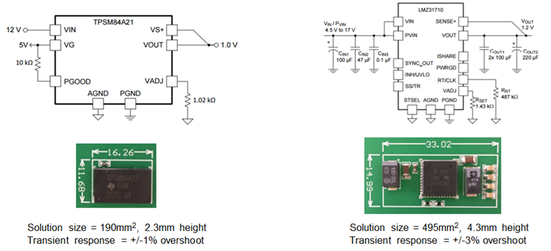
Take for example the TPSM84A21, a 10A DC/DC power module that uses a high-frequency two-phase architecture and switches at 4MHz. The TPSM84A21 integrates 66.1µF of input capacitance and 185µF of output capacitance, a regulator IC, two inductors, and passives in a 9mm-by-15mm-by-2.3mm package. The only external component required is a single programming resistor. For comparison, the LMZ31710 is a 10A DC/DC power module in a 10mm-by-10mm-by-4.3mm package that switches at 500kHz and requires significantly more capacitance than the TPSM84A21, all external to the module. Table 1 compares the capacitance.


TPSM84A21

LMZ31710

Input capacitance

Internal:

66.1µF ceramic

External:

100µF tantalum

47.1µ ceramic

Output capacitance

Internal:

185µF

External:

200µF tantalum

220µF ceramic

Table 1: Capacitance comparison between the TPSM84A21 and LMZ31710

Let’s take a further look at how these two solutions compare in specs, solution size, efficiency, transient response and electromagnetic interference (EMI) performance.

Spec and feature comparison

The TPSM84A21 output range is from 0.55V to 1.2V. The TPSM84A22 is required for output voltages from 1.2V to 2.05V. In comparison as seen in Table 2, the LMZ31710 input range is wider and covers output voltages from 0.6V to 3.6V with a single device.   


TPSM84A21

LMZ31710

Minimum input voltage (V)

8V

4.5V
(2.95V with external bias)

Maximum input voltage (V)

14V

17V

Minimum output voltage (V)

0.55V
1.2V (TPSM84A22)

0.6V

Maximum output voltage (V)

1.35V
2.05V (TPSM84A22)

3.6V

Maximum output current (A)

10A

10A

Typical switching frequency

4MHz

500kHz

Power good

Y

Y

Adjustable soft start

N

Y

Current sharing

N

Y

Adjustable current limit

Y

Y

Frequency synchronous input

Y

Y

Frequency synchronous output

N

Y

Table 2: TPSM84A21 and LMZ31710 spec and feature comparison

Solution size

Figure 1 shows that although the TPSM84A21 package is larger, the overall solution area is 60% smaller.

Figure 1: Solution-size comparison

Efficiency

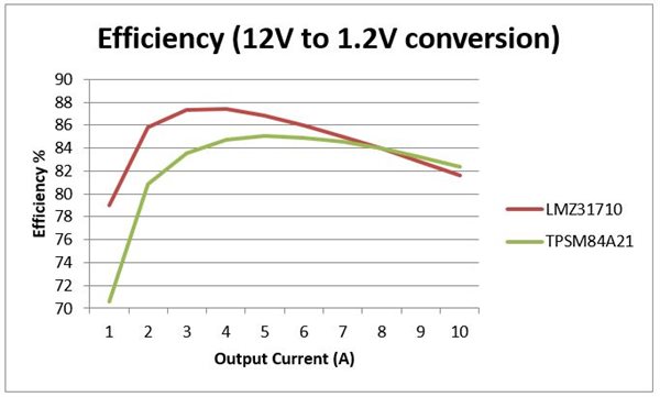
Figure 2 shows that the efficiency of the LMZ31710 is much greater at low to mid loads; however, at full load the efficiency is similar to a 12V-to-1.2V conversion.

Figure 2: Efficiency comparison for a 12V-to-1.2V conversion

Figure 3 shows how the efficiency of the TPSM84A22 and LMZ31710 are similar for a 12V-to-1.8V conversion.

Figure 3: Efficiency comparison for a 12V-to-1.8V conversion

Transient response

As you can see in Figure 4, the TPSM84A21’s transient response is considerably better in a worse-case condition, with no external output capacitance.

Figure 4: Transient response comparison

Radiated EMI

In Figure 5, the radiated EMI of both the TPSM84A22 and LMZ31710 meet Comité International Spécial des Perturbations Radioélectriques (CISPR) 22 Class B radiated EMI, but the LMZ31710 has lower peak emissions.


Figure 5: Radiated EMI comparison

Conclusion

Integrating the input and output capacitors in a small footprint requires a high-switching-frequency architecture, which significantly reduces the overall solution size and transient response and makes the design incredibly simple. The trade-off is a narrower operating input and output voltage range, lower efficiency in some conditions, and higher peak-radiated EMI. With a traditional current-mode buck architecture, the operating range is wider, offering good efficiency and more features. Depending on the situation, both the TPSM84A21/2 and LMZ31710 are excellent options for point-of-load applications.

Additional resources

Use an ULQ buck regulator for energy-efficient power products

$
0
0

Battery life has played a more and more important role in portable devices, contributing to the overall user experience. Longer battery life has become one of the first priorities for engineers to consider when designing a battery-powered device. Energy Star and similar standards not only require increasing the efficiency of a device during normal operation, but also lower energy consumption while in a standby state.

The power-management integrated circuit (IC) implemented in electrical designs is a bottleneck if you’re trying to further conserve energy. Among the various power-management ICs, buck regulators are the most widely used solution. A single electrical design could have several channels of switching buck regulators. These power rails are in either a shutdown or standby state most of the day. The power loss of these power rails under light loads will dominate the overall energy wasted. Most buck regulators on the market use the energy-saving Eco-mode™ pulse-skipping control scheme to increase the light-load efficiency. The Eco-mode control scheme lowers the switching frequency and keeps the high- and low-side power metal-oxide semiconductor field effect transistors (MOSFETs) off for several cycles just after several switching pulses. With less switching loss, the efficiency will increase significantly compared to a non-Eco-mode control scheme device.

Even with the Eco-mode control scheme, it can be challenging to meet energy-efficiency standards. The issue is when the current consumed while both power MOSFETs are off during the Eco-mode control state. The input current in a nonswitching state is called nonswitching quiescent current (Iq), and indicates the minimum current that keeps the internal logic blocks active. With special silicon design, it’s possible to disable most noncritical blocks under a nonswitching state. The always-on blocks, monitor blocks and detection blocks use little current from the IC’s internal power supply. The Iq will stay at the lowest level to save energy. This feature is called ultra-low quiescent current (ULQ). With ULQ, the light-load efficiency will be further boosted during the Eco-mode control state.

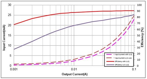
Let’s compare a buck regulator with ULQ (Iq = 45µA) to one without ULQ (Iq = 310µA). Figure 1 is a comparison graph of efficiency and input current under light-load conditions. For a 24V input voltage and a 5V output voltage with no load, the input current for the regulator without ULQ is 0.480mA, while the input current for the regulator with ULQ is only 0.116mA.

Figure 1: ULQ and non-ULQ buck-regulator efficiency and input-current comparison

The ULQ feature is designed to provide extremely low power consumption for battery-powered systems and energy-saving home appliances in their standby modes. Typical battery-powered systems requiring 12V and 24V power rails include portable devices like laptops, cordless mechanical tools with 12V/24V DC motors and wireless speakers. Remote-control systems like drones, car entertainment systems and many other applications also require ULQ to consume minimal current from the battery during standby. Manufacturers of indoor electrical appliances like computers, servers, white goods, heating and cooling systems, home electronics, imaging equipment, and smart home devices are likely to adhere to an energy-efficient standard like Energy Star. The ULQ feature, together with the Eco-mode control scheme, is one big step further for electrical designers attempting to meet energy-efficient standards.

The new TPS54202/TPS54302

To meet energy-saving demands, TI has introduced the TPS54202 and TPS543302. These ULQ buck regulators are 28V, 2A/3A synchronous step-down converters with two integrated N-channel MOSFETs. They implement a fixed 400kHz switching frequency with peak current-mode control. Their 45µA Iq is only 15% of the Iq of devices without ULQ. Figure 2 is a simple TPS54202/TPS54302 schematic.

Figure 2: Simple schematic for the TPS54202/TPS54302


During light-load conditions, the TPS54202/TPS54302 will enter the advanced Eco-mode control scheme state. When the inductor peak current is lower than 300/500mA, the device will prevent high-side FET turn-on and skip pulses for several cycles. During pulse skipping and with both the high- and low-side FETs off, the device only consumes the minimum nonswitching quiescent current from the input source (45µA) by disabling most of the internal circuit blocks. Only some always-on blocks and dynamic bias blocks that keep monitor status and fast recovery remain active. All disabled blocks will wake up once the device exits ULQ mode and the internal FETs start switching again. The ULQ feature ensures that the TPS54202/TPS54302 will have better energy-efficiency performance in standby states.

Using a ULQ buck regulator will bring benefits to the design of energy-efficient power products. For battery-powered devices with ULQ functionality, battery life will be greatly lengthened by reduced standby mode energy consumption. For the home appliances that must pass standards like Energy Star, ULQ technology will significantly improve energy efficiency. The TPS54202/TPS54302 with ULQ will contribute to a better world with low energy consumption.

Additional resources:


Choosing the right charger for industrial batteries

$
0
0


As battery technology enables smaller size and higher capacity, you’ll find battery-powered devices not only in consumer products but also industrial systems. As a designer, one of the most important questions to consider is the control method for the charging system. Should you use a microprocessor-controlled charger or a stand-alone charger?

The two most popular control methodologies are:

  • Inter-Integrated Circuit (I2C)-controlled. The I2C bus is a very popular and powerful bus used for communication between a host device (or multiple host devices) and a single auxiliary device (or multiple auxiliary devices). A microcontroller, known as the host device, is necessary in order to communicate with auxiliary devices, including the charger. It’s possible for the host device to modify tens of charger system parameters via I2C on the fly. Charger status as well as fault conditions can be reported back to the host device.
  • Stand-alone. The charger functions independently without any software or host control. Fixed resistors on the board determine adjustable settings like charge current and voltage limit.

Table 1 lists what you should consider when determining the control method for a charger system.


I2C-controlled

Stand-alone

Need real-time control over the charger?

Ö

X

Need the flexibility of charging parameters?

Ö

X

Need to monitor charging parameter values?

Ö

X

Require a host?

Yes

No

Require software code?

Yes

No

System complexity

Higher

Lower

Table 1: I2C control vs. stand-alone

For industrial systems, the two most popular types of charger designs are:

  • Charging the industrial battery packs inside devices (such as scanners, commercial/police radios and inventory management) via USB. This type of design usually has a built-in microcontroller to support full system functions. An I2C-controlled charger can precisely control the battery charging with the microcontroller.
  • Removing the industrial battery packs from the device and charging them in a cradle with dedicated 9V or 12V adapters. Because the charging cradle is generally simple and cheaper without any microcontroller, you can use a stand-alone charger to charge the battery autonomously.

Figure 1 shows an I2C-controlled charger, where a host (microcontroller) represents the I2C host device and the charger is considered one of the auxiliary devices. The system requires both hardware and software to operate. The host can not only adjust the basic charger voltage and current parameters over wide ranges, but also program safety-timer length, thermal regulation temperature, battery temperature profile settings, boost-mode output voltage and current limit. If any fault occurs, the host will be informed with the fault-condition information. Some advanced chargers may even feed actual charger operating conditions back to the host so that the host can analyze the data and take any necessary action.


Figure 1: Example I2C-controlled charger

Figure 2 shows a typical stand-alone charger. The ICHG pin resistor sets the charge current. The VSET pin voltage controls the charge voltage limit. The ILIM pin resistor determines the input current limit. Once you build the board, there’s no easy and quick way to modify the parameter settings. The STAT pin will blink to indicate fault conditions, but you will have to spend time debugging exactly what is going wrong.

Figure 2: Example stand-alone charger

The control method for a charging system depends on the charging structure and system complexity. Review the overall system carefully to make the right decisions and select successful products.

Additional resources

Getting started with PMBus

$
0
0

I’m working as a product marketing engineer intern, and immediately received several tasks working with many different devices in the TI arsenal. The biggest problem I had was understanding the differences between them. One word that kept coming up (among many) was PMBus – PMBus with telemetry, PMBus without telemetry, etc. Every piece of TI support material highlighted this distinction, but what was it? After answering a few (actually many) questions, my manager asked me to research what PMBus actually was and how to use it, and write a blog post about what I learned for other people in my shoes.

So, what exactly is PMBus?

Power management (PM)Bus is an I2C-based communication standard for power-supply management; in other words, it’s a monitoring and warning system. It’s like when a car starts making a dinging noise because your door is open or you haven’t buckled up. In PMBus, the car is the device, you are the host, and the dinging is the signal PMBus gives so that the host can decide how to respond. In a device, PMBus can monitor input/output (I/O) voltage/current, temperature, fan speed, etc.

The four types of communication between the host and device are command, control, sequence and monitor. The difference between I2C and PMBus is similar to the difference between a sentence and a language, respectively. I2C can write out commands to push through, but it is prone to many errors and is very basic. I2C is preferable if you want to transfer a lot of data, since with PMBus you have to be more specific with commands. This need to be explicit enables more complex commands, along with error prevention.

What benefits does PMBus provide?

Since PMBus can monitor many different parameters in real time, you can program the device to react to certain parameters in a way that will increase efficiency and reliability while decreasing power consumption, which translates to cost savings. The basic form of PMBus has adaptive voltage scaling (AVS) (reduced power usage), multiple rail control (supply sequencing) and power-supply monitoring capabilities. AVS allows you to measure values such as temperature and pressure and use that information for optimizing power, current or voltage. Telemetry is the function of converting the measured information into binary data for optimization and analysis.

How do you set up and use PMBus?

TI has a huge variety of devices that include PMBus and are coming out with new ones every day, like the TPS546C23. For this post, I was able to sit down and use a TPS544C20. To program TI’s PMBus devices, there are Fusion Digital Power™ graphical user interfaces (GUIs) designed to help engineers program and design the chips to their exact specifications. Let’s look at how.

Using the PMBus GUI

Make sure to download the correct GUI. There are three different types designed for different functions: Fusion Digital Power Designer, Fusion Digital Power Studio and Fusion Digital Power Manufacturing.

Fusion Digital Power Designer is the original GUI, and is used for low-voltage and multiphase parts. Designed for engineers trying to configure and monitor devices used in projects, this GUI supports power products, including the UCD9xxx and TPS5xxx families, and is the only tool for configuring devices without having to code.

Fusion Digital Power Studio, a branch off of the original GUI, does the same monitoring and configuring to design devices into projects. The difference is that this GUI supports power products, where coding is necessary. The tool is much simpler than the original, and is a debugging tool. It’s designed for use in conjunction with TI’s Code Composer Studio™ integrated development environment (IDE), or other ARM processor IDEs.

Fusion Digital Power Manufacturing is a simplified version of the GUI and has only three buttons. It is usually used for production, with no built-in debugging features. The GUI programs supported devices to the specified configuration.

For this post, I will be using Fusion Digital Power Designer.

Choosing online or offline modes

Use online when you have a physical device to configure and want to see a real-time response. This is usually when debugging, or in my case, when you just want to mess around with a prototype. If you are using a physical board to program, go ahead and connect it. To start, plug the USB/I/O cord into your device and then into your computer (there will be a small green light-emitting diode [LED] that turns on, indicating that the adapter is connected). From there, attach the ribbon cable to the I/O port of the board, paying attention to the grooves on the connector. Last, plug the power source in. When you open the GUI, it should recognize that a device is connected. 

Use offline when you do not have the actual device, but still want to see what the response will be. This is very useful when designing and getting ahead on projects, or simply evaluating which device is the best fit for your system.

After you open the application, the screen shown in Figure 1 will appear. Chose Offline Mode if you do not have a physical device. If you have a physical device, make sure to connect it and select retry and skip.

Figure 1: Opening Window

Select the first option to start a new project from scratch (Figure 2).

Figure 2: Project Selection

Since you are offline, you need to select the device you want to program (Figure 3).

Figure 3: Device Selection

Make sure to select one of the three options listed in Figure 4 to make the list of devices in those sections appear. Once you’ve selected a device, press OK and Finish.

Figure 4: Device Category Selection

You have now arrived at the home page of the GUI. If you have a physical device and are in online mode, Figure 5 should be your initial landing page. From here, you can configure the device. Click Start Polling to see how the device reacts to the configurations.

Figure 5: Main Page

To navigate, use the tabs in the lower left-hand side of the screen shown in Figure 6. When you have changed something, make sure to Write to Hardwareby using the button in the upper left-hand side of the screen. To save the configuration, use the Store Config to NVMbutton.

Figure 6: Control Window

When I first sat down to look at how to use the PMBus and GUI, I was a little overwhelmed. I hadn’t even opened the package and I was imagining the complicated software I would need to learn to configure the device. After I had a chance to sit down and play with the PMBus and GUI, I realized that it was quite simple to set up and use, almost a plug-and-play type of equipment. What has your experience been using PMBus for the first time?

GaN reliability standards reach milestone

$
0
0

Design engineers faced with the challenges of reduced space and increased power demands are embracing gallium nitride (GaN) technology. By leveraging new topologies, switching frequencies and magnetic design options, GaN has enabled systems to reach unprecedented levels of power density and efficiency. However, these designs need to meet the industry’s expectation for reliability, availability of proven solutions and cost parity with silicon metal-oxide semiconductor field-effect transistors (MOSFETs).

TI has long been a leader and advocate in developing and implementing a comprehensive methodology to ensure long and reliable operation and lifetimes of GaN devices under the harshest operating conditions. To achieve this, the traditional silicon methodology needs to be extended for GaN and its intrinsic characteristics. Additionally, stress testing needs to include the switching conditions of power management, which traditional silicon qualification does not address.

The power electronics industry recently reached an exciting milestone. The Joint Electron Device Engineering Council (JEDEC) announced the formation of a new committee: JC-70 Wide Bandgap Power Electronic Conversion Semiconductors. This committee’s charter is to standardize reliability and qualification procedures, data sheet elements and parameters, and test and characterization methods for GaN as well as silicon carbide (SiC). Having a common standard will enable the power industry to compare and contrast different GaN devices through a single lens. It will also help suppliers better differentiate their solutions and the merits of their technology.

TI is addressing the need for proven and ready-to-use solutions that include:

These solutions, as shown in Figure 1, are not just about 2x the power density. In every stage, GaN-based solutions reduce the number and/or size of both passive and active components (Figure 2), heat sinks, cooling requirements and physical space. These savings help you achieve system-cost parity with silicon MOSFETs with at least 2x the power density.

Figure 1: AC-to-POL solution with GaN


Figure 2: GaN reduces the size of magnetics

As GaN continues on its path forward, we at Texas Instruments are excited to be part of the journey.

Additional resources


LDO Basics: Thermals – How hot is your application?

$
0
0

A low-dropout (LDO) regulator’s nature is to regulate a voltage by turning excess power into heat, making this integrated circuit an ideal solution for low power, or small VIN to VOUT differential applications. With this in mind, choosing the right LDO with the right package is crucial to maximizing an application’s performance. This is where some designers have nightmares, since the smallest available package isn’t always a perfect fit for the desired application.

One of the most important features to consider when selecting an LDO is its thermal resistance (RθJA). This feature illustrates how efficient the LDO is at dissipating heat in a specific package. Higher RθJA values indicate that a package is not very effective at transferring heat, whereas lower values indicate that the device transfers heat more effectively.

RθJA will typically be higher for smaller packages. For example, the TPS732 has different thermal resistance values depending on its package: the small-outline transistor SOT-23 (2.9mm by 1.6mm) package thermal resistance is 205.9°C/W, compared to the SOT-223 (6.5mm by 3.5mm) package’s 53.1°C/W. This means that the TPS732 will experience a rise of 205.9°C or a 53.1°C per 1W dissipated. You can find these values on the device’s datasheet under Thermal Information as shown in Table 1.

Table 1: Thermal Resistance by Package

Do you have the right package?

The recommended operating junction temperature of an LDO is anywhere between -40°C to 125°C; again, you can check these values on their respective datasheets as shown in Table 2.

Table 2: Recommended operating temperatures

What these recommended temperatures mean is that the device will operate as stated in the Electrical Characteristics table of the datasheet. You can use Equation 1 to determine which package will operate at the right temperature:

Equation 1: Junction Temperature Equation

Where TJ is the junction temperature,

TA is the ambient temperature,

RθJA is the thermal resistance (from the data sheet),

PD is the power dissipation and

Iground is the ground current (from the data sheet).

Here is a quick example using the TPS732 to regulate 5.5V down to 3V, supplying 250mA and using both the SOT-23 and the SOT-223 package.

Thermal Shutdown

A device with a junction temperature of 154.72°C not only exceeds the recommended temperature specifications, but it also gets really close to the thermal shutdown temperature. The shutdown temperature is typically at 160°C; this means that if a device’s junction temperature is greater than 160°C then the device’s internal thermal protection circuit is activated. This thermal protection circuit disables the output circuitry allowing the device to cool and protect it from overheating damage. When the device’s junction temperature cools to around 140°C the thermal protection circuit is disabled and re-enables the output circuitry again. If you don’t reduce the ambient temperature and/or the dissipated power, then the device can potentially oscillate on and off as a result of the thermal protection circuit. If you can’t reduce the ambient temperature and/or dissipated power, you’ll have to make design changes to achieve proper performance.

One clear design solution is to use the bigger package, since it operates at the recommended temperature.

Here are some tips and tricks to minimize heat.

Increasing ground, VIN and VOUT contact planes

When power dissipates, heat escapes the LDO through the thermal pad; therefore, increasing the size of the input, output and ground planes in the printed circuit board (PCB) will decrease the thermal resistance. As shown below in Figure 1, the ground plane is usually as large as possible and covers most of the PCB area not occupied by other circuit traces. This sizing guideline is due to the returning current from many components and to ensure that those components are at the same reference potential. Ultimately the contact planes help avoid voltage drops that can hurt the system. A large plane will also help increase heat-sinking ability and minimize the trace resistance. Increasing copper-trace size and improving the thermal interface significantly improves the conduction cooling efficiency.

Figure 1: PCB Layout of SOT-23 Package

When designing a multilayer PCB, it’s usually a good idea to use a separate layer covering the entire board with a ground plane. This helps you ground any component without the need for additional traces. The component leads connect directly through a hole in the board to the layer containing the ground plane.

Mounting a heatsink

Heatsinks decrease RθJA, but add size and cost to the system. When selecting a heatsink, the base plate should be similar in size to the device to which it attaches. This will help evenly distribute heat over the heatsink surface. If the heatsink size is not similar in size to the surface to which it attaches, the thermal resistance will increase.

Due to their physical size, packages like the SC-70 (2mm by 1.25mm) and the SOT-23 (2.9mm by 1.6mm) are not often used with a heatsink. One the other hand, you can pair packages like the TO-220 (10.16mm by 8.7mm) and the TO-263 (10.16mm by 9.85mm) with a heatsink. Figure 2 below shows the difference between the four packages.

Figure 2: Package differences

You can place a resistor in series with the input voltage in order to share some of the dissipated power, an example of this is shown below in Figure 3. The goal of this technique is to use the resistor to drop the input voltage to the lowest input voltage possible.

Figure 3: Resistor in a series configuration

Since the LDO needs to stay in the saturation region to regulate properly, you can obtain the minimum input voltage by adding the desired output voltage plus the voltage dropout. Equation 2 expresses the setting of these two LDO properties:

Equation 2: Maximum Resistance Equation

Using the conditions in the TPS732 example (regulating 5.5V to 3V using 250mA), you can use Equation 3 below to calculate the maximum value of the resistor and the maximum power it can dissipate:

Equation 3: Maximum Power Dissipated Equation

Make sure to select a resistor so as not to exceed its “Dissipating Power Rating”. The rating indicates how many watts the resistor can turn into heat without damaging itself.

So if VIN = 5.5V,

VOUT = 3V,

VDROPOUT = 0.15V (from the datasheet),

IOUT = 250mA and

IGROUND = 0.95mA (from the datasheet), then:

Placement

Other heat-generating devices on the PCB can potentially affect the LDO’s temperature if they are within close proximity to the LDO. To avoid temperature increases, make sure to place the LDO as far as possible from those heat-generating devices.

Conclusion

There are many ways to execute an efficient, size-conscious and low-cost thermal solution for an application. The key lies in early design considerations in order to have all options available. Selecting the proper components is not an easy task when managing thermal considerations, but the right devices and techniques will facilitate a successful design process.

Additional resources:


Upgrade your TO-220 linear regulator with a pin-compatible buck power module

$
0
0

Designers have used linear regulators for decades in electronic applications because of their simplicity and low cost. For a complete step-down power supply, you only need an input and output capacitor along with a linear regulator, which is much simpler to design and has lower noise when compared to a switching regulator. In applications where the input voltage (VIN) is close to the output voltage (VOUT), its efficiency is also high. Because of these advantages, you’ll still find linear regulators used as regulators in low-power systems.

Among the available linear regulators in the market, the UA7805 family is very popular – it comes with fixed output voltages and is typically available in a standard three-pin transistor outline (TO)-220 package (Figure 1). The three pins are VIN, VOUT and GND. A good example is the UA7805, which features a fixed 5V output and benefits from the advantages I listed above. The UA7805 does have an obvious disadvantage in applications where the input voltage is high, however: large power dissipation.

Figure 1: 3-pin TO-220 package 

During operation, the output current is equal to the input current. The internal metal-oxide semiconductor field-effect transistor (MOSFET) mostly works in its saturation region while managing the voltage drop between the input and output voltage. The power loss for the UA7805 is (VIN-VOUT)*IOUT, which for a 12V input voltage and 5V output voltage with only 200mA of output current represents a power loss of 1.4W ( (12V-5V)*0.2A).

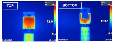
That 1.4W turns into heat, which dissipates through the case and the air. Figure 1 is the case temperature for the UA7805 under 12V to 5V with 200mA output current. Without a heat sink, the case temperature could rise as high as 103.1°C. When taking the thermal resistance from junction to case into account, the internal die temperature is even higher. The TO-220-packaged UA7805 supports output currents of up to 1.5A, but under 12V-to-5V conditions, the UA7805 must significantly limit its output current. With higher input voltages (such as the popular 24V supply), this linear regulator becomes unusable due to thermal issues. Figure 2 is the case temperature for the UA7805.

Figure 2: Case temperature for the UA7805 under 12V to 5V/200mA

For 12V and 24V power bus applications, buck switching regulators are more suitable, as they have better efficiency and thermal performance. The internal power MOSFETs will work in their linear region; only conduction and switching losses will contribute to the device’s power dissipation. Under the same working conditions, the total loss for a buck regulator is much less than for a linear regulator. So if it is possible to upgrade the TO-220-packaged UA7805 with a higher-efficiency buck regulator, you can greatly improve the overall energy efficiency of your system.

There are several challenges if you choose a switching buck regulator to replace the UA7805:

  • More design complexity. Designing a buck regulator requires selecting components such as a filter inductor and capacitors. Tuning control loops also requires a strong power and control background.
  • Higher bill-of-materials (BOM) count. Most buck regulator integrated circuits (ICs) are either controllers or integrated converters. You will need power FETs, an inductor and capacitors.
  • New printed circuit board (PCB) layout design. Most switching buck regulator ICs are surface-mount, and you will need to reroute the PCB layout to replace the UA7805.
  • Possible electromagnetic interference (EMI) issues. A switching regulator can cause noise and EMI issues due to fast switching speeds.

To meet these challenges, TI has released a new buck power module family – the TPSM84203/05/12– developed with the TPS54302 DC/DC converter IC. This family comprises three devices (the TPSM84203, TPSM84205 and TPSM84212) capable of delivering up to 1.5A from a 24V supply (28V max) and providing fixed output voltages of 3.3V, 5V and 12V, respectively.

The regulator IC, inductor, input bypass capacitor and boot capacitor are all integrated into a module. Like the UA7805, there is no need for component selection except for the input and output capacitors. The three-pin (VIN, VOUT, GND) TO-220 package offers pin-to-pin compatibility with the UA7805 and thus provides a significant efficiency improvement without any board change. Figure 3 shows the TO-220 package interior for the TPSM84203/05/12.

Figure 3: Same TO-220 package for the TPSM84205 and UA7805

Figure 3 compares the efficiency and power loss of the TPSM84205 and UA7805. One nice feature of the TPSM84205 is that its light-load-efficiency mode keeps the efficiency high even at low currents, helping minimize power dissipation even when the system is on standby. Figure 4 clearly shows an efficiency improvement for a 12VIN, 5VOUT system of greater than 50% by using the pin-compatible TPSM84205 instead of the UA7805.

Figure 4: Efficiency and power-loss comparison between the TPSM84205 and UA7805

The TPSM84203/05/12 has the same frequency spread-spectrum feature as the TPS54302 to reduce EMI caused by the switching regulator. With the proper external input filter, the TPSM84203/05/12 will easily pass the European standard (EN) 55022 Class B EMI test. Figure 5 is a graph of EN55022 Class B conducted emissions measurements for the TPSM84205.

Figure 5: Conducted emission measurements: VIN = 24V, VOUT = 5V and IOUT = 1.5A

There are many benefits to gain from replacing a UA7805-type regulator with the TPSM84203/05/12 family – the overall efficiency will improve significantly by using a pin-compatible solution with the same BOM count, while the spread-spectrum design ensures that the solution helps meet EMI requirements.

Check out the TI E2E™ Community blog post, “Use an ULQ buck regulator for energy-efficient power products” for the ULQ features of the TPSM84203/05/12 power module family.

Sequencing solutions: simple, reliable and cost-effective

$
0
0

As electronics increase in complexity, designers of even simple systems are running into issues associated with multiple power rails. One challenge with having multiple power rails is often the sequencing of the enable signals, because the startup order and timing of these rails can be strict.

The LM3880 and LM3881 analog power-supply sequencers offer a simple method to control the power-up and power-down sequencing of multiple independent voltage rails. By staggering the startup sequence, it is possible to avoid latch conditions or large in-rush currents that can affect system reliability. The LM3880 has fixed time-delay options for sequencing, while the LM3881 offers variable time delay based on an external capacitor.

One of the most common places you’ll see this need is in a system that includes a field-programmable gate array (FPGA) and/or processors and controllers such as a digital signal processor (DSP) or a microcontroller unit (MCU). Figure 1 shows an example of how you might use the LM3880 or LM3881 in such a system.

 Figure 1: Using the LM3880 or LM3881 for sequencing processors and FPGAs

As you can see, a single LM388x controls up to three voltage rails on its own. You can, however, cascade multiple LM388x devices together in order to sequence additional rails. Each device you add allows you to sequence three additional rails, although if you require sequencing for more than nine rails, it is best to consider a PMBus high-rail-count digital sequencer like the UCD9090A, which can handle 10 rails.

Cascading the LM388x is a very easy task, requiring only two logic gates. The first step is to add an AND gate at the enable signal of the second LM388x with the third rail of the first LM388x as shown in Figure 2. This AND gate ensures the proper power-up sequence by preventing the second LM388x from starting its turn-on until the first LM388x has brought all three of its rails high. The second step is to add an OR gate at the enable of the first LM388x with the first rail of the second LM388x, also shown in Figure 2. This OR gate ensures the proper power-down sequence by preventing the second LM388x from starting its turn-on until the first LM388x has brought all three of its rails low.

Figure 2: Cascading two LM3880 devices

Logic gates can also be useful if you require supervision and monitoring of the rails. You can add three AND gates to the system in-between each rail and between the third rail and a power-on status flag to monitor when all devices are fully powered on. With this simple modification, the power-on status will go active immediately after all three rails power up and will go inactive when the enable turns off, showing that the device is beginning its power-down sequence. Figure 3 shows this application circuit.

 Figure 3: Using AND gates to add supervision

With all of these capabilities, how does the LM388x stack up against other potential solutions? Against more feature-rich (and complex) digital sequencers that provide more functionality (with higher system cost), the LM388x maintains its edge with ease of use, requiring no programming whatsoever, and a very low-cost system approach at nearly tenth the cost of the cheapest digital sequencers. Against a basic discrete solution, the LM388x once again wins when it comes to ease of use, as you can add it to a system as a single device in most cases, allowing not only power-up sequencing but power-down sequencing as well. Compared to other simple analog sequencers, the LM3880 and LM3881 are much simpler; except for a small timing capacitor in the LM3881’s case, they require no external components.

Do you have any sequencing issues? Post a comment below or ask a question on the TI E2E™ Community Sequencers forum.

Signal integrity in multiphase, smart power-stage applications

$
0
0

While a proper high-current power-stage layout is always important in DC/DC applications, paying attention to regulator signal routing during printed circuit board (PCB) layout is more important than ever. Revision 1.3 of the popular PMBus protocol brings with it faster 1MHz clock speeds as well as the option of a high-speed 50MHz AVSBus. These digital lines, along with the quick edged pulse-width modulation (PWM) signals associated with each regulator phase must be properly routed to avoid hampering the ever-increasing analog performance requirements of today’s applications. With the addition of smart power stages into the mix, you also have to factor more analog sense lines into your PCB layout in order to report output current and FET temperature back to the controller. Keeping it all straight can be an engineer’s nightmare.

Figure 1 shows a six-phase buck regulator using the TPS53667 controller and CSD95490Q5MC smart power stage, with the fast edge signals highlighted in red and sensitive analog runs in green. In an ideal scenario, PWM1 to PWM6 and the PMBus lines would be placed on a separate layer from the current, voltage, and temperature sense traces with a shielding ground plane in-between. In space-constrained applications however, such separation is not always possible and one thing you have to watch out for in that case is crosstalk.

Figure 1: Multiphase buck regulator using the TPS53667 and smart power stages

When routing two traces in parallel, some amount of coupling – capacitive, inductive or both – occurs between the two. In digital systems, there should be sufficient noise margin to prevent any sort of corruption, but when a noisy PWM signal is routed next to an analog current-sense trace, as shown in Figure 2, the accuracy of the current-monitoring system is affected.

In the best-case scenario, the controller reports an incorrect current reading to the system. In the worst case, the crosstalk is bad enough to trigger a false overcurrent event and shut the system down. If the VOUT sense lines are routed incorrectly instead, regulation accuracy and loop stability may be negatively affected.

Figure 2: Incorrect routing example

Crosstalk is influenced by a number of parameters, including the spacing between traces, the height above or below a shielding plane, signal rise times, and the length at which the signals are routed in parallel together. For the TPS53667, the controller design sets the PWM edge time while the PMBus specifications set the rise times for the communication lines. Since this is a space-constrained application, we’re assuming we cannot move the PWM and current sense pin (CSP) traces to separate layers. This leaves the spacing of the traces and the thickness of FR4 as the only handles available to minimize crosstalk. See Figure 3.

Figure 3: Microstrip (left) and stripline (right) layout examples

As trace spacing and height are varied, you can draw several key conclusions from Figure 4 in order to combat crosstalk and provide an optimal layout. The goal is to maximize spacing between traces as much as possible, while at the same time making the layer thickness as thin as fab house constraints will allow. Confining the traces to internal layers to create a stripline also cuts down on coupling between traces. Finally, for the best performance and added insurance against unwanted crosstalk, place a ground trace or ground fill between high-speed signals and sense lines for as long as they are in parallel with one another, as shown in Figure 5.

Figure 4: Crosstalk coefficients in decibels for microstrip (left) and stripline (right) layouts


Figure 5: Optimized layout example

With proper planning and a bit of luck, your next converter layout won’t be as constrained as the example shown in this post. Even still, the importance of signal integrity and crosstalk minimization are should be taken into account nonetheless. Always follow the layout guidelines in the data sheet and post your technical support questions in the TI E2E™ Community.


An easy power-module reference design for RF data converter negative voltages

$
0
0

Do you have a need for a negative voltage rail to bias a radio frequency (RF) sampling data converter such as the DAC38RF80? Most applications don’t require the generation of a negative voltage, but you do need it to bias the current sinks in many types of high performance digital-to-analog  converters (DACs). In a multi-channel, multi-device system the total negative supply current requirements can add up; a critical need is to have the right device which can supply these currents in multi-channel systems such as base-stations.

Key system considerations are to meet the total current requirements, low noise, small size and high efficiency; these are requirements for negative-voltage power supplies for data converters which often further challenge system designers to find a power supply that meets their needs in these areas without compromise.

TI Designs are tested and proven reference designs that address such design challenges for specific systems. The 3V to 15.2V Input, 2A, -1.8V Inverting Power Module Reference Design for up to 125°C demonstrates a 2A inverting buck-boost converter. As a bonus, this design uses a simple and highly integrated power module, occupying only 50mm2 of printed circuit board (PCB) area. Figure 1 shows the schematic, while Figure 2 shows the PCB layout.

Figure 1: 2A inverting buck-boost schematic


Figure 2: 2A inverting buck-boost PCB layout

The 2A of output current provided is enough to power as many as four data converters with a single power supply. This provides critical space savings in base stations and test and measurement equipment, where numerous data converters are used in a single system to increase data throughput.

In addition to saving precious PCB space, a power module greatly reduces the required design effort, simplifies external component selection by reducing the number of components, and enables a much simpler and faster PCB layout. The TPS82130 power module used in the reference design switches at 2MHz. This reduces the size of the power inductor, allowing its integration into the power module. This integration means there is one fewer component in the bill of materials (BOM) to select, order and stock as well, as one fewer component occupying PCB space.

A high switching frequency also reduces the output voltage ripple down to nearly unmeasurable levels, as shown in Figure 3. Providing such a low-noise negative voltage allows the data converter to operate at its full performance without distortion. In typical base station applications, you will not need a post-DC/DC linear regulator (LDO) to reduce the noise further.

Figure 3: Output voltage ripple of the inverting power module reference design

Simple, tested, high power, low noise. What else do you need in your negative-voltage power solutions?


Vary the output voltage in an inverting buck-boost topology

$
0
0

In this blog post, I’d like to discuss a methodology for providing a variable output voltage in an inverting buck-boost topology. In this topology, the choice of resistors on the feedback voltage divider network defines the output voltage, as shown in Figure 1.

Figure 1: Configuration of an inverting buck-boost converter

For a different output voltage, you will need to use a different set of resistor values. This may turn out to be a tedious process if the output voltage changes constantly. So let’s discuss a method of current injection that you can use to obtain variable output voltages, without changing the resistor values.

As the name suggests, the current-injection method injects a small current in the feedback divider network to alter the drop occurring across the top feedback resistor, which in turn affects the output voltage. The easiest way to inject current is to use a power supply with a resistor in series, as shown in Figure 2.

Figure 2: Current-injection method using an external supply

If you connect the power supply directly to the feedback divider (without a resistor), the feedback voltage will clamp to a value dictated by the power supply. This is an undesirable situation, because if the clamped voltage is different than the reference voltage of the internal error amplifier, the device will completely turn off, if the clamped voltage is higher than the reference voltage. Or it will remain on continuously, if the clamped voltage is lower than the reference voltage, which can damage the device. In Figure 2, the Rctrl and RFBT are connected in parallel. For that configuration, Equation 1 expresses a linear relationship between the control voltage (Vctrl) and the output voltage (Vout):

The advantage of this method is the ease of implementation; however, it comes with a few disadvantages:

  • Resistor value selection is difficult, as the three resistors need to be accurate in order to obtain the determined value of the output voltage. A disconnection of the external power supply (plugged out) will disturb the feedback network due to the change in resistor values, and you may not achieve the desired output voltage.
  • The feedback node will be at a negative potential and the input of the power supply will be at a positive potential. Also, the positive node of the power supply will be referenced to AC ground. This may cause some instability in the circuit and the design.
  • The configuration will not provide any isolation between the feedback network and the power supply. If the power supply is connected with reverse polarity, it will set Rctrl and RFBB in parallel, in turn affecting the output voltage.

To overcome these disadvantages, consider another configuration, shown in Figure 3, with a slight variation to the first method. This second method uses a p-channel n-channel p-channel (PNP) transistor along with the resistor.

Figure 3: Current-injection method using a level shifter

Equation 2 shows the relationship between the output voltage and the control voltage, which is linear in nature:

In this case, you need to calculate only the values of RFBT and RFBB in order to define the output voltage. The PNP is biased in a manner so that it operates as a constant current source. This variation in the collector voltage (that is, the feedback node) does not affect the injection current.

By using the PNP, the control voltage and feedback node are isolated from each other. Also, the high output resistance of the PNP collector does not cause any instability in the design. If the power supply is connected with reverse polarity, the PNP transistor does not turn on, offering inherent protection. The only downside to this method is that the control of the output voltage is unidirectional and needs an extra component.

Both methods have their own advantages and disadvantages. However, the method using the PNP transistor provides more robustness, along with reliable control and variation of the output voltage.

This technique of varying the output voltage in a buck-boost topology includes the 3.5V to 36V, 5A LM73605 step-down converter. TI offers a wide range of step-down converters, which you can find on the DC/DC switching regulators overview page.

How to approach a power-supply design – part 4

$
0
0

In the previous installments of this series, I focused on specification, transfer ratios and basic power ratings, and buck, boost and buck-boost topologies. In this installment, I’ll introduce the single-ended primary inductance converter (SEPIC) and Zeta converter. Both topologies can be a cost-effective alternative to a buck-boost converter in the power range up to 25W.

SEPICs

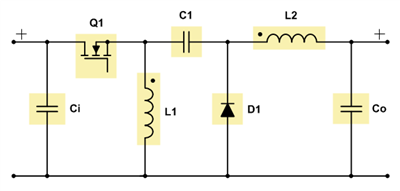
The SEPIC topology can step up and step down its input voltage. The energy transfers from the input to the output when switch Q1 is not conducting. Figure 1 shows the schematic of a nonsynchronous SEPIC.

Figure 1: Schematic of a nonsynchronous SEPIC

Equation 1 calculates the duty cycle in continuous conduction mode (CCM) as:

Equation 2 calculates the maximum metal-oxide semiconductor field-effect transistor (MOSFET) stress as:

Equation 3 gives the maximum diode stress as:

where Vin is the input voltage, Vout is the output voltage, Vf is the diode forward voltage and VC1,ripple is the voltage ripple across the coupling capacitor.

The inductor-capacitor (LC) filter L1/Ci is pointing to the input of the SEPIC. This leads to a smaller ripple at the input due to the continuous current flow. At the output, the ripple is bigger because there’s a pulsed output current.

A nonsynchronous SEPIC costs less than a buck-boost topology because you need only one gate driver (compared to two for a two-switch buck-boost converter) and only two semiconductor components (instead of four). Another advantage of a SEPIC over a buck-boost topology is the better electromagnetic interference (EMI) behavior when both converters are operating in buck mode as a result of the SEPIC’s continuous input current.

You can easily build a SEPIC by using a boost controller because MOSFET Q1 needs to be driven on the low side.

The right half-plane zero (RHPZ) is the limiting factor for a SEPIC’s achievable regulation bandwidth. The maximum bandwidth is roughly one-fifth the RHPZ frequency. Equation 4 calculates an estimation of the single RHPZ frequency of the SEPIC’s transfer function:

Solving Equation 5 for s will have either one or two more RHPZ(s) as a result:

where Vout is the output voltage, D is the duty cycle, Iout is the output current, L1 is the inductance of inductor L1, L2 is the inductance of inductor L2, C1 is the capacitance of coupling capacitor C1 and s is the complex frequency variable.

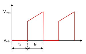
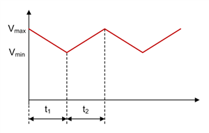
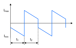
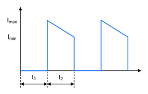
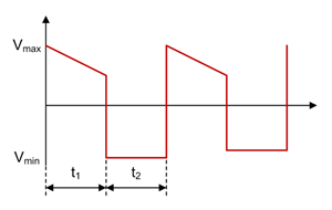
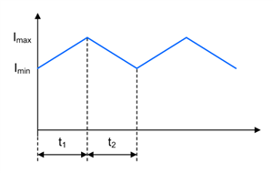
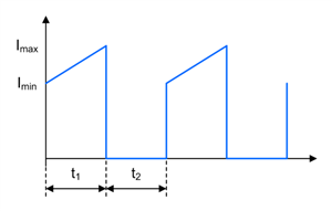
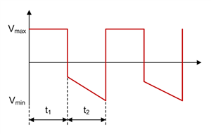
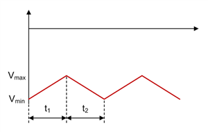
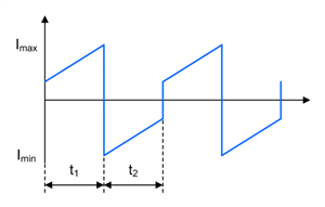
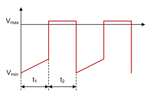
Figures 2 through 11 show voltage and current waveforms in CCM for FET Q1, inductor L1, coupling capacitor C1, diode D1 and inductor L2 in a nonsynchronous SEPIC.

 Figure 2: SEPIC FET Q1 voltage waveform in CCM

 Figure 3: SEPIC FET Q1 current waveform in CCM

 Figure 4: SEPIC inductor L1 voltage waveform in CCM

 Figure 5: SEPIC inductor L1 current waveform in CCM

 Figure 6: SEPIC coupling capacitor C1 voltage waveform in CCM

 Figure 7: SEPIC coupling capacitor C1 current waveform in CCM

 Figure 8: SEPIC diode D1 voltage waveform in CCM

 Figure 9: SEPIC diode D1 current waveform in CCM

 Figure 10: SEPIC inductor L2 voltage waveform in CCM

 Figure 11: SEPIC inductor L2 current waveform in CCM

Zeta converters

The Zeta topology can step up and step down its input voltage. The energy transfers from the input to the output when switch Q1 is conducting. Figure 12 shows the schematic of a nonsynchronous Zeta converter.

Figure 12: Schematic of a nonsynchronous Zeta converter

Equation 6 calculates the duty cycle in CCM as:

Equation 7 calculates the maximum MOSFET stress as:

Equation 8 gives the maximum diode stress as:

where Vin is the input voltage, Vout is the output voltage, Vf is the diode forward voltage and VC1,ripple is the voltage ripple across the coupling capacitor.

The LC filter L2/Co in a Zeta converter is pointing to the output. As a result, the output ripple is smaller compared to the input ripple, because the output current is continuous and the input current is pulsed. I recommend using the Zeta topology for very sensitive loads, where a SEPIC or buck-boost converter would not fit due to their higher output ripple. The Zeta topology has the same advantage regarding cost and component count over the buck-boost converter as the SEPIC.

You can build a Zeta converter by using a buck controller or converter; you will need a P-channel MOSFET or high-side MOSFET driver.

The Zeta converter does not have a RHPZ, as the controller can immediately react to changes at the output. Therefore, you can achieve higher bandwidths with a Zeta converter than with a SEPIC or buck-boost converter while using less output capacitance.

Figures 13 through 22 show voltage and current waveforms in CCM for FET Q1, inductor L1, coupling capacitor C1, diode D1 and inductor L2 in a nonsynchronous Zeta converter.

 Figure 13: Zeta FET Q1 voltage waveform in CCM

 Figure 14: Zeta FET Q1 current waveform in CCM

 Figure 15: Zeta inductor L1 voltage waveform in CCM

 Figure 16: Zeta inductor L1 current waveform in CCM

 Figure 17: Zeta coupling capacitor C1 voltage waveform in CCM

 Figure 18: Zeta coupling capacitor C1 current waveform in CCM

 Figure 19: Zeta diode D1 voltage waveform in CCM

 Figure 20: Zeta diode D1 current waveform in CCM

 Figure 21: Zeta inductor L2 voltage waveform in CCM

 Figure 22: Zeta inductor L2 current waveform in CCM


For both topologies, using coupled inductors instead of two separate inductors has two advantages. The first advantage is that only half the inductance is required for a similar current ripple (compared to a two-inductor solution) because of ripple cancellation by coupling the windings. The second advantage is that you can get rid of the resonance in the transfer function caused by the two inductors and the coupling capacitor. You usually need to dampen this resonance with a resistor-capacitor (RC) network in parallel with coupling capacitor C1.

One drawback to using coupled inductors is that you must use the same inductance value for both inductors. Another limitation is typically their current rating. For applications with high output currents, you might need to use single inductors instead.

You can configure both topologies as a converter with synchronous rectification. But if you do, you need to AC-couple the high-side gate-drive signal, because many controllers require that you connect them to the switch node. Both topologies have two switch nodes each, so take care to avoid negative voltage-rating violations on the switch pin. Two examples with a synchronous SEPIC and a synchronous Zeta converter are the 12V@5A Synchronous SEPIC Converter Reference Design and the 40W Synchronous Zeta Converter with Two Inductors Reference Design, respectively.

Additional resources


Finding the maximum adapter power for the fastest battery charging

$
0
0

Figure 1: Smartphone charging

When you plug in your smartphone to charge, you want it to charge as fast and safely as possible. The integrated circuit (IC) that a smartphone (or other mobile device) cable plugs into is typically a battery-charger IC like the one shown in Figure 2. This IC powers the phone and charges the battery so that it can power the system in the absence of an adapter.

Figure 2: Wall adapter and battery-charger IC

If you’re like me, when you are desperate to charge your phone, you’ll choose any available USB source and/or random cable to charge the battery. If you’re using a lower-power wall adapter (source) or a lower-quality cable, most chargers will reduce the charge current in order to prevent the input source current from exceeding a preset maximum value or the source voltage from dropping below a preset voltage.

These preset voltages and current limits may not be the optimal voltage for the USB source/cable combination, however, and thus the source will not provide the maximum possible output power. It’s no surprise that the more power the source provides to the battery-charger IC, the faster the battery will charge. Ideally, the charger has an algorithm to seek out the source’s maximum power if you’re using an arbitrary, possibly non-USB compliant or third-party adapter and cable combination.

The charger’s preset maximum current varies depending on the type of source. When charging from a legacy USB source, many charger ICs use the USB data lines (D+, D-) to detect the type of USB source (standard downstream port [SDP] or charger downstream port [CDP]) and its corresponding maximum current capability – at least until the USB host is enumerated and can provide more information about the source’s true current capability.

If the IC doesn’t detect a USB source, the source may be a proprietary adapter with its own maximum current capability. Standard “wall-wart” adapters without communication capabilities (dedicated charging port [DCP] adapters) can have a wide range of current capabilities. The charger’s input-current feedback loop (IINDPM) uses the detected current capability to prevent the charger from pulling more input current.

While a legacy desktop/laptop USB port provides only 5V with a known tolerance, newer USB ports and adapters with USB-compatible cables provide even higher voltages with difference tolerances. If the source or adapter cannot provide its rated current, or if you’re using a third-party adapter or a highly resistive (low-cost or extra-long) power cable from the source to the smartphone, then the charger IC’s input voltage and available power drops. In such cases, the charger’s second line of defense against adapter crash and/or oscillation into/out of charging is its input voltage feedback loop (VINDPM), which further reduces the charger’s input current to prevent the input voltage from dropping below a fixed threshold.

Relying on initially detected current settings and present voltage thresholds to obtain maximum power from a power source and cable combination rarely results in the charger extracting optimal power from the source. An input current optimizer (ICO) circuit intelligently identifies and resets the maximum or optimal current (IOPT) that the charger can pull from the power source and cable combination to achieve the fastest possible charge time without collapsing the source.

Figure 3 illustrates the basic operation of the ICO algorithm. The charger pulls increased current until the adapter voltage drops to the VINDPM setting. The charger then takes one input current step back, setting the IINDPM threshold to IOPT.

Figure 3: ICO algorithm illustration

Table 1 shows two different adapters with different current ratings powering a bq25890 through two different USB cables. Cable No. 1 is a high-quality cable with low resistance. Cable No. 2 is a low-cost, extra-long cable with higher resistance.


Table 1: ICO experimental results

Cable No.1 is the recommend, high quality cable. Cable No. 2 is the longer, and therefore more resistive, cable. The ICO circuit detects the real capability of both adapters when powered with cable no. 1. The detected current is slightly higher due to the adapter’s output power tolerance. The current delivery capability is reduced using cable no. 2, but the ICO circuit still detects it. Thus, chargers with ICO provide the best solution on the market to optimize the utilization of adapter power with an arbitrarily selected cable.

When our phones’ batteries are in the red, we all pick the first available adapter source and cable to charge them. A charger with ICO circuitry, like chargers in the bq2589x family, can find the maximum output power capability of most adapter/cable combinations for the fastest battery charging, without adapter overload.

Additional resources

Powering up the performance of sensitive test and measurement systems

$
0
0

When creating high-performance test and measurement equipment, the last thing on your mind is what is powering the board. It may be hard to believe, but the power supply can have a drastic impact on the performance of high-precision successive-approximation-register (SAR) analog-to-digital converters (ADCs) that are downstream to the power supply. Using an electromagnetic interference (EMI)-optimized power supply can be tremendously valuable for a number of different applications, including data-acquisition systems, semiconductor test equipment, spectrum analyzers and oscilloscopes.

By using a DC/DC switching buck converter optimized for EMI performance instead of a standard buck converter, you can achieve an improvement of as much as 2dB and 12dB for the signal-to-noise ratio (SNR) and spurious-free dynamic range (SFDR), respectively. For the analysis, I used two 20-bit SAR ADC (ADS8900B) channels, the THS4551 fully differential amplifier and the LM53635 EMI-optimized 36V buck converter followed by the TPS7A30 low-dropout regulator (LDO); see the Multi-Rail Power Reference Design for Eliminating EMI Effects in High Performance DAQ Systems.

There are three key developments in the LM53635 buck converter that lead to its excellent EMI performance:

  • HotRod™ packaging.
  • Symmetrical pinout enabling concentric current loops for the input capacitors.
  • Spread-spectrum feature.

The LM53635 uses HotRod packaging, which is TI’s implementation of a flip-chip on-lead (FCOL) frame device. Instead of having a bond wire connecting the die to the lead frame, the die is flipped over and directly soldered to the lead frame; see Figures 1 and 2. Removing the bond wire reduces the amount of parasitic inductance, which is a source of high-frequency noise that is difficult to filter out. Another benefit of HotRod packaging technology is that it reduces the drain-source on-resistance (RDS(on)) of the device, which actually improves device efficiency.

Figure 1: Standard wire-bond quad flat no-lead (QFN) device


Figure 2: HotRod FCOL QFN device

Figure 3 shows the immediate benefit of the HotRod package in the switch node of the LM53635 buck converter.

Figure 3: Switch node of standard buck converter with bond wire (a); switch node of the EMI-optimized LM53635 with HotRod packaging (b); symmetrical VIN/ground planes provide an EMI-optimized pinout for the LM53635 (c)

While HotRod packaging improves EMI performance, another optimization is in the pinout of the device. The VIN/ground planes of the LM53635 are designed to be symmetrical, which enables you to place input capacitors in parallel and thus reduce the size of the input current loops. Putting this parasitic inductance in parallel also reduces ringing and helps mitigate high-frequency EMI.

Another great feature of the LM53635 is the spread-spectrum feature, which enhances EMI performance by dithering the frequency ±3% to help reduce the fundamental energy peaks. The spread-spectrum feature can reduce high-frequency peak emissions by up to 6dB and slightly less than 1dB at lower frequencies. With a 36VIN maximum operating voltage, the LM53635 is optimized for systems up to 18VIN and can efficiently convert that voltage down to 3.3VOUT at 2.1MHz. When the voltage exceeds 18V, the device will smoothly fold the frequency back from 2.1MHz.

Another device, the LMS3655, is a 400kHz version of the LM53635 and can efficiently convert a 24VIN down to 1VOUT without any frequency fold-back, since there will be no minimum on-time violations while switching at 400kHz. While the LM53635 offers a smaller solution in inductor and total solution size due to its 2.1MHz frequency, the LMS3655 is optimized for efficiency – with a peak efficiency of 96% with a 12VIN to 5VOUT conversion. Both the LM53635 and LMS3655 share the EMI performance-optimizing features.

Figure 4: High-frequency-conducted EMI results (30-108MHz) without spread spectrum (left) and with spread spectrum (right). The red lines superimposed on the graph denote limits from the stringent Comité International Spécial des Perturbations Radioélectriques (CISPR) 25 Class 5 standard, with 28dB limits from 30-54MHz and 18dB limits from 70-108MHz.

TI tested the LM53635 in the exact same configuration as a similar buck converter not as optimized for EMI with a 24V input, with the output connected to the same LDOs, and tested the performance of the ADCs. Table 1 and Figures 5 and 6 show the impact of the optimizations in the LM53635.

Table 1: The performance of the LM53635 vs. a non-EMI optimized switching buck regulator in the exact same configuration


Figure 5: Spectral analysis of a non-EMI optimized buck converter, showing a number of spurs spiking out


Figure 6: The LM53635 EMI-optimized buck converter with no additional spurs (unlike Figure 5)

You can easily see the performance enhancements of using the LM53635 buck converter for a high-precision application. Using this EMI-optimized device results in a +1dB gain in SNR and a +13dB gain in SFDR vs. a similar buck converter not optimized for EMI. While the power tree is not generally an area that most designers spend a lot of time on, choosing the right switching regulator can have a huge impact on the overall sensitivity of a system.

Additional resources

Power management: the big picture

$
0
0

Figure 1: Remote lake in central Canada

Every few years, my friends and I canoe in the Canadian wilderness for a week, eating only what we can catch (fish) or carry in with us. We cook over a fire and wash dishes with water collected from the lake (trust me, leaving dirty dishes by a campfire is a really bad idea). We are at the mercy of the weather; central Canada in September could be stormy, nearly freezing, too hot or overrun with insects. But it’s a beautiful and unspoiled wilderness, and well worth the considerable effort to get there. You may even spot an animal or two on your journey.

Figure 2: Squirrel in the Canadian wilderness

Being unplugged for several days has its benefits – obviously, just the relaxing aspect of clearing your mind and not multitasking for a while. The focus is on life at a more basic level – daily thoughts include “What am I going to eat?” and “How do I protect myself from the elements?” What always amazes me, though, is the odd feeling of coming back to modern conveniences like air conditioning, running water, electric lights and soft furniture. For all the hassles of modern life, it’s at least more physically comfortable – and probably safer – than what we had before the advent of electrical power.

In elementary school, when we first talked about human civilization, my teacher explained that humans have three basic needs to survive: food, clothing and shelter. Electricity isn’t on that list. But after a few thousand years of recorded history, we seem to have gone well beyond that simple list of three items as far as what people think they “need.”

Most of us are well aware that electrical power – in portable or stationary form – is one of the cornerstones of life. We take it for granted. But now we may have another problem. The human race has been so successful with population growth that we now have to worry about sustainability. The electrical power and technology that helped fuel (no pun intended) our growth will need to be used and generated in ways that minimize their impact on our planet. If not, it could literally be a global disaster.


Figure 3: Solar panels for sustainable energy  

First, we can think about conservation and efficiency. That’s a (relatively) easy first step. Next, we should think about alternative sources for power generation, like the solar panels shown in Figure 3.

These are big problems to solve. But technology, like the power-management devices we develop at TI, will help us get there, step by step. If you are working on any sort of electronic product, how can you make your power-conversion circuitry as efficient as possible? That will help minimize your product’s environmental impact.

Here are some examples to help you learn about improving the efficiency of power-converter circuitry in different applications:

And what about the bigger problem of power generation? Day by day, year by year, technology advances are harnessing the natural forces of solar and wind energy (as well as other possibilities in the long term) that could help us sustain our modern conveniences. These stories from Germany and California are just two examples.


Additional resources


Crank up your power supply with LLC controllers

$
0
0

According to the latest report from the World Bank, energy consumption per capita is increasing exponentially, from 1,200KWh to 3,200KWh. Although there are several driving factors behind this rise in energy consumption, a major one is the increase in the number of electronic devices per household.

Worldwide power consumption increases the need to produce more energy. The question is how to meet this demand for more energy, and the answer lies within the very simple law of economics: supply and demand.

There are two choices:

  • Increase the supply: Electricity manufacturing companies continue to produce more energy.
  • Reduce the demand: Reduce the total power consumption per household which means every power electronics device in household should consume less power.

Figure 1: Supply Demand Curve

While increasing supply seems to be a simple solution, most countries are leaning toward the second option: reducing demand, which would in turn preserve consumption of our natural resources and keep the earth green. Several countries and American states are introducing energy standards like Code of Conduct (CoC) Tier 2, U.S. Department of Energy (DoE) Level VI and California Title 22.

Still, this leads to the next problem: how to control demand when the number of consumers are increasing. The solution to this problem is designing more efficient power supplies that can deliver more energy while wasting less – without creating nightmares for power-supply designers, of course. Designers are looking for magic element that can help them to crank up the performance of the power supply.

TI’s latest inductor-inductor-capacitor (LLC) controller, the UCC256301, introduces a new patented control algorithm, hybrid hysteretic control, to up your game and achieve the industry’s lowest standby power consumption of 40mW with no load. The controller’s ultra-fast transient response enables a reduction of the buck capacitor on the power supply by almost 20%. You can minimize the power loss by rejecting most of the AC ripple, which raises the light load efficiency of the power supply above 90% at a 10% load.

The introduction of this LLC controller comes with a comprehensive tool kit that makes the design experience very easy and leverages several form factor reference designs:

Up your game with LLC resonant controllers

$
0
0

It’s amazing what people will do in order to be the best. For example, athletes will train tirelessly just to shave tenths of seconds off of their race times. Students spend years studying to achieve top honors. Organizations spend decades developing technologies to solve problems that were once only written about in science fiction novels. And finally – nerd alert! – power-supply engineers dedicate themselves to creating converters that are more efficient, with higher density than any converters that came before.

Laugh if you want, but I’ll bet most of you have powered up your circuits and at least achieved personal bests in terms of power density and efficiency that had you outright excited. Maybe you went home and tried to articulate the experience to your spouse or children, only to have them look at you with complete and utter confusion, perplexed at your enthusiasm.

Rest assured, you will receive no such judgment here. Personally, I love the idea of taking something and making it better than it was before. TI has a new controller, the UCC256301, that’s generating a lot of buzz right now because it does exactly that. It takes power supplies that perform well and makes them perform awesome.

The UCC256301 is the newest LLC controller in the TI family, shown in Figure 1. Its features and benefits include integrated high-voltage startup, x-cap discharge, robust fault protection and a new control method that absolutely rocks (more on that later).

Figure 1: UCC256301 system block diagram

In the process of doing competitive analysis, the UCC256301 beats similar devices in stability margin, ease of design, robust protection mechanisms, light load efficiency and transient disturbance rejection.

By way of a practical example (and in keeping with the geeky theme of this post), I took a commercial gaming system and retrofitted it with the UCC256301. Figure 2 shows the before-and-after load transient response.

Figure 2: Transient response improvement

The performance of the original board was actually very good. But dude! Look at what the UCC256301 did to it – the load transient response is now a virtual “don’t care.” To a manufacturer, this could mean up to a 20% reduction in output capacitance, not to mention all of the other component savings from heightened performance and integration. The block diagram in Figure 3 illustrates the different system-level circuits that a device like this saves.

Figure 3: System-level component savings

In this same gaming system, I achieved additional performance enhancements on output ripple voltage during burst mode (10x smaller, Figure 4) and light load efficiency (as much as a 10% improvement, Figure 5). On another system, I even measured less than 40mW of no-load power while fully regulating the output in the presence of a high-voltage power-factor correction (PFC) input. In my mind, this exemplifies the concept of upping your game. I tried to tell my wife and kids about it, but got agonizing blank stares in return.

Figure 5: Ripple improvement


Figure 6: Efficiency improvement

There are many aspects of this device that I could discuss; however, at its heart is a new control architecture called hybrid hysteretic control (HHC). This control architecture combines the best elements of direct frequency-controlled LLC and charge-controlled LLC to come up with something that is better than either. In reality, it is this control method that is responsible for the bulk of the improvements.

So what’s your story? Do you use LLC converters? Do you think this controller is interesting enough that you’d like to learn more about what it can do to up your game? If you have any thoughts on this or anything else, let me know in the comments section below.

(Please visit the site to view this video)

Viewing all 437 articles
Browse latest View live


<script src="https://jsc.adskeeper.com/r/s/rssing.com.1596347.js" async> </script>