Quantcast
Channel: Power management
Viewing all 437 articles
Browse latest View live

More components, more problems

$
0
0

Whenever I watch TV, listen to the radio, or even just look at billboards on the street, I’ll see an advertisement promoting how reliable a product is compared to its competitor. Everyone from car companies to tool companies to semiconductor companies tries to prove that they are the only company whose products you can truly trust and depend on. With so much of a marketing focus on reliability, clearly it’s an important issue. But what does it really mean to be the most reliable out there?

The most basic definition of reliability is the consistency of the measure. If you can consistently produce the same result under the same conditions, then the product is reliable. Simplicity is also an important factor. Reducing the number of parts in a system reduces the risk of one component malfunctioning and negatively impacting performance. For example, in the auto industry, a major concern is the reliability of the internal combustion engine. The functionality of the engine depends on perfectly timed interactions of hundreds of moving parts, so reliability is very important to ensure that cars run properly for 10+ years. Similarly, in the world of power electronics, most DC/DC converters rely on external components to configure the device and achieve the performance that the customer needs. However, every extra external component needed adds additional risk into the system.

Since reliability and simplicity go hand in hand, it is no surprise that the simplest parts to design also tend to be highly reliable. That is because simpler products have reduced bill-of-material (BOM) counts and integrate as many external components into the chip as possible. A high level of integration has several advantages, including reduced BOM count and cost, reduced board space, reduced design work, and higher reliability. The trade-off of high integration is a loss of flexibility. Converters like the TI LM5575 shown in Figure 1 require 12 or more external components to configure features and optimize the DC/DC regulator design to give the best performance for a particular application. Unless the application has particularly stringent requirements, however, the extra work and risk may not be worth it. Would you rather put in the work to complete a complicated design with 14 external components or buy a simpler product with higher reliability?

Figure 1: LM5575 schematic

One way to achieve low BOM count and increase reliability is to integrate the compensation network inside the integrated circuit (IC). Compensation networks are a necessary part of power IC design in order to ensure a stable loop response. Traditionally, power engineers have designed external compensation networks. The advantage of an external compensation network is the flexibility to freely select components and optimize the design to achieve a faster transient response. But designing the compensation is a complex, painstaking process. If you are a power expert with plenty of time, it’s no problem. If you are working under a deadline or do not have the necessary expertise, you may not have the time to properly design an external compensation network. If that’s the case, internal compensation greatly reduces the number of steps and risk in a power IC design. An internal compensation network minimizes the risk of faulty components or a mistake in the design that could negatively affect the end equipment’s performance. It also reduces the time it takes to design the power platform.

Another way TI increases reliability is by offering fixed-output-voltage versions. If you need the flexibility of programming the output voltage, we do have adjustable output options. However, the majority of TI’s customers use buck converters to power 24V, 12V, 5A or 3.3V rails off a battery. Offering fixed-output versions at these voltage levels provides several advantages, including decreasing BOM count, increasing reliability, improving the voltage accuracy of the output, and decreasing output noise. For example, in Figure 2, the LM2596 requires only four external components to function.

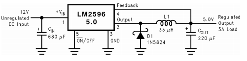
Figure 2: LM2596 schematic

The LM257x, LM259x and LM267x family of products have the lowest BOM count of any SIMPLE SWITCHER® DC/DC buck regulators. By designing our products with simplicity and reliability in mind from the ground up, we are able to reduce the external BOM count needed from 11 components down to four or five components. Every external component that TI can eliminate or integrate inside of the chip has the additional advantage of increasing product reliability while also reducing the amount of design work needed. Make your life easier and choose a buck converter that you can really trust.

Explore our SIMPLE SWITCHER devices to jumpstart your design.  

Additional resources

  • Search for SIMPLE SWITCHER devices that meet your design criteria, and sort the results by low component count.
  • Get more information on the LM2596 and other SIMPLE SWITCHER regulators with low BOM count requirements.


Predicting output-capacitor ripple in a CCM boost PFC circuit

$
0
0

The output capacitor is the main energy storage element in a boost power factor correction (PFC) circuit (Figure 1); it is also one of the larger and more expensive components. Many factors govern its choice: the required capacitance, ambient temperature, expected service life and physical room available. In this post, I want to look at the ripple current that flows in the capacitor. The most accurate way to predict the ripple current is to do a numerical simulation, but there are some simple formulas that can give you a fairly accurate estimate of the currents, as well as some insight into how these currents vary with operating conditions.

Capacitance

As I said, the output capacitor is a relatively expensive component, so you will likely choose the minimum amount of capacitance that still will enable the design to meet its specification. All other things being equal, a smaller capacitor will have a lower cost than a larger one. Two main considerations determine how much capacitance you will need: the required holdup time and the allowable ripple voltage.

For the required holdup time, you can use Equation 1 to calculate the required capacitance:

where Pout is the power taken from the output capacitor, thu is the required holdup time, and Vinitial and Vfinal are the initial and final capacitor voltages, respectively.

If holdup time is not important, then you can size the capacitor according to the allowable voltage ripple. Equation 2 gives Cout as:

where Iout is the load current and Vripple is the peak-to-peak voltage ripple on the capacitor.

Figure 1: Typical boost PFC schematic

Capacitor current

A rearranged Equation 2 can determine the low-frequency ripple voltage on the capacitor. This ripple is sinusoidal, provided that the line current drawn by the PFC stage is sinusoidal. It will be at twice the line frequency and you can calculate the ripple voltage’s peak-to-peak amplitude with Equation 3:

The low-frequency ripple current in the capacitor is very simply related to the output current. Equation 4 gives the RMS (Root Mean Square) value of the current because most capacitors are specified in terms of RMS ripple currents. The result here agrees closely with numerical simulation results:

The ripple current also has a high-frequency component at the PFC switching frequency and its harmonics in addition to the component at twice the line frequency. You can use a slightly modified version of the formula in Erickson and Maksimovic’s “Fundamentals of Power Electronics” to calculate the RMS total capacitor ripple current. This formula ignores the effect of inductor switching-frequency ripple current and thus underestimates the current when compared to a numerical simulation. This underestimation becomes proportionally greater at high line, but because ripple currents are greatest at low line, Equation 5 is accurate to better than about 10%:

The high-frequency component of the capacitor current is then the total current minus the low-frequency current. The result that Equation 6 gives is an RMS value:

Some things to note

I looked at a single-phase CCM (Continuous Conduction Mode) PFC stage in this post, but the low-frequency ripple calculation is also valid for interleaved, CrCM (Critical Conduction Mode) and DCM (Discontinuous Conduction Mode) designs. The high-frequency ripple calculation is valid for single-phase CCM designs only, however.

Both low- and high-frequency ripple currents are not functions of the amount of capacitance. Low-frequency current is a function of the output power; it is not a function of line voltage. High-frequency ripple is greatest at low line and is a function of line, boost inductance and output power.

Check out TI’s portfolio of analog, digital and combination PFC controllers or learn the basics of power factor with the blog post, "What does a beer and power factor have in common?

Quantifying the value of wide VIN

$
0
0

When designing a power supply, one of the challenges designers often face is dealing with voltage transients. It is important to protect circuitry from voltage spikes greater than the rated input voltage (VIN) of the integrated circuit (IC). When dealing with voltage transients, designers have a choice between using a DC/DC converter on the front end of the system with a wide-enough input voltage range to cover any transients, or a lower VIN DC/DC converter with additional clamping circuitry to provide transient protection.

At first glance, it may appear that choosing the first solution, a DC/DC converter with a wide VIN input rating of 36V or 60V, is more expensive because the 1ku price is higher than a converter with a lower voltage input rating. However, the extra voltage-clamp circuitry needed for the transient protection of a lower VIN converter can add 10 to 12 external components that will increase the bill-of-materials (BOM) count and cost, as well as solution size. In this post, I will compare the solution size and cost of the SIMPLE SWITCHER® LM43603 36 VIN, 3A buck converter against a comparable 17 VIN, 3A converter solution with additional clamping circuitry used to absorb the surge voltage. 

The schematic in Figure 1 is an example of a discrete solution used to clamp the input voltage when the IC’s voltage rating is lower than the maximum input spike. This solution uses the LMV431 shunt regulator and a PNP transistor as a control circuit. The P-channel field-effect transistor (PFET) carries the pass-through current and has an increased voltage drop as the VIN surges and thus takes the increased power loss and protects the DC/DC converter. More detail on this technique can be found in the application note “Over Voltage Protection Circuit for Automotive Load Dump.”

As seen in Figure 1, this input clamping control circuitry and PFET adds 13 extra external components to the solution. As Figure 2 shows, based on 1ku quantities published online, these 13 external components would add $1.19 to the total cost. The solution cost of a 17 VIN, 3A converter may be around $1.62, using 1ku-quantity pricing of $0.96 and including the cost of external components like the inductor, capacitors and resistors. This brings the total solution cost of using a 17 VIN buck converter plus clamping circuitry to approximately $1.62 + $1.19 = $2.81. Additionally, the control circuitry and PFET add approximately 210 mm2 to the solution size of the lower VIN solution. A 17 VIN, 3A converter may be around 100 mm2, which makes the total solution size 100 mm2+250 mm2 = 350 mm2.

Figure 2: Control circuit cost breakdown

Another option is to use a DC/DC converter with a wider input-voltage range to cover the maximum VIN spike like the SIMPLE SWITCHER® LM43603 36 VIN, 3A synchronous buck converter. Using a wide-VIN device like the LM43603 enables designers to eliminate the additional clamping circuitry which saves time, cost and board space. The total solution cost of the LM43603 is approximately $2.51 using the published 1ku quantity price of $1.85 and including the cost of external components like the inductor, resistors and capacitors. This means that using the wider VIN LM43063 saves $0.30 or approximately 12%: $2.51 vs. $2.81. The benefits increase when you look at solution size. The total solution size of the LM43603 is approximately 250 mm2 which is about 24% or 60 mm2 smaller than the previous solution.

Another benefit to a wide VIN solution like the LM43603 is increased reliability. As I talked about in more detail in an earlier post, adding additional external components introduces additional risk into the system. The most reliable solution is the simplest solution with the fewest number of external components, because it reduces the risk of one component malfunctioning. Increasing reliability is very important particularly in the harsh conditions of some automotive and industrial applications. Plus, designing the additional clamping control circuitry adds significant work to the design cycle. Using the control circuitry and PFET means that you must select 12 more external components and run additional testing and simulations to ensure that it works. Why put in that effort when you can get a regulator with a wider VIN range with lower system costs and higher reliability?

Of course, pricing and solution size can vary widely based on volumes and contracts between vendors and suppliers, as well as design layouts. The size and cost percentage saved with a wide VIN solution will likewise vary. However, I hope this analysis shows that despite the higher upfront 1ku price, a wide VIN solution like the LM43603 can provide savings in solution cost, board space and design time when dealing with input-voltage transients.

Get more information on TI’s wide VIN DC/DC power solutions.

Designing an IoT modular light

$
0
0

LED lighting applications have revolutionized the world – not only in general lighting but in anything that uses illumination, like LED displays, portable illumination systems, medical instruments and even scientific equipment.

In the winter of 2015, element14, Texas Instruments and Würth Elektronik invited a select group of designers to a “road test plus” – we were told to design something around the TI TPS92512 buck LED driver using evaluation boards and parts. My application was accepted to participate and I went on to implement a simple yet practical Internet of Things (IoT)-based lighting solution that won the challenge in the end.

In this two-part series, I’ll summarize my experience with and thought process behind the challenge, highlighting key milestones in the implementation process. What initially started as a prototype project which could be used for a multitude of things finally evolved into a multipurpose IoT light that I used in my newborn’s room.

The proposal

 My basic idea was to create an IoT lighting-based project, with the ability to connect to the Internet and accept values for color and brightness. The project uses the TPS92512 as the hero of the design, with a TI SimpleLink™ Wi-Fi® CC3200 wireless microcontroller (MCU) LaunchPad™ development kit to enable a Wi-Fi-based connection to the Internet. The commands come in via the Message Queue Telemetry Transport (MQTT) protocol over the Internet, and the TPS92512 controls LED brightness.

 My single-channel LED light prototype is controllable through a website that uses a client-side JavaScript® MQTT library to send commands from a web browser to the TI CC3200 wireless MCU LaunchPad kit via the iot.eclipse.org MQTT broker. I wrote the firmware for the CC3200 device using Energia, which is the Arduino equivalent for TI LaunchPad kits and works even better. Figure 1 shows the initial block diagram.

Figure 1: Proposed system block diagram

Driving LEDs and the TPS92512

Just like any other component, a correctly driven LED will improve its lifespan as well as its efficiency. You can also control the illumination characteristics by varying the drive of the device. The LED is essentially a diode, and the forward-bias characteristics (especially Vf) vary slightly from unit to unit as a consequence of the manufacturing process.

Examining the data sheet for Würth Elektronik’s indium gallium nitride (InGaN)-based ceramic-chip LEDs, you can see that the LED’s forward current increases sharply with the forward voltage and is almost linear beyond the knee voltage. The luminous flux also varies as a function of the forward current up to a limiting value. Thus, it would be more beneficial to control the current through the LED when driving it, using a current-control scheme to obtain better results.

Figure 2 from the mentioned datasheet shows this trend graphically where we see forward current as a function of forward voltage and luminous flux as a function of the forward current.

Figure 2: Forward current as a function of applied voltage and its effect on luminous flux output

There are a number of ways to arrange a constant-current source, including the classic LM317 circuit, as shown in Figure 3. The problem is the maximum current you can drive. You can cascade more than one LM317 in parallel, but that is not very cost-effective.

 Figure 3: Circuit diagram for an LM317 based constant current source

Alternatively, you can use an operational amplifier/comparator with a voltage reference and then use a transistor or MOSFET at the output stage to perform the regulation manually as shown in figure 4. This works better and is how I usually design power-supply circuits. The major issue with this approach, however, is the amount of board space used, as well as bill-of-materials cost. You end up assembling a large circuit – which is OK when you need to handle a lot of current in the range of tens of amps – but for LEDs this is overkill.

 Figure 4: A high side current control circuit using an op-amp

So you need MOSFETs for efficiency but don’t want to make your own module. The solution is a dedicated driver chip like the TPS92512, which has the MOSFET as a switch as well as thermal shutdown, and internal oscillator and pulse-width modulator (PWM) logics for control. Other solutions out there require an external MOSFET switch as well as some miscellaneous passives. The TPS92512 is simpler to use; Figure 5 shows its functional block diagram.

Figure 5: Functional block diagram of the TPS92512

The TPS92512 is capable of driving up to 2.5A; the standard version can operate with a VIN up to 48V. A standard microcontroller with a Pulse Width Modulation (PWM)signal can drive the TPS92512 to vary the output current and therefore LED brightness.

In part 2 of this series, I’ll show you how I built the prototype.

Additional resources

Shrink your industrial footprint with new 60V FemtoFETs

$
0
0

In Shenzhen, China, recently I met with a designer for an infotainment systems manufacturer. “Do you happen to use any 60V load switches in your design?” I asked. He affirmed, telling me he incorporated about 10 30V-60V small-outline transistor (SOT)-23s on his board, generally around 100mΩ RDS(ON). “And on these boards, are you space-constrained?,” I asked. Turns out that he was, so I showed him information on TI’s new CSD18541F5 60V FemtoFET MOSFET, coming in at just under 60mΩ with a 1.5mm-by-0.8mm (1.2mm2) footprint (see Figure 1), that was designed specifically for space-constrained applications such as infotainment systems. 

Figure 1: CSD18541F5 land grid array (LGA) package

That’s roughly one-sixth the size of an SOT-23 (6.75mm2) package for those of you keeping track at home (see Figure 2). It also represents an RDS(ON) multiplied by footprint size figure of merit that is 75% smaller than traditional MOSFETs.

Figure 2: Traditional SOT-23 package next to the CSD18541F5 LGA package

Doing some quick math with this engineer, we determined that with 10 devices per board, he’d be saving roughly 55mm2– not an insignificant amount for a device generally considered an afterthought by most engineers. And what about pad pitch?  Fortunately, the tiny LGA package was designed to accommodate industrial customers as well, for whom the consensus seems to be that a 0.5mm pitch is the preferred minimum distance between pads.

Today, almost everyone I visit in the industrial market, whether they’re manufacturing power supplies, battery protection or power tools, has had some interest in either a smaller- or higher-performing load switch (or both).

So if your industrial design features more than a few SOT-23s or larger load switches, consider switching to our new CSD18541F5 MOSFETs. Trust me, your PCB footprint will thank you later.

Additional resources

Advantages of wide band gap materials in power electronics – part 2

$
0
0

In the first installment of this series, I explored how gallium nitride (GaN) enables operation at higher frequencies and how that allows for smaller component selection. This ultimately shrinks product size while maintaining the same power level: hence the power density increases.

Smaller products: the increasing power density

As the power density of a power supply increases due to the shrinking of its components, what happens to the heat generated?

Heat management can become challenging as the power-loss density increases. For a given aspect ratio, the area available for heat exchange reduces as the volume reduces, which leads to a higher surface temperature.

Efficiency improvements become necessary to enable shrinking in the size of power systems. From a loss point of view, a 90% efficient system has twice as much power loss as a 95% efficient system: every percentage point counts.

Another driving factor pushing for higher efficiencies are the governing regulations and standards for power supplies, which are becoming increasingly stringent. More marketing-related green certifications also require increasingly higher standards.

Improving efficiency

In an application using GaN transistors, you can take two main paths to improve a particular application.

The first is to maintain operational frequency close to an equivalent silicon-based system, since the GaN-based FET has less loss.

The second is to shrink the system by increasing the frequency, in which case transition or switching losses become a dominant element again.

In the second case, where the power density increases, there is a need to further improve efficiency.

The best way to reduce switching losses is to adopt a resonant or quasi-resonant scheme. The same basic concept applies: switch the transistors with either zero current or zero voltage across them (or close to zero). A number of such topologies already exist with silicon solutions that you can extend to GaN.

The advantage of using GaN is that the switching frequencies and transition speeds are high enough that you can use the parasitics from passive components as part of the design to tune the resonance. Smaller parasitics will also result in lower circulating currents and enable shorter dead times. This inherently simplifies the design, reducing cost, weight and all of the extra losses associated with extra components.

You can reduce conduction losses by taking advantage of the high frequency to reduce current ripple (lower current peaks generate lower conduction losses). A good example in AC/DC conversion is an active-switch power factor correction (PFC) circuit, where the charging current is sinusoidal rather than pulsed, thus reducing peak-current conduction losses. Similarly, the effectiveness of active switches can be maximized by using very fast controllers, so to present as low impedance through the power stage, thus improving efficiency.

You can further improve the reduction in driving losses coming from the lowered activation voltage and lower gate charge (Qg) with resonant gate-driving techniques.

Conclusion

Size reduction and improved power-conversion efficiency are the two major visible advantages of using GaN in power systems.

Depending on the system, increasing the frequency beyond a certain limit may not be advantageous for size reduction, as the system’s non-power-related components might not be able to shrink accordingly (power connectors, motors). In those systems, the reason to push for a higher frequency is to push the electromagnetic interference (EMI) beyond the scope of standards.

GaN is the greatest major paradigm shift in power supplies in decades, and with the extremely high switching speeds achieved (100/ns), a GaN switch is the closest thing to an ideal switch available.

GaN opens up the possibility to revisit classic power supplies, improving performance, efficiency, cost and size. More importantly, it enables designers to explore and invent new topologies that were not conceivable with silicon.

Get to know TI GaN solutions and begin your design. 

Power Tips: Shock and Awesome (The PMLK)

$
0
0

A long time ago, in a galaxy seemingly far, far away from my home town, I began my journey as a college student studying electrical engineering in the small city of Gainesville, Florida. Late nights of studying, memorizing theory and endless supplies of coffee powered my battle through electrical engineering. It wasn’t until I started my first lab that things started to make sense.

After six short years later, I work at Texas Instruments (TI) as an applications engineer in power electronics. Upon starting, armed with some power electronics theory from college, I set sail for the laboratory. In my first few weeks, I realized the true power of electronics. While learning, I might have accidentally blown capacitors up, watched tiny flames engulf my MOSFETs and put my (developing) soldering skills to the test, shorting everything the sun touches. I enjoy challenges, so I asked myself, “How could I have been better prepared for this job?”

The answer, just as it was when I started college, was targeted lab work. Since power is a necessary part of every single electronic system (no power = no functioning technology), TI has released a kit aimed at arming students and professionals with the practical power knowledge for both basic power concepts and advanced design requirements. The package is called the TI Power Management Lab Kit (TI-PMLK), and I got the chance to try it out.

Unboxing

The buck kit (there is also an LDO, boost and coming soon, a buck-boost kit) came with a couple of items: a book with six experiments and a circuit board with two buck converter power supplies. The first thing I noticed was the board interface. There are lots of test points, jumpers, and available shunts, which could save lots of time when you want to make quick changes, but don’t want to spend time soldering. 

The book’s preface explains the inspiration, purpose, and structure of the PMLK. The book provided is also available in a PDF format, should multiple people want to use it. The table of contents reveals the lab’s structure. It does a good job of isolating key information with small descriptions to avoid having to go back and forth through pages.  The subsequent pages list the instruments needed, schematics with bills of materials (BoM), and connections for the two bucks. Now it’s time to experiment.

Getting Started

In order to start the first experiment, which focused on the impact of line and load conditions on efficiency, I headed to the lab to get my equipment set up. The book recommends a properly rated DC power supply, oscilloscope, electronic load and multimeters. However, if your lab set up does not come equipped with the equipment listed in the experiments book, there is also a cost effective test methods book which outlines how to perform the measurements using minimal or alternative equipment.

In order to make connections to the input and output terminal blocks, I cut some wire that my connectors could grab on to, and fastened them into the terminal blocks. All of the wire connections between the instruments and your buck converter are listed in the “Experiment Set-Up” page.

After establishing the connections, I read through the first section of the experiment, the “Case Study,” to begin. The case study summarizes the purpose of the experiment and what components we’ll work with. The “Theory Background” section lists useful formulas to compare theoretical calculations to experimental results later in the experiment.  The “Preparation and Procedure” section guides you through a step-by-step on how to power up the board, load the circuit, and measure values. 

Measurements and Calculations

After following the steps, I obtained the switching waveforms on the oscilloscope, along with the voltages and currents at the inputs and outputs. The objective of the experiment was to vary the input voltage and load current to observe their impacts on system efficiency, switching waveforms, and inductor ripple.

Switching and Inductor current ripple waveforms are shown on the oscilloscope while the multimeters from left to right read output current, output voltage, input voltage, and input current

It was awesome to see theory come to life while measuring the switch node and current ripple, as it confirmed calculations and graphs seen in the classroom. After taking the measurements, the next step is to compare experimental results to the theoretical results. Armed with equations from the theory section and a TI-89 graphing calculator, I began calculating.

After completing the calculations, you are prompted with a few questions that are answered in the “Discussion” section later in the experiment. The experiment also provides some plots to that I could compare to mine, and does an excellent job of explaining the phenomena that I saw.

Overall, the TI-PMLK is an excellent tool for any student or professional. The experiments in the book cover many topics and challenges we see in industry today and relates that to the power supply performance trade-offs an engineer has to make to design it into a system. The kit stimulates interest with hands-on experiments and brings paper theory to life with practical engineering experience.

As a recent college graduate, I like that the TI-PMLK arms new engineers with the basic experience and tools you need when venturing into the world of power electronics. If you are a seasoned engineer, the TI-PMLK can also provide you with training to help make meaningful design decisions that improve size, cost and efficiency. Overall, I highly recommend the TI-PMLK and can’t wait to also test out the LDO and boost boards.

Learn more about the TI-PMLK.


A smaller step-down power module for communications equipment systems

$
0
0


The proliferation of cellular phones, tablets and other Internet-connected devices (the Internet of Things) has drastically increased the amount of wireless communications traffic throughout the world. This requires a corresponding capacity increase in the communications infrastructure– such as base stations, remote radio units (RRUs) and small cells (femtocells) – to handle the increased throughput. While commuting home today, take a look at how many base stations and antennas you can see on the tops and sides of various office buildings, water towers, sports stadiums and other structures. There are so many and they are everywhere!

As a consequence of the sheer number of base stations, a key design challenge is size. As the power supplies inside the base stations become smaller, you can add more data channels to increase throughput. But with more channels occupying the same space, heat generation and the corresponding temperature rise inside the base station become problematic. A step-down DC/DC converter creates less heat than a linear regulator (LDO) and thus a lower temperature rise inside the base station; this is even more critical as the overall system channel and power density increase.

Figure 1 shows the efficiency of a typical step-down DC/DC power module used in base stations. A linear regulator at the same 12V input voltage and 5V output voltage achieves a maximum of 42% efficiency.

Figure 1: The TPS82130 power module’s efficiency with a 5V output

A power module with numerous integrated components is an obvious choice to achieve a smaller total size. But finding one that can operate from the typical 12V input voltage and deliver output currents above 1A is challenging. The TPS62130 is a nonmodule or discrete IC power supply that supports up to a 17V input and 3A output currents. While it contains internal transistors and control-loop compensation to enable small size, it requires at least seven external components for a complete solution that occupies about 100 mm2.

The TPS82130 is a MicroSiP power module based on the TPS62130. It integrates the power inductor – typically the largest component in the power supply – and reduces the external components to just five. The total solution size is cut by more than half, to about 42mm2.

Figure 2 shows a complete TPS82130 solution’s printed circuit board (PCB) layout. As an added benefit of being a module, the PCB layout is greatly simplified compared to the discrete TPS62130.

Figure 2: The TPS82130 power module requires just five external components

To support a wide variety of application conditions, the feature set with both devices is nearly the same: enable and power-good pins for sequencing, a soft start and tracking pin for controlling the output-voltage rise time, high efficiency for a low temperature rise, and stability with a variety of output filters due to the DCS-Control topology. Both devices operate from common 5V or 12V rails or any voltage between 3V and 17V. Both the feature set and input-voltage range provide a flexible solution suitable for different power architectures or specific application requirements.

How can a power module shrink your power supply’s size?

Additional resources


Designing an IoT modular light – part 2

$
0
0

In the first installment of this two-part series, I talked about an illuminating idea I had for a project I could use in my newborn baby’s room: an Internet of Things (IoT) modular light. I’ve done the prep, so now let’s create the prototype.

Creating a prototype

As shown in the block diagram in Figure 1 from the previous post, a TI SimpleLink™ Wi-Fi® CC3200 wireless microcontroller (MCU) LaunchPad™ development kit connected to the TPS92512 drives a light-emitting diode (LED) array. I used a 12V switch-mode power supply as the power source and wrote the firmware for the CC3200 using Energia. You could also write the firmware using Code Composer Studio™ integrated development environment (IDE) software, which is my favorite tool, but in this case, the example code and Arduino-like interface accelerated the prototyping stage immensely.

I set up the CC3200 wireless MCU LaunchPad kit with the latest firmware and programmed the kit to talk to a particular topic at the Message Queue Telemetry Transport (MQTT) broker. MQTT is a protocol with very small overhead and allows for a server/client topology to create communication connections over the Internet. Facebook Messenger uses MQTT, and it is one of the more popular protocol projects being tuned to power the future IoT.

For my project, I also designed a small printed circuit board (PCB) that I framed as a Booster Pack™ plug-in module; the result is shown in Figure 1. You can stack a number of these PCBs to achieve the required number of LED drive channels.

Figure 1: A screenshot of the schematic for the TPS92512 BoosterPack

I was able to fit the design into a 50mm-by-50mm form factor, which would reduce manufacturing costs if mass-produced. Figure 2 shows a screenshot of the final layout which has four mounting holes as well as the BoosterPack module pin conformity.

Figure 2: Screenshot of the final layout for the TPS92512 BoosterPack

I used the schematic and layout from the evaluation module as a guide.

Würth Elektronik provided the coils as well as the electromechanical parts, which was a big help since they made the footprints for all of the parts available as well. Getting the board design ready was a breeze. Printing the layout and checking the footprints as shown in Figure 3, confirmed that everything was indeed in order.

Figure 3: Footprint verification via 1:1 paper print of the layout

The Web client design

With my basic understanding of HTML, Code Composer Studio IDE and JavaScript®, I was able to create a simple user interface (UI) for my project. The idea was to create buttons in a web interface and then use JavaScript to send the commands via MQTT to the broker and finally to the IoT light. I used the Paho library in JavaScript and performed a bit of cosmetic surgery via Code Composer Studio to create a webpage that looks nice; Figure 4 is a screenshot.

Figure 4: The live webpage for remote control

I kind of went overboard with the home-automation front end, but you get the idea. I wanted a look-and-feel I would be willing to pay money for. In the end, four buttons was all I needed and they worked out pretty well. The page uses Twitter Bootstrap, which means the same webpage will look different on different screen sizes.

The love and romance

I had worked out the technical details of the project, but it was more or less a science project. The real evolution came when my wife suggested that I turn the prototype into a real product for our own use. We were expecting a baby at the time and she requested a room light whose brightness we could control remotely. The same light would be usable as a room light, a night-light and a midnight-diaper-change light. Instead of 3-D printing an enclosure or something, I decided to recycle an old LCD monitor, some glass and a birthday card from before we were married. The romance was still alive and it was time to light things up. The manual layout of the components inside the enclosure is shown in Figure 5.

Figure 5: Various modules laid out in the recycled PC monitor

Putting humpty dumpty together was fun and the finished product is shown in Figure 6.

Figure 6: The final product

The final product is not particularly a product so much as a piece of technology fused with a personalized artifact. Our baby currently enjoys staring at the final outcome above his crib and we are thankful for it.

Future work

I am currently working on creating a grow light for indoor hydroponic farming based on the same concept, which thus represents an additional application.

Security was never important for this demo but is crucial for IoT products, so I am working to implement a more secure solution. I am experimenting with Raspberry Pi as a local broker, as well as considering porting the entire web UI to the SimpleLink Wi-Fi CC3200 device itself. Both solutions are viable but cannot be an IoT solution, since they will no longer require an Internet connection nor be accessible over the Internet.

Conclusion

This project is a proof of concept but with a personal touch. I have had a lot of requests from friends to make one for them. So far I have declined, but maybe in the future I can provide a Phillips Hues alternative.

The important thing about this project is it proves it is quite easy to come up with an IoT prototype quickly and easily with the amount of resources available. Thanks to Texas Instruments, Würth Elektronik and element14 for their support. The future is indeed bright.

Additional resources

FemtoFET MOSFETs: small as sand but it’s all about that pitch

$
0
0


What contains more silicon: a grain of sand or TI’s latest FemtoFET product? As I sit in my beach chair watching the waves of the Atlantic roll onto the Jersey shore, my mind drifts over this question. The newly released F3 FemtoFETs, boasting a miniscule body size of 0.6mm by 0.7mm by 0.35mm (see Figure 1), can easily rival the grains of sand blowing under the Atlantic City boardwalk.

Figure 1. F3 FemtoFET package size.

Check out the latest products to join the FemtoFET portfolio in the table below, including the ultra-low capacitance CSD15380F3.

Part Number

N/P

Vds

Vgs

Id Cont. (A)

Typical Rdson (mohm)

Ciss (pF)

4.5V

2.5V

1.8V

CSD15380F3

N

20

10

0.5

1170

2200

x

8.1

CSD25480F3

P

20

12

1.7

132

203

420

119

CSD23280F3

P

12

6

1.8

97

129

180

180

Table 1. F3 FemtoFETs

With devices this small, a critical consideration is the surface-mount technology (SMT) equipment used to attach the FemtoFETs to the board. The pitch of the device pads is the determining factor as to whether a customer’s SMT equipment can handle a package. Most high-volume personal electronics manufacturers have SMT equipment that can handle a minimum tolerance of 0.35mm pad pitch, but the SMT equipment at some industrial customers can only go down to a 0.50mm pad pitch.

The FemtoFET’s land grid array (LGA) package is similar to a silicon chip-scale package (CSP), except that the LGA has no attached solder balls. The gold-plated leads on the F3 FemtoFETs maintain the same 0.35mm pad pitch used on TI’s previous-generation F4 FemtoFETs. This enables existing F4 customers to use the smaller devices with full confidence that their SMT equipment can handle them.

In order to extend FemtoFETs into industrial applications, TI is also introducing a line of F5 FemtoFETs with a 0.50mm pitch, expanding the voltage range up to 60V. To learn more about this 60V F5 device, see my colleague Brett Barr’s blog post, “Shrink your industrial footprint with new 60V FemtoFET MOSFET.”

TI recommends Pb-free (SnAgCu) SAC alloy solder paste when board-mounting FemtoFETs such as the SAC305. You can use Type 3 paste, but the smaller-diameter Type 4 solder paste is preferable. The paste should be no-clean and water-soluble, although flux cleaning after board mount is still a good idea.

A stencil defines the locations where you should deposit the solder paste on the board. The thickness of the stencil and the x-y dimensions of the openings are important parameters. The maximum stencil thickness should be 100µm.

A wide variety of wearables and personal communication devices use low-leakage FemtoFETs. With gate and drain leakages typically in the single digit nano-amp range, FemtoFETs help to ensure that the battery charge of your personal electronics device lasts for the full day at the beach. With over 500 million FemtoFETs shipped since their introduction in 2013, as I relax on Long Beach Island this summer, I will be dreaming of all those pitch-perfect grains of sand. Get more information on TI’s family of FemtoFET MOSFETS.

Additional resources


Powering the Altera Arria 10 GX

$
0
0

Field programmable gate arrays (FPGAs) are increasingly complex system on chips (SoCs) that include not just programmable logic gates and random access memory (RAM) but also analog-to-digital converters (ADCs); digital-to-analog converters (DACs); and programmable analog features and signal-conditioning circuits that enable high-performance digital computations in servers, network-attached storage (NAS), enterprise switches, oscilloscopes, network analyzers, test equipment and software-defined radios.

Altera’s Arria 10 SoC is such an FPGA. One of the Arria 10’s power-reduction techniques is smart voltage ID (SmartVID), which offers a large number of very small-voltage reduction steps that are programmable into the FPGA’s nonvolatile registers in order to reduce the power dissipation of the chip.

The FPGA is smart enough to monitor its own temperature and tell the external Vcore voltage regulator what Vcore value to output to the FPGA in order to minimize its power consumption and increase efficiency. Because the registers use nonvolatile memory (NVM), the new programmed Vcore value becomes the default value after recycling the FPGA power.

Arria 10 SmartVID FPGAs power up at a nominal Vcore voltage of 0.9V; after that, the Vcore value is adjustable down to 0.83V in discrete, small steps.

One of the SmartVID communication interface options between the Arria 10 FPGA and the external Vcore voltage regulator is the PMBus digital serial interface at a 400kHz clock speed. In a PMBus system, the Arria 10 FPGA acts as a PMBus master or a slave – whatever you prefer.

If the Arria 10 is the PMBus master, it will communicate via PMBus to the Vcore voltage regulator (acting as the PMBus slave) the new Vcore value in a range between 0.83V and 0.9V using the standard PMBus command “VOUT_COMMAND” – 21h code. The PMBus master uses the VOUT_COMMAND instruction in the data format retrieved from VOUT_MODE to write voltage ID values to the regulator. The PMBus Vcore regulator will then set its output voltage to the new commanded value as dictated by the FPGA. The voltage ID voltage can change by no more than 10mV per step.

The regulator(s) must meet the static, ripple and dynamic power tolerances listed in the “Arria 10 GX, GT, and SX Device Family Pin Connection Guidelines” during all phases of power delivery after the boot voltage is reached.

To implement SmartVID with PMBus, you must enable PMBus in the FPGA with Quartus Prime software version 15.1. Only the Arria 10 VCC and VCCP rails can use SmartVID; there is an option to combine VCC/VCCP with VCCERAM rail, but then SmartVID implementation is not possible.

The power tree in Figure 1 corresponds to the Arria 10 GX FPGA, which is the highest-performance Arria 10 member in the SoC family, and shows TI SmartVID solutions for the Arria 10 FPGA core rail through PMBus.

Figure 1 – Altera Arria 10 GX power solution with SmartVID PMBus implementation for VCC/VCCP

The TPS53647 is a PMBus four-phase driverless pulse-width modulation (PWM) controller, with extensive pinstrapping and PMBus programming, configuration, control and monitoring of input/output voltage, current, temperature and power. The TPS53647 is paired with TI’s CSD95372B power stages, which include high-performance NexFET™ gate drivers and high- and low-side NexFET power MOSFETs stacked on top of each other in a PowerStack™ packaging configuration for high efficiency, optimal thermal performance, easy heat sinking and high power density.

So if you are designing with Altera’s Arria 10 FPGAs and looking to implement SmartVID via PMBus, consider TI’s PMBus DC/DC solutions for the VCC and VCCP rails.

Additional resources

Enabling 48V-to-POL single-stage conversion with GaN

$
0
0

Enterprise server, switch, base station and storage hardware designers are always looking to increase power density and efficiency on their motherboards. With the addition of more components on the motherboard and a shrinking form factor, power-supply density becomes the limiting factor in reducing the area further. The smaller the power supply, the smaller the motherboard and reducing motherboard size enables fitting more boards into a given rack to maximize data-center throughput and performance.

In the typical telecom power-supply system shown in Figure 1, the 48VDC input voltage has to be further stepped down to an intermediate bus voltage (3.3V in this case) which one or more buck direct current (DC/DC) converters then take and step down to various regulated lower-output voltages needed for processor, ASIC, and FPGA core rail voltages, I/O rails, DDR memory, PHY chips and other low-voltage components.

Figure 1: An alternating current (AC) to 48V to point-of-load (POL) telecom power system

TI’s gallium nitride (GaN) DC/DC solutions eliminate the intermediate bus DC/DC conversion stage so that designers can step 48V down to lower output voltages in a single stage.

Eliminating the intermediate bus DC/DC converter enables significant increases in power density and system cost, with an accompanying increase in reliability.

GaN’s advantages over silicon MOSFETs include:

  • Low input and output capacitance to reduce switching losses and enable faster switching frequencies.
  • Near-zero reverse-recovery charge for no reverse-recovery losses and reduced losses in Class-D inverters/amplifiers.
  • Greatly reduced switching losses due to lower gate-drain capacitance, enabling higher switching frequencies and reducing or even eliminating heat sinks.

Figure 2 shows a 48V-to-POL efficiency comparison between GaN and silicon FETs.

Figure 2: 48V-to-POL GaN vs. silicon DC/DC converter efficiency with varying load current

TI’s new 48V-to-POL GaN single-stage solution– using the TPS53632G driverless pulse-width modulation (PWM) controller and LMG5200 80V GaN half-bridge power stage (drivers and GaN FETs in one integrated circuit) – enables high power density, fast load-transient response, high efficiency, excellent thermal performance and increased system reliability in a total area of ~700mm2 for 48W of output power. Efficiency is ~88% at 48V with 60V input, 1V output, 50A and a 600kHz switching frequency, as shown in Figure 3.

Module efficiency peaks at ~91% and is still ~90% at 35A of output current. Notably, efficiency does not significantly drop even when increasing the input voltage to 75V.

Figure 3: 48V-to-POL GaN DC/DC converter reference design and efficiency with varying load current at 600KHz

If you are designing 48V-to-POL DC/DC converters for end applications such as enterprise servers, switches, base stations and storage and have traditionally used 48V-to-intermediate bus and intermediate bus-to-POL DC/DC converters, it’s time to simplify your design and increase power density and reliability with TI’s GaN DC/DC solutions. Check out TI’s complete GaN DC/DC conversion portfolio on the GaN Solutions portal.

Scope plot surgery – my boost converter has an off-ramp!

$
0
0


As an applications engineer, I often get inquiries about voltage and current flows in switching regulators. And I often realize that the basic theory I learned in college doesn’t always tell the whole story. A recent case with the asynchronous boost converter in the TPS65150 LCD bias device is a good example of what I mean.

Let’s start with the basic theory of how the switching node of a boost converter should look. Figure 1 shows the basic structure of an asynchronous boost converter.

Figure 1: Simplified boost converter block diagram

When transistor Q1 turns on, the switch node pulls to ground and inductor L1 charges. The voltage on the switch node is approximately equal to 0V during the on time. During the off time, Q1 turns off, L1 discharges to the output, and the voltage on the switch node equals the output voltage (VO) plus the forward voltage (VF) across diode D1.

Figure 2 shows the switch-node waveform under typical operating conditions. As expected, the voltage on the switch node is rectangular and alternates between ground and VO + VF.

Figure 2: Switch-node waveform

But under low-output current conditions, the switch-node waveform shape changes and looks like Figure 3. At the start of the off time the switch-node voltage is VO + VF (as before), but then it ramps down linearly. What’s causing this behavior and what’s the difference to the basic theory?

Figure 3: Switch-node waveform at low-output currents

The internal block diagram shown in Figure 4 reveals the reason for the sloping waveform: an additional PMOS transistor (Q2) connected across the diode rectifier. This transistor is a synchronous rectifier that lets the converter operate in continuous conduction mode (CCM) under all operating conditions. It is on when the inductor current is negative and off at all other times. Because it is not the main rectifier, the Rds(on) of Q2 can be relatively high (a few ohms) without decreasing efficiency much, but the high Rds(on) causes a voltage drop on the switch node when the negative inductor current flows through it. And because the inductor current is linearly increasing, the voltage drop also increases, causing the slope shown in Figure 3.

Figure 4: Internal block diagram showing synchronous rectifier

Figure 5 shows the inductor current as well as the switch-node voltage and confirms that the ramp on the switch-node voltage starts when the inductor current goes negative, and increases as the inductor current increases.

Figure 5: Switch-node voltage and inductor-current waveforms

Be aware that the ramp starts for all output currents below the critical conduction point. You can calculate the critical conduction current with Equation 1:


where D is the duty cycle (boost:   
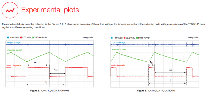
), L is the inductance and  is the switching frequency.

If you want get a deeper understanding of voltage and current flows in switching regulators, download the tool, “Power Stage Designer of Most Commonly Used Switch-Mode Power Supplies.

If you have experienced similar waveforms in your power-supply design of power supplies that you cannot explain – but would like to know the reason for, – just add a comment below.

Additional resources:

Powering Intel’s Xeon D SoC in servers, storage and switches

$
0
0

Intel’s Xeon D chip, developed under the Broadwell-DE code name, is the first Xeon central processing unit (CPU) to bear the system-on-chip (SoC) title by including two physical chips in one package. This 14nm SoC has the cores, memory controllers, L3 cache, dual Ethernet and Peripheral Component Interconnect (PCI) Express 3.0 controllers all on one die.

A second chip – what used to be called Southbridge – includes legacy PCI Express 2.0 peripheral slots and USB/Serial AT Attachment (SATA) ports, and connects to the first chip in the same package through a dedicated link.

The Xeon D SoC makes it possible to develop high-density servers for hyperscale workloads and fits well within cloud infrastructures where servers, storage and networking switches interconnect.

TI’s complete power solution for Intel’s Xeon D SoCs includes the TPS53631 and TPS53641 VR12.5 driverless 3- and 4-phase pulse-width modulation (PWM) Vcore controllers with the Power Management Bus (PMBus).

You can evaluate the 45W and 65W Xeon D CPU, double-data-rate (DDR) memory core and chipset core multiphase power-supply performance with the TPS53631/TPS53641 evaluation module, shown in Figure 1.

The Vcore controllers are on the east side of the socket, while the power stages and output inductors are on the north side.

The evaluation board has the Intel CPU interposer and socket in order to accept Intel’s voltage transient test tool (CPU emulator) for testing. It also has a PMBus connector to configure, control and program the controllers via PMBus, as well as to monitor the input and output voltage, current, power, temperature and report-fault conditions through TI’s Fusion Digital Power Designer.

Figure 1: Xeon D System V Interface Definition (SVID) Vcore power-supply evaluation module

TI has a complete Xeon D TI Designs reference design for the three Intel SVID rails: CPU, DDR core and chipset core. The reference design features:

  • Complete three-rail VR12.5 SVID power solution for Intel Xeon D platforms.
  • PMBus programming of VID, SoC load line and voltage margining.
  • PMBus monitoring of input/output voltage, current, power and temperature.
  • Complete test report per Intel test template guidelines – see the load line (output voltage vs. load regulation) example shown in Figure 2.

Figure 2: Xeon D SVID Vcore power-supply load line as tested on the TPS53631/41 evaluation module

If you are designing with Intel’s Xeon D processors (D-1548, D-1557, D-1567, D-1571 and D-1577), TI has power solution and reference design support tools to enable your high-performance microserver, enterprise switch or storage system. To receive the complete Xeon D TI Designs reference design for the three Intel SVID rails, email vr@list.ti.com.

Can an LDO produce better-quality images in small-sized camera applications?

$
0
0

Digital imaging electronics are becoming more portable and integrated into high-quality solutions. The cohesiveness of high-performance and small-sizes in camera applications is often influenced by the low-dropout (LDO) voltage regulators powering the complementary metal-oxide semiconductor (CMOS) image sensor in cameras. Figure 1 is an example of the circuitry used for cameras in a smartphone. 

Figure 1: Camera circuitry in a smartphone

We’ve all heard the term “pixel,” but what does that mean to consumers? Pixel size can help determine the size of each discrete photodetector in a CMOS image sensor. It is imperative to know the size of these photodetectors because that is what captures light to record the perfect image. Figure 2 illustrates the process.

Figure 2: Production of high-quality images

So all you need is a large image sensor to capture good quality images, right? Not quite. These CMOS image sensors need to be powered in a specific way given their sensitivity to noise. The components that make up a CMOS image sensor are extremely susceptible to transients caused by the power supply. A noisy power supply affects a pixel’s ability to properly capture light, which results in a poor-quality image. Figure 3 is an example of a high-level power-tree block diagram for powering a CMOS image sensor.

Figure 3: High-level power-tree block diagram for a CMOS image sensor

An LDO voltage regulator filters out the unwanted noise from the power supply. To power the image sensor, you will want to look at the noise specs of the LDO to make sure it meets the specifications of the end equipment. Let’s use the LP5907, a high-performance LDO, as an example.

Figure 4 shows the power-supply rejection ratio (PSRR) swept from frequencies between 10Hz to 10MHz. The PSRR characterization allows the LDO to block noise produced by the power supply. Simply put, the higher the PSRR, the more noise the LDO can block from the power supply.

Figure 4: LP5907 PSRR

But this is only at the input of the LDO; what about the output? That is where spectral-noise density comes in. Figure 5 shows the output-voltage noise swept between 10Hz to 10MHz. The lower the output-voltage noise, the less noise transferred into the CMOS image sensor.

 Figure 5: LP5907 spectral noise density

Table 1 lists the LP5907’s PSRR and output-voltage noise specifications. 

Table 1: LP5907 PSRR and output-voltage noise

The LP5907 has an extremely high PSRR of 82dB at 1kHz and 6.5µVRMS at a full load current. The combination of these parameters suggests that this LDO could be an essential part of your design when powering CMOS image sensors. Because the LP5907 is also extremely compact, you can use it without much concern for board space. Table 2 lists the package information for the LP5907.

Table 2: LP5907 package information

When it comes to camera applications, using an LDO voltage regulator produces more accessible and improved digitalimaging solutions. LDOs can offer superior performing elements, while also being highly compact. Figure 6 shows an example of a distorted input signal with a ripple of 50-mVpk-pk at a frequency of 3-MHz being rejected and filtered by the LP5907 at the output.

Figure 6: Comparison between input voltage ripple and LP5907 regulated output

Check out TI’s complete portfolio ofLDO solutions

Additional resources


USB Power Delivery 2.0 vs 3.0

$
0
0

When I first heard about the movie “Batman v Superman: Dawn of Justice,” I was confused because they are both the “good guys.” Since USB has released a limited distribution of a new USB Power Delivery (PD) 3.0 specification (version 1.0a), there is a similar dilemma: Which version of USB PD is right for your application?

The release of USB PD 3.0 does not mean that USB PD 2.0 is invalid or out of date. Many applications continue to use USB 2.0 even though USB 3.1 is available. Similarly, for USB PD, both USB PD 2.0 and USB PD 3.0 are valid options and they are fully interoperable.

Let’s dispel the erroneous thought that the voltage profiles or power rules are different between USB PD 2.0 and USB PD 3.0. The power rules are identical in both PD versions. The most important rules are:

  • Sources offering more than 15W shall advertise 5V and 9V.
  • Sources offering more than 27W shall advertise 5V, 9V and 15V.
  • Sources offering more than 45W shall advertise 5V, 9V, 15V and 20V.

USB PD 3.0 ensures backwards compatibility with USB PD 2.0. All USB PD 3.0 sources and sinks are required to fully interoperate with USB PD 2.0 sources and sinks. This requirement is enforced by requiring all USB PD 3.0 devices to pass USB PD 2.0 compliance tests. In fact, from the USB Implementers Forum (IF) point of view, there are only USB PD products. The USB-IF does not distinguish between USB PD 2.0 products and USB PD 3.0 products when issuing USB logo certification.

Table 1 lists the actual differences between the two versions as listed in the USB PD 3.0 specification.

Table 1: List of new USB PD 3.0 features.

Why use USB PD 2.0 now?

Here are two example applications that in my opinion should not migrate to USB PD 3.0 and incur the burden of supporting new requirements/features.

The first application is the simplest sink-only device that only wants to negotiate power. None of the new features in USB PD 3.0 really provide any tangible system benefit unless the application requires USB authentication, or if the application wants to report sophisticated information about its battery to the source.

Second, a simple source-only device that cannot make use of extra information the sink may report really does not need any of the new USB PD 3.0 features. TI has recently released TPS25740 and TPS25740A for such applications.

The USB-IF has been certifying USB PD 2.0 silicon since August 2015, and the compliance program was finally completed in June 2016 after the USB PD 2.0 specification stabilized at version 1.2 in March 2016. Today the USB PD 3.0 specification is at version 1.0a, and compliance testing has not yet begun, the USB-IF has not even announced a schedule for when compliance testing for USB PD 3.0 silicon will begin.

In conclusion, a system designer should not automatically assume that USB PD 3.0 is required for their application. In the end, whether or not USB PD 3.0 is really necessary in a given application depends upon whether or not the new features are needed in that application.  The maturity of the USB PD 2.0 specification as well as its lower complexity may very well always out-weigh the benefits offered by USB PD 3.0 in many applications. So USB PD 2.0 is here to stay.

Additional resources


Why is the cloud isolated?

$
0
0

In this day and age of bits and bytes, the demand for information transfer and retrieval is ubiquitous. Whether in line at the grocery store or waiting for a train, we use our smartphones to check our social media accounts, text messages or emails. But have you ever paused to think about from where this information comes? The answer is the cloud; that workhorse of real-time connectivity across the globe. Because information retrieval and storage such as your music playlists and video streams happens behind the scenes and requires high power levels to do so, you can see why the cloud is isolated.

But first, let us look at where the cloud is physically located: the data center. Fiber or coax cables or wireless telecom base stations transmit information to and from data centers.

Now let’s peel back the layers of the cloud and see what is inside it. The first layer is the power delivery unit, commonly referred to as the power supply. Why is the power supply so important? All of the information is stored in servers, known as cloud servers. These servers need power to store and retrieve information back and forth to consumers. Power delivery units are in the range of a few hundred to thousands of watts. They operate off the grid, which has AC line voltage in the range of hundreds to thousands of volts, hence they are referred to as the high-voltage unit.

Because high voltages and high power levels are involved, it is imperative to ensure the safety of humans. The server systems have low-voltage units, which are controllers for voltage regulation and communications and human machine interfaces (HMI). Humans involved in cloud operations interact with the servers through the HMI. Any breakdown and leakage of current from the high-voltage unit into the HMI can be lethal to humans. In addition, it will damage all the voltage components as well. So how do you protect humans and these low-voltage units from breaking down?

The answer is isolation. An isolation device, which is a semiconductor integrated circuit, enables data and power transfer between the high-voltage and the low-voltage unit while preventing any hazardous DC or uncontrolled transient current flowing from the grid, such as a lightning strike.

However, humans are hungry for more information. From watching video to listening to your favorite music in a crowded place such as an airport terminal or a food court, the demand for more information is only increasing. Not only that, but people expect to get this information instantaneously. The cloud is getting bigger and bigger by the day with increasing data demand, which means that power delivery systems need to supply more and more power. The cloud has limited real estate, however. Scaling them to a larger size is expensive and highly uneconomical.

There are two solutions that address both the safety requirements and increased information demand: increase the power density and provide isolation robustness. To increase the power density, you improve the power-supply efficiency significantly and increase the power transfer rate, (also known as the switching frequency measured in kilohertz), which helps make the power-supply units smaller. To provide isolation robustness, you ensure that the isolator is part of the system in such a way that you save on real estate on the power-supply board by integrating the isolator with a key power component like a high-speed gate driver. This is known as an isolated gate driver.

Having such a driver, such as the UCC21520, in power-supply units helps service providers improve the performance of data centers and base stations to handle higher and higher capacities for the same given size. Power supplies are usually developed and built externally by manufacturers, who in turn supply these power-delivery units to data center customers. The data center in turn leases a portion of the cloud space to customers. Now you can see what I really mean by the phrase “Why is the cloud isolated?” It is behind the scenes and shielded by isolation since high power and high voltage are involved.

If you are looking to provide isolation robustness and improved power density where space is a constraint for high-performance applications such as cloud servers, consider a reinforced isolated gate driver like the UCC21520. Watch the video below to learn more about the value of an isolated gate driver. The next installment in this series will discuss other high-performance applications where high power density and isolation robustness are key, such as solar inverters, electric and hybrid electric vehicles and medical.

Discover TI’s gate driver portfolio and isolation solutions.

(Please visit the site to view this video)

Additional resources:

Decrease power consumption with an LDO

$
0
0

A low-dropout regulator (LDO) can function as a DC linear voltage regulator at an output voltage very close to the supply voltage, which is an important factor in decreasing power dissipation across the LDO. This capability is the primary difference between a linear voltage regulator and a LDO. “Low-dropout” is self-explanatory; however, there are other characteristics where implementing LDOs can benefit design size and performance.

A significant advantage that a LDO has over a DC/DC regulator is the nonexistence of switching noise. This benefit proves critical for applications involving ripples in the output voltage that may affect the accuracy of devices such as sensors, timers, and controllers. Another key feature of a LDO is the quiescent current, IQ. Applications that do not require constant operation should have low IQ to minimize power dissipation during idle periods. Figure 1 is a block diagram of a related TI Designs reference design, LDO Regulator Post AC/DC Rectifier Ripple Cleaner Reference Design for Industrial Applications (TID-00896).

Many industrial applications require the microcontroller unit (MCU) be in sleep mode when the operation is not running to reduce battery consumption. Figure 1 is a conceptual block diagram of an isolated AC to DC rectification signal being filtered by an LDO. The blue blocks indicate the variability of applications that require this low IQ power management design in order to reduce power dissipation when the MCU is in sleep mode. 

Figure 1: TIDA-00896 High-level block diagram

Figure 2 shows the TI LM2936 with a 15-µA ultra-low IQ­at a 100-µA load. Notice the linearity of the low IQ supported by the LM2936 as the input voltage rises. This feature distinguishes the LM2936 to be an optimal choice in battery operated systems due to the consistency of low IQ in the standby mode. 

Figure 2: IQ for LM2936

Another significant characteristic for LDOs in industrial applications is the wide input-voltage (VIN) range. The LM2936 has a wide-VIN range and 40-V maximum operating voltage limit that make it crucial for applications with acute transients at the input.

The power-supply rejection ratio (PSRR) blocks unwanted noise generated by the power supply. Figure 3 illustrates that the PSRR for the LM2936 is at a steady 60-dB from low frequencies all the way up to 10-kHz. This feature is important for noise-sensitive applications such as motion detectors, smart meters, and smoke detectors. 

Figure 3: PSRR for LM2936

Noise can be a defining factor for selecting an LDO over other devices used in applications such as medical and test and measurement devices. The two key components that drive noise-sensitive end equipment are PSRR and output-voltage noise; the LP38798 offers high PSRR and ultra-low output-voltage noise. Table 1 highlights the PSRR and output-voltage noise values for the LP38798.

Table 1: PSRR and output-voltage noise for the LP38798 

There are many applications, especially industrial, that require standby time to minimize power consumption, using less power during times that aren’t necessary for the entire system to be in the on-state. Often, these applications can be battery powered, thus, conserving power will increase efficiency and ultimately save battery life. Therefore, when designing a system that requires optimal performance at a low power rating, implementing an LDO to power the devices that require frequent standby times can preserve power usage. For more information on this topic, read the blog post, “How LDOs contribute to power efficiency.”

Check out TI’s complete LDO portfolio.

Additional resources:

  • Download the TI Designs:
    • LDO Regulator Post AC/DC Rectifier Ripple Cleaner Reference Design for Industrial Applications (TIDA-00896).
    • Rail Cleaner with Adjustable Output Voltage Drop and Soft-start Capabilities Reference Design (TIDA-00533).

Power Tips: Multiply your output voltage

$
0
0

Voltage multipliers provide a simple method to create high-voltage outputs at low currents. They are useful in applications such as printers, sensors and charged-particle systems that require anywhere from tens to even thousands of volts at low power. The lack of a power transformer, such as those required in a flyback converter or autotransformer boost, makes a multiplier desirable from both a cost and simplicity standpoint.

Figure 1 is a schematic illustrating the operation of a three-stage voltage multiplier. The first “doubler” stage comprises C1/D1/C2/D2. The input voltage, VAC, is an alternating square or sinusoidal waveform with a peak-to-peak amplitude equal to VAC. When VAC swings negative to -VAC/2, capacitor C1 charges as diode D1 conducts (the green arrow around the number 1). Let’s ignore the diode forward drops for now. During VAC’s positive half cycle, equal to +VAC /2, the charge stored in C1 transfers to C2 through D2 (the red arrow around the number 2). C2 charges to VAC (VAC/2 from the input voltage plus VAC/2 from the voltage across C1). This doubles the voltage from VAC/2 to VAC.

The second doubler stage comprises C3/D3/C4/D4. During the negative input cycle, C3 charges to VAC (the green arrow around the number 3). This is easy to see because when D1 and D3 conduct, the voltage across C3 is equal to C2. Similarly, on the positive input cycle, C4 charges through D4 (the red arrow around the number 4) to 2*VAC (with respect to ground), since C2 has already charged to a potential of VAC.

The third stage comprises C5/D5/C6/D6 and works identically to the second stage. Capacitor C5 charges to VAC and transfers that voltage to C6, which adds to the previous stages. Each successive stage ideally adds VAC, making it simple to increase the output voltage further.

Figure 1: A voltage multiplier uses an Alternating Current (AC) voltage with diodes and capacitors in a cascade

It becomes clear from the circuit’s operation the voltages at the nodes between the upper set of capacitors switch with the input voltage. The voltages at these nodes all shift between two voltage levels, with the delta equal to VAC (ignoring diode drops). The upper capacitors act as charge pumps, transferring energy into the lower capacitors. The output voltage appears across the lower-series stack of capacitors, with each charged to VAC and holding a constant output voltage. While this is accurate for light loading, the output voltage may begin to sag as the load current is increased since only a fixed amount of energy is transferred in each switching cycle. To improve voltage regulation when the load current is increased, try using larger capacitance values. This is why light loading on the output works best.

The diode forward voltage drops subtract voltage from each stage. The output voltage at the first doubler stage is equal to its peak-to-peak input voltage minus two diode voltage drops, or VC2 = VAC– 2VD. The second stage starts with this voltage, doubles it, and loses two more diode voltage drops for VC4 = 2VAC– 4VD. The output voltage of the third stage is equal to VC6 = 3VAC– 6VD. So, it’s best to start with a VAC that is much larger than two diode voltage drops.

The application report, “TLC555-Q1 Used as a Positive and Negative Charge Pump,” includes an example design which uses a multiplier for both positive and negative output voltages.

Voltage multipliers provide a simple method to create a high-voltage output from nearly any switching voltage. You can easily add additional stages to obtain higher output voltages. Diode forward voltage drops and small capacitance values reduce the output voltage as the load current increases. However, knowing this limitation, a voltage multiplier can boost the output voltage without the need for a transformer or even an inductor. For more information on this topic, see the EETimes Power Tips post, “Increase Output Voltage with a Voltage Multiplier”.

Additional resources


How you measure your ripple can make you or break you

$
0
0

Testing switching power supplies includes many different tests, one of them being the output-voltage peak-to-peak ripple. Output-voltage ripple is the alternating current (AC) component of the direct current (DC) output voltage. It’s generated by a combination of factors, including the output capacitor’s equivalent series resistance (ESR), the voltage drop across the output capacitance, duty cycle and switching frequency.

Because it impacts the overall voltage tolerance of the rail, the peak-to-peak output-voltage ripple is a target specification in many processor, field-programmable gate array (FPGA), application-specific integrated circuit (ASIC) and system-on-chip (SoC) data sheets and design guides.

How you measure the ripple can affect your ability to meet the design requirements.

Figure 1 shows a typical output-voltage ripple probe setup.

Figure 1: Output-voltage ripple probe setup

Probing using a clip-on probe shows an increased ripple that may be partly the result of the ground-wire loop picking up noise, as shown in Figure 2.

Figure 2: Output voltage ripple probe with a clip-on probe and ground wire fully extended, picking up noise from the nearby switch node

Probing using the pigtail method improves ripple, even though the tip is again near the switch node, as Figure 3 shows. The ground loop is much shorter; thus the noise pickup is less severe.

Figure 3: Output-voltage ripple probe using the pigtail method; the probe ground is in contact with the pigtail, which is connected to the board ground

Using a coaxial cable method improves results even more, as Figure 4 shows. Directly soldering the woven copper shield on the board ground minimizes the ground loop further.

Figure 4: Output-voltage ripple probe using coaxial method

Figure 5 shows a close-up of the coaxial cable.

Figure 5: Coaxial cable close-up: the outer plastic sheath (a); woven copper shield (ground) (b); inner dielectric insulator (c); and copper core (VOUT) (d)

Another similar measurement method is to use a probe jack like that shown in Figure 6. The outside jacket is the ground connected directly on the board while allowing the probe tip to connect to the voltage test point.

Figure 6: Probe jack

Of all of these methods, using a differential probe is probably the best way to measure ripple accurately. It can eliminate the ground-loop noise pickup error, especially when connecting other electronic equipment to the same board ground (such as electronic loads and multimeters).

Figure 7 shows the two test points for differential probe connections on the board.

Figure 7: Differential probe test points CPU_VSEN+ and CPU_VSEN-

If you are trying to meet tight output-voltage regulation requirements and have a low peak-to-peak voltage-ripple target, how you measure the ripple on your board can make you or break you. Optimizing your probe method will help you with your measurements and meet the specifications. Practice and compare any of the probe methods discussed in this post on a switching regulator evaluation module (EVM) like the TPS40304EVM-353. As well, read the application report, “Output Ripple Voltage for Buck Switching Regulator” and understand how ripple voltage is calculated and reported in WEBENCH® Power Designer.

Viewing all 437 articles
Browse latest View live


<script src="https://jsc.adskeeper.com/r/s/rssing.com.1596347.js" async> </script>