Quantcast
Channel: Power management
Viewing all 437 articles
Browse latest View live

Let’s take this offline: the changing landscape of AC/DC power for external power supplies

$
0
0

Let’s talk power – the kind you can relate to. Your phone charger, tablet charger and notebook computer adapter. Take a good hard look at them, because they will never be the same.

Key forces are leading to a seismic shift in the high-volume, low-cost world of consumer electronics that we love to hate.

How would you like to have one universal charger that could work with all of your mobile electronics – your portable Bluetooth® speaker, DLP® movie projector or anything else that you eventually need to plug in to charge?

What would it mean to you to be in another country and see a charging port that you recognize built into the wall at a hotel, airport or restaurant?

And what if that charger, which once gave you a workout just to carry, could now fit in the palm of your hand – and charged your phone from 0 to 80% in five minutes or your computer in 10 minutes?

It sounds good to me, but how is this happening? Let’s take a look.

  • ·         Mobile charger power for smart phones and tablets is increasing. Battery-charging architectures are changing. Whereas once a buck converter chopped down the 12V adapter supply voltage to something more manageable by a single cell, now the adapter charges the battery at exactly the right voltage and current that the battery demands in real time in its charging cycle. What once was 5, 10 or 15W is now 27, 36 and 45W as processing power and batteries increase in capability and capacity (but our patience for charging continues to diminish).

  • Notebook/laptop powers are decreasing.Yes, there are still 65W hogs out there, but we now have chromebooks, ultrabooks and everything in between, driving a mid range of power from 27W-45W. This will fill the gap between tablets and classic notebook adapters in terms of power required, blurring the boundary between a phone charger and a high-power adapter.

  • ·         The arrival of USB Type-C™ port and USB Power Delivery (PD). We may really have one charger to rule them all. From the standard universal, bidirectional USB Type-C connector to the USB PD protocol that powers anything from 5W to 100W (which is basically every electronic product you can imagine), we now have a smart and capable power supply. Our penchant to save the world also plays a small role, as reducing electronics waste begins to factor into the consumer choice equation.

  • ·         Evolving travel adapters. I hate to admit it, but between my wife and I, we have two smartphones, three tablets and three laptops. At any given time I’m charging multiple devices at once. When we travel it’s no different. We are starting to see travel adapters with two and three ports instead of just one. As expected, that means more power needed, but not more space.

  • ·         When is the government going to raise energy efficiency standards again? Last year we saw the latest EPS standard in the DoE’s Level VI version, requiring minimum performance in terms of four-point average efficiency as well as standby power. As usual, semiconductor vendors partnered early with power-supply manufacturers to meet the requirement, but what happens when the DoE raises the bar again? Will industry innovation outpace the next targets in time?

  • ·        Wall sockets are changing.We’re starting to see USB outlets rather than AC outlets in homes, airports, hotels, restaurants and other venues. USB Type A and USB Type-C are now directly available in homes and buildings, saving you the trouble of dragging out your hulking AC/DC power brick by burying it in the wall or table. Could this be the end of AC wall outlets? Could we move exclusively to wireless and USB direct power? That sounds safer to me, and more convenient.
Power electronics technology changes include:
  • ·         Super junction silicon power metal-oxide semiconductor field-effect transistors (MOSFETs) are getting better, and gallium nitride (GaN) FETs are getting cheaper and more integrated. Instead of being elusive, fancy concepts for the distant future, these advanced technologies are becoming tools for power-supply designers in low-power AC/DC applications.

  • ·         The standard single-switch flyback topology has been fully optimized. OK, I said it. I know you’ve all been thinking it. An amazing workhorse in the power electronics world, controllers for the flyback topology have seen added features over time including variable frequency, valley switching, MOSFET integration and multimode continuous conduction-plus-quasi-resonant operation to increase efficiency, all while driving down solution costs and continuing to meet stricter Department of Energy (DoE) and Code of Conduct (CoC) external power supply (EPS) standards. This arena now practically begs for a bold advancement beyond the incremental gains of the last decade.

AC/DC mobile chargers and adapters have largely used the same technology for the last decade and the market hasn’t demanded drastic change from this capability. Being involved in this industry, it’s exciting to see that this could all change very soon.

Maximize your power conversion with TI's comprehensive portfolio of isolated converters and controllers.


How to Select a MOSFET – Part 3

$
0
0

Perhaps the most common use for high-performance power MOSFETs in the current marketplace also presents the greatest challenge in selecting the most appropriate FET. Never are the trade-offs between performance, price and size more muddled than in the case with MOSFETs used in switch-mode power supplies (SMPSs).

Traversing an exhaustive list of SMPS topologies, both isolated and nonisolated, and listing the most important considerations for each would probably take a novel – and an applications expert with far more technical knowledge than a simple marketing engineer like me. But I do hope that in the proceeding paragraphs of this blog, I can offer at least a few tips and traps to avoid.

Most SMPS applications in today’s market operate at relatively high frequencies, from 100kHz all the way into the megahertz range. That means that unlike low-frequency applications like motor control, FET selection is not just about resistance and conduction losses. The higher the frequency, the greater the switching losses, which means that the best-performing or highest-efficiency FET is the one that best optimizes the trade-offs between low gate (and other) charges and low on-resistance, RDS(on).

Speaking of charges, it’s not all necessarily about gate charge either. The gate charge, QG, dictates the FET’s ability to turn on and off quickly, an important consideration for hard-switching applications where the faster the turn off, the less duration of voltage/current overlap. That is why the classic MOSFET silicon figure of merit (FOM) is RDS(ON) * QG, with the lowest value indicative of the best performance. But other switching parameters can be as – or more – important depending on the application. During high-side switching, stored energy losses, EOSS, dictated by output capacitance, COSS, can have a large impact on overall system efficiency (see Figure 1).

Figure 1: Power-loss breakdown of the control FET in a buck converter application

In order to achieve the higher efficiencies that contemporary power-supply energy standards demand, MOSFETs are replacing the sockets historically maintained by diodes to serve as synchronous rectifier switches (see Figure 2). For synchronous rectifier FETs, reverse-recovery losses dictated by the reverse-recovery charge of the MOSFET’s body diode, QRR, can often be the biggest contributors to power loss next to those conduction losses. For such applications, a more relevant FOM is RDS(ON) * (1/2 QOSS + QRR). Figure 3 shows a power-loss breakdown for an 80V MOSFET used in a typical synchronous rectification application.

Figure 2: In many applications, a low-resistance MOSFET replaces the rectifying diode to improve efficiency


Figure 3: Power-loss breakdown of a synchronous rectifier

Within a given FET technology for which respective FOMs are relatively equal, the lower the resistance, the higher the gate charge. Therefore, the most efficient solution is one that optimizes the respective contributions of both conduction and switching losses.

Consider a recent example in which a TI customer wanted a recommendation for a synchronous rectifier FET (for a given set of input conditions and specific output current). Figure 4 shows the respective conduction and switching losses for five different resistance FET options available. Note that the fourth and fifth options yielded very similar total power losses under these conditions, where the curve is more or less flat between the two. However, the fifth option is 2x the resistance of the fourth. Within a FET technology, resistance is inversely proportional to die size, so you can assume (correctly) that the fifth option is a significantly more cost-effective solution.

Figure 4: Power loss of five different MOSFET options – note that the fourth and fifth options have very similar total losses, although different conduction and switching losses

A few last points to consider:

  • It is not uncommon for an SMPS application to require a solution that parallels multiple FETs, particularly for synchronous rectifiers. Remember that differences in resistance between FET options will shrink by a factor proportional to the number of FETs you are paralleling. But at the same time, differences in charges will multiply by the same factor, such that at a certain number of FETs, the switching losses will work to decrease overall system efficiency.
  • Package selection matters as well. While older packages like transistor outline TO-220 and D2PAK can fit massive silicon die inside and dissipate large amounts of power (particularly through hole devices mounted to a large heat sink), they also have significantly higher package resistance than quad-flat no lead (QFN) devices. Also, at high frequencies, parasitic elements like the MOSFET’s source tab inductance begin to play a greater role and can have devastating impacts on switch-node ringing and overall system efficiency. Therefore, QFN packages (like TI’s SON5x6 or SON3x3) can achieve higher power density than their TO counterparts, and are almost always better suited for driving higher frequencies in the range of several hundred to a thousand kilohertz. That is why QFN packages like TI’s small outline no lead (SON) 5mm by 6mm or SON 3mm by 3mm can achieve higher power density than their TO counterparts, and are almost always better suited for driving higher frequencies in the range of several hundred to a thousand kilohertz.
  • You can discern some critical SMPS parameters, like RDS(on) and QG, straight from the MOSFET’s data sheet. Other parameters on the data sheet, like QRR and QOSS, are much more unreliable. Therefore, it is better to obtain an on-board, apples-to-apples measurement in order to get a fair comparison across different FET vendors.

If this post has only served to further muddy the waters and make the FET selection for SMPS applications appear more complicated than you previously thought, that was by design. FET selection is no trivial task and should not be treated as such. However, in the next installment of this series, I will discuss one extremely useful tool that TI has developed to make the selection of MOSFETs for one particular SMPS application – synchronous buck converters – as simple as plugging in a few parameters and analyzing the performance vs. cost trade-offs. Questions? Please feel free to leave a comment below.


Drive LEDs in virtual reality applications

$
0
0

“Virtual reality will be big.” What sounded revolutionary several years ago has become true, and the market is now maintaining strong growth. In virtual reality applications, what you might not know is that there are actually lots of light-emitting diode (LED) drivers inside. In this post, I’ll introduce the kinds of LEDs integrated in different virtual reality detection methods and the best way to drive them.

Virtual reality products include low-, mid- and high-end models, with correspondingly different LED drivers as well. Mid- and high-end products usually comprise a base station and glasses. The base station detects the movement of the glasses, so the graph shown in the glasses changes accordingly. There are three popular detection technologies in the market: infrared (IR), visual and laser. IR LED detection localization accuracy is medium and its cost is not as great as laser. Visual LED costs the least. Laser has the best localization accuracy and costs the most.

In IR LED detection, there are dozens of IR LEDs spread inside the glasses (not visible to the human eye). In order to get more accurate localization, IR LEDs usually operate with high current and a low duty cycle to avoid thermal issues. Since there may be large quantities of LEDs – as many as 30 to 40 – three to four LEDs are connected in series to reduce the control channel number. TI’s TLC59401 16-channel LED driver could be a good fit for IR LED-driven virtual reality. Each channel is able to sink 120mA of high current and the LED supply voltage can go up to 17V. Each channel is also able to control four IR LEDs in series.                       

In visual LED detection, the LED current is much lower (typically under 20-30mA), since high current would make the human eye feel uncomfortable. Visual LED detection also requires fewer LEDs – about a dozen. In this case, TI’s 16-channel TLC59116 LED driver with I2C interface can be a cost-effective choice.

The LEDs used for laser LED detection typically operate under very large current – several amperes. These LEDs are always driven by discrete metal-oxide semiconductor field-effect transistor (MOSFET) solutions. However, there could be a red-green-blue (RGB) indicator LED driver as well for all kinds of virtual reality glasses, from low to high end. This RGB indicator indicates the status of the glasses, such as whether they are in active, standby or shutdown mode. For RGB indicators, TI’s LP5562 is a good choice; it is a four-channel LED driver with an I2C interface that can drive one red-green-blue-white (RGBW) LED. Meanwhile, the LP5562 integrates an internal programmable static random access memory (SRAM) that makes it able to operate independently without processor control. Its ultra-small 1.648-by-1.248mm die-size ball grid array (DSBGA) package can help save system space.

With more and more virtual reality opportunities coming, TI continues to develop new products to help ease system design. Get more information about TI’s large LED driver portfolio.

Powering FPGAs – Improving Undershoot of Voltage Regulators for Intel Arria 10 and Stratix 10 FPGAs

$
0
0

An ideal power supply provides a perfect voltage and never varies. In practice, however, all power supplies have some error associated with the output voltage accuracy at steady state. Additionally, when the load current increases or decreases, the power supply’s output voltage can deviate from the nominal voltage, dropping below the nominal voltage (undershoot) or rising above the nominal voltage (overshoot). If a power supply’s output deviates in excess of a powered device’s input specification, unwanted behavior could result.  Excessive undershoot can deprive the powered device of its minimum operating voltage and cause logic errors or shut-down while excessive overshoot can stress and damage sensitive devices.

The fluctuation of output voltage in response to a load change, or transient response, depends on several factors, such as: the rate at which the load current is changing, the magnitude of load current change, passive output stage components, compensation of the control loop, and the time it takes the converter to react. In this post, I take a look at a feature used in fixed-frequency DC/DC buck converters that can help improve transient response during a load current increase, and why devices that use this feature are worth considering for Arria 10 and Stratix 10 FPGA applications.

For fixed-frequency DC/DC converters, during a sudden rise in load current there is a corresponding drop in output voltage. In order to limit the amount of drop in output voltage, the on-time of the converter is increased, which increases the duty cycle. But the control loop can only increase the on-time either during an unfinished on-time or it must wait until the next switching cycle. So for a fixed-frequency DC/DC converter, if a load transient occurs in the middle of a switching cycle during the off-time, the converter will not react until the next switching cycle. As a worst-case scenario, assume that the transient occurs at the start of this off-time. Consider Equation 1 where I calculate the off-time, or potential wait time (not taking forced dead time into account):


As I mentioned, one of the contributing factors to transient response is the amount of time it takes for the converter to react. So how can you shorten the reaction time, considering the worst-case scenario? Increasing the switching frequency is one option, but has its own drawbacks, such as lower efficiency. Increasing the duty cycle (VOUT/VIN) might not always be feasible since these values are likely predetermined. This is where asynchronous pulse injection, or API, comes in… literally.

In order to better explain API, let’s look at an example using a simulation in which I’m attempting to meet certain transient response requirements. Table 1 shows a common rail voltage rating for Stratix 10 FPGAs.

Min

Typ

Max

Unit

1.71

1.80

1.89

V

Table 1: Common voltage ratings for VCCIO_SDM, VCCPT and VCCIO for Stratix 10 FPGAs

Figure 1 shows a load transient simulation of a fixed-frequency converter without API. The upper waveform in Figure 1 is the output voltage, which falls below the required minimum operating voltage labelled “Min” at 1.71V.

In addition to the required maximum and minimum values for this particular rail, there is a percentage of error associated with the actual output voltage of the power supply when compared to the target voltage. If we consider the output voltage deviation based on feedback resistors with a 1% tolerance, and a reference voltage with 0.5% accuracy, the resulting output voltage accuracy error percentage is approximately ±1.27%. This decreases the amount of available tolerance by ±23mV, which is also shown in Figure 1 labelled “Min w/ %Error” at 1.733V.

The middle waveform in Figure 1 is the switch node; here you can see that the load current (the lower waveform in Figure 1) begins to ramp up in between the two highlighted on-times. Now let’s look at the same simulation, only this time with API enabled.

Figure 1: A load transient simulation of a fixed-frequency converter without API

Figure 2 shows a load transient simulation of a fixed-frequency converter with API enabled. The upper waveform in Figure 2 is the output voltage, which now remains within the operating range of the expected voltage values listed in Table 1 labelled “Min”, as well as the minimum taking output voltage accuracy into account labelled “Min w/ %Error” at 1.733V. The middle waveform in Figure 2 is the switch node; here you can see that the load current (the lower waveform in Figure 2) ramps up at the same point in respect to the switching cycle compared to the previous simulation. Only now you can see that there are additional on-times caused by the injected pulse-width modulation (PWM) pulse.

Figure 2: A load transient simulation of a fixed-frequency converter with API, with the switch node highlighted

There is over 40mV of undershoot reduction in the simulation that used API for this particular model. During the load transient, the API pulses increased the duty cycle and switching frequency and reduced the delay between the occurrence of the event and the modulator’s reaction. The amount of pulses and sensitivity will depend on the specific converter with this feature and your design choices. After injecting the API pulse(s), the converter increases the on-time over a fixed frequency in order to bring the output voltage back to the target value as it normally would. One consideration when using API is that if one or more pulses are injected during a load transient, the switching frequency will vary temporarily.

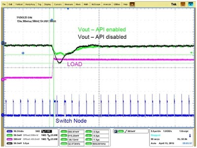
Figure 3 shows the difference with and without API based on actual bench results of the TPS543C20, a 40A device that’s capable of 80A when stacked. The test configuration was a 12V input voltage, 0.9V output voltage, 500kHz switching frequency and 15A step up/step down with a slew rate of 50A/µs. When comparing the same device with and without these features enabled, undershoot was approximately 36mV less with API enabled.

Figure 3: Undershoot with API enabled/disabled

As shown in the simulation and bench testing enabling API resulted in less deviation from the nominal output voltage during load transients, and improved the converter’s response time, when compared to API being disabled. This feature offered in the TPS543B20 and TPS543C20 devices that can reduce the amount of undershoot during a load current increase with the same amount of output capacitance, which is something to consider when designing in Arria 10 and Stratix 10 FPGAs.

You might be wondering, what about the overshoot caused by a load current decrease? These same devices offer a feature to improve transient response during a load current decrease as well. I will be taking a look at it in my next blog: Improving Overshoot of Voltage Regulators for Intel Arria 10 and Stratix 10 FPGAs.

Additional resources

10 more reasons to start using Power Stage Designer

$
0
0

Since 2011, TI’s Power Stage DesignerTM has been a great design aid for many electrical engineers when calculating the currents and voltages of different power-supply topologies. It is the easiest tool to start a new power-supply design, because all calculations are executed in real time and you get a direct feedback. With the evolution from version 3.0 to 4.0, Power Stage Designer offers three more topologies and a whole new set of features in the form of a toolbox that will help you speed up your power-supply designs even more.

The new toolbox contains a field-effect transistor (FET) losses calculator, a current-sharing calculator for parallel capacitors, an AC/DC bulk capacitor calculator, a resistor-capacitor (RC) snubber calculator for damping ringing across rectifiers, a resistor-capacitor-diode (RCD) snubber calculator for flyback converters, an output-voltage resistor divider calculator, dynamic analog and digital output voltage scaling calculators, a unit converter, and a Bode plotting tool for loop compensation. Let’s look at each of these 10 new features in detail.

No. 1: FET losses calculator

With this tool, you can easily compare different FETs that are either operating as a main switch or as a synchronous rectifier. The minimum, maximum and root mean square (RMS) current values, FET drain-source voltage and switching frequency will transfer from the chosen topology window. The tool can also help you assess the total metal-oxide semiconductor field-effect transistor (MOSFET) losses of synchronous converters after you’ve chosen applicable MOSFETs for the main switch and synchronous rectifier. Figure 1 shows the FET losses calculator window.

Figure 1: FET losses calculator window

No. 2: Current-sharing calculator

When paralleling different kinds of capacitors at the input or output of a power converter, the capacitors experience different amounts of RMS current depending on their impedance. With Power Stage Designer, you can estimate the current stress for up to three parallel capacitors based on a first harmonic impedance model.

No. 3: AC/DC bulk capacitor calculator

AC-to-DC converters typically have a bulk capacitor behind the input rectifier to provide a quasi-constant input voltage to the power stage and the power-management controller. Power Stage Designer gives you a suggestion for the bulk capacitance based on different input parameters.

No. 4: RC snubber calculator for rectifiers

In power supplies, ringing across rectifiers can be a major issue if you need to pass electromagnetic interference (EMI) testing. There are different methods to deal with this problem and implementing an RC snubber network is an easy solution that might not require you to redesign your printed circuit board (PCB) layout. Power Stage Designer gives you an easy way to determine the starting values for your RC snubber network.

No. 5: RCD snubber calculator for flyback converters

Due to parasitics like transformer leakage inductance, flyback converters can experience voltage overshoot and ringing at the switching node. The easiest way to reduce the ringing and damping of the overshoot is to implement an RCD snubber circuit in parallel with the primary inductance of your flyback converter. Power Stage Designer can help you choose starting values for the snubber resistor and capacitor.

No. 6: Output-voltage resistor divider calculator

It is now possible to easily calculate the output-voltage feedback divider for your power supply based on output voltage, reference voltage and high-/low-side resistance, including tolerances, with Power Stage Designer.

No. 7: Dynamic analog output voltage scaling calculator

For some applications, the output voltage of a power converter needs to be adjustable in a certain output-voltage range. You can accomplish this by feeding a variable analog output voltage with a third resistor to the output voltage resistor divider. Power Stage Designer helps you find the values for the resistances needed based on the chosen output-voltage range, maximum adjusting voltage, reference voltage and the top feedback resistance.

No. 8: Dynamic digital output voltage scaling calculator

It’s also possible to adjust the output voltage of your power supply by paralleling multiple resistor/signal MOSFET combinations with the low-side feedback resistor. By enabling and disabling the MOSFETs with a microcontroller, it’s as if you’ve “programmed” different output voltages to the power supply. Power Stage Designer will assist you with choosing the resistance values for the feedback circuit.

No. 9: Unit converter

Power Stage Designer provides you with a little helper that converts different power-supply parameters, such as gain to factor or imperial to International System of Units (SI), and vice versa.

No. 10: Loop calculator

The loop calculator supports you by displaying Bode plots of the open- and closed-loop transfer functions for the voltage-mode control (VMC) buck and five different current-mode control (CMC) topologies – which are buck, boost, inverting buck-boost, forward and flyback. You can use five different compensation networks for closing the loop. Figure 2 shows the Power Stage Designer loop calculator window.

Figure 2: Power Stage Designer loop calculator window

For the equations and assumptions behind the new toolbox, see the “Power Stage Designer User’s Guide.”

Additionally, Power Stage Designer 4.0 now supports a total of 20 topologies. The three new topologies in version 4.0 are:

  • Series capacitor buck converter.
  • Quasi-resonant/frequency-modulated flyback converter.
  • Inductor-inductor-capacitor (LLC) half-bridge converter.

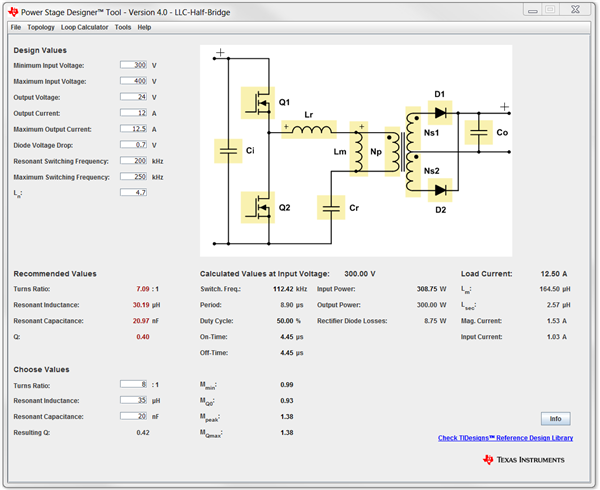
Figure 3 shows the topology window of the LLC half-bridge converter.

Figure 3: Topology window of the LLC half-bridge converter

Get Power Stage Designer 4.0 and make your life as a power-supply designer a little bit easier.

Additional resources


Use load switches for power sequencing

$
0
0

Virtually all complex processors require some kind of power sequencing at power up and/or power down. The timing requirements vary depending on processor selection and the subsystems being powered. For example, the image processor in a multifunction printer (MFP) has several rails that need to power up and power down in a specific order to properly bias the internal circuitry and stagger the in-rush current at startup. In this post, I will review different ways to implement power sequencing and the benefits of using integrated load switches to do so.

Why use load switches for power sequencing?

Load switches provide design flexibility and simple control of subsystem power sequencing. Each rail can turn on and off independently without extensive processor intervention, and the rise and fall time of each rail is adjustable. This is possible because of features available in integrated load switches such as configurable rise time and quick output discharge (QOD). TI’s TPS22918 is an example of an integrated load switch that has both of these features available. Figure 1 shows examples of common subsystems.

Figure 1: General system block diagram of MFP subsystems

Using load switches over discrete metal-oxide semiconductor field-effect transistor (MOSFET) solutions also provides improved transient behavior and smaller solution size. You can read more about these benefits in the application report, “Integrated Load Switches Versus Discrete MOSFETs.”

If you need more protection throughout your design, you can place an eFuse at the input of any hot-pluggable loads to help against hot-plug transients and protect downstream DC/DC converters from an input voltage that is too high or too low. Unlike a discrete fuse, eFuses do not need replacing after a fault, resulting in reduced system downtime and decreased maintenance costs.

Power sequencing configuration options

Power sequencing requirements are unique to each processor and system configuration. Load switches control each power rail by adjusting the timing capacitance value on the CT pin and the resistance value on the QOD pin, without the need for external digital components such as oscillators, clocks or a processor. Figure 2 shows various configurations for implementing power sequencing in your system.

Figure 2: General-purpose input/output (GPIO) configuration

Figure 2 uses independent enables for each load switch to trigger power-up sequencing. Varying the resistance on the QOD pin achieves power-down sequencing.

Figure 3 uses one GPIO signal to enable all three load switches, but varies the capacitance at the CT pin to control power-up sequencing. Again, varying the resistance on the QOD pin achieves power-down sequencing.

Figure 4 routes the QOD output of the previous load switch to the enable pin of the next load switch. Adding an external resistor-capacitor (RC) in parallel to the QOD output achieves power-up sequencing. Once more, varying the resistance on the QOD pin achieves power-down sequencing.

Figure 4: QOD configuration

You can learn more about implementing power sequencing in your designs from TI’s Power Sequencing Reference Design Using Load Switches. Since timing constraints vary greatly between different applications and processor-to-processor communications, this reference design is not limited to one specific timing sequence. Instead, the design enables you to configure multiple timing configurations to fit system specifications.

Additional resources

How to Select a MOSFET – Selection Tool

$
0
0

In my last blog post, I talked about how difficult it can be to select the most appropriate field-effect transistor (FET) for switch-mode power supply (SMPS) applications. Predicting circuit performance from a data sheet specification is a tedious process. To get an idea of how tedious, I recommend reading the application note “Power Loss Calculation With Common Source Inductance Consideration for Synchronous Buck Converters,” as it meticulously details the power-loss impacts of first and second order parasitic elements for this one specific topology.

Now, thanks to the Online Design Tools team, TI offers a nifty web-based tool to help you weigh the cost and performance trade-offs for various metal-oxide semiconductor field-effect transistors (MOSFETs). The tool uses the equations from the aforementioned application note, and thus only specifically covers a synchronous buck converter topology. However, because this topology is overwhelmingly the most popular non-isolated DC/DC topology for implementing discrete FETs, it still supports a vast array of power-supply end applications.

Basically, the tool works as follows. First, a user will select from a list of TI controllers, or build their own controller by entering custom parameters (Figure 1). Then they will enter the various application conditions (input voltage, output voltage, output current and switching frequency if the controller supports that option). And that’s it! From there, the tool does all of the calculations for you!

Figure 1: Using this interface, you can input your end application’s parameters and controller

Once the submit button has been clicked, the tool will determine the minimum FET breakdown voltage that will support the input voltage and rank all potential TI FET solutions by power loss (Figure 2). The higher on the list, the less the power loss for that socket.

Figure 2: Solutions for the input parameters shown in Figure 1 ranked by power loss

The ranked solutions include a list of discrete options as well as power block solutions – a single half bridge vertically integrated into one package. Why would you be interested in power block solutions? In addition to the reduced-footprint and power-density advantages, their stacked-die silicon technology enables an optimized thermal layout and much lower parasitic source inductance compared to two discrete FETs. The application note makes the case that parasitic source inductance can have a significant contribution to total system switching losses, particularly as you drive to higher frequencies. So it’s important that the NexFET power MOSFET selection tool is intelligent enough to account for the secondary effects of common source inductance (LCSI) when calculating loss, because doing so effectively shows some of the measurable advantages of a power block.

I’d like to make a few last points on how the tool should and should not be used. It is most effective as a mechanism for the relative comparison of loss and price (and maybe size). It enables you to quickly assess the trade-offs between solutions firsthand and make the decision most appropriate for you. As an example, let’s refer back to Figures 1 and 2. At first glance, you might select the CSD86330Q3D power block because it is the most efficient of any solution (based on lowest power loss). But look one row down at the CSD87331Q3D and you’ll see a solution that, while 4% higher in total losses, is also 34% cheaper (at 1k quantities). On top of that, the CSD87331Q3D has a 30V breakdown voltage (BVDSS) which will enable greater margin over your 18V input relative to the 25V CSD86330Q3D. Or maybe the designer doesn’t care that the SON3x3 package is smaller; they might be worried about dissipating ~2W into the smaller package due to their end equipment’s hard thermal environment. In that case, maybe they would select the 5mm-by-6mm CSD87352Q5D. The point is that the tool empowers the designer to make the decision themselves.

Under no circumstances should a user assume that the tool is 100% accurate with respect to the loss they will see on your board, because other factors that the tool cannot predict (ambient temperature, board layout considerations) will also impact that final value. Before releasing the tool, the Online Design Tools team did several verification studies and found that predicted losses compared to measured losses were usually within 5-10% – but predicting loss with absolute certainty is not the intention of the tool.

On that point, the tool does remove devices from its ranked recommendations only based upon breakdown voltage considerations. It gives plenty of freedom to design something wildly impractical if one so chooses. For example, there is nothing inherent in the tool that would advise against dissipating 10W of power into a single SON5x6 FET while switching at 10MHz, but good luck trying to get that to work on a real board without melting the printed circuit board (PCB). Although the tool is great at reducing the amount of time and effort that goes into predicting the power loss of dozens of solutions simultaneously, some intelligence on the user’s side is still required to produce a stable design.

I hope you’ll get a chance to play around with this tool the next time you need to select a FET (or power block) device for a buck application, and that you find it as useful and timesaving as I do.

Additional resources


Powering FPGAs – improving overshoot of voltage regulators for Intel Arria 10 and Stratix 10 FPGAs

$
0
0

Previously, in my last blog “Improving undershoot of voltage regulators for Intel Arria 10 and Stratix 10 FPGAs” we discussed how Asynchronous Pulse Injection (API) could reduce the undershoot of a fixed frequency DC/DC converter during a sudden increase in load current. Now I would like to discuss a feature that helps address the overshoot needs of the Arria 10, Stratix 10, or similar FPGAs. Overshoot reduction is critical for digital point of loads such as the Arria 10 and Stratix 10 because excessive supply voltage can stress or even damage sensitive, high-speed circuits.

First, let’s understand how fixed frequency DC/DC converters respond to a sudden decrease in load current in order to maintain the regulated output voltage. In order to limit the amount of rise in output voltage, the low-side field-effect transistor (FET) of the converter turns on in order to sink the voltage. During this time, the voltage across the inductor is very close to the actual output voltage. Equation 1 computes the voltage across the inductor with the low-side FET on:

where  is the inductor voltage with the low-side FET on, VOUT is the output voltage, IL is the inductor current, DCR is the DC resistance of the inductor, Rtrace is the trace resistance of the printed circuit board (PCB) and RDS(on) is the drain-source resistance of the low-side FET.

Equation 2 defines the rate at which the current drops:

Equation 3 defines the total charge that the output capacitor must absorb during a load step down:

where  is the load-transient step size.

Now consider what would happen if instead of turning the low-side FET on during a sudden load current decrease, you turned it off. This feature is known as overshoot reduction (OSR), or “body brake.” By turning off both the high- and low-side FETs during a rapid load current decrease, you can limit the amount of overshoot.

Let’s look at what happens to the flow of current when the low-side FET turns off and reevaluate Equation 1, which computed the voltage across the inductor. Figure 1 shows the current flow when the low-side FET is turned off, in which the current flows out of the inductor into the output capacitor, out of the output capacitor into ground, out of ground and through the body diode of the low-side FET, and back to the inductor.

Figure 1: Current flow during OSR

Equation 2 computed the voltage across the inductor with the low-side FET on. What happens to this equation when the low-side FET is off? RDS(on) is no longer a factor, but the forward voltage drop of the low-side FET body-diode is, as shown in Equation 4:

Since the voltage drop across the body diode of the low-side FET is greater than the conduction channel (IL x Rdson), you can see that:

Therefore, VLLS_OFF results in a larger, negative voltage across the inductor. This larger negative voltage causes the inductor current to slew down faster, resulting in less total charge flowing into the output capacitor (replacing VLLS_ON with VLLS_OFF in Equation 3) and producing less overshoot. 

Now let’s look at a simulation of a model with and without OSR enabled. Table 1 shows a common rail voltage rating for Arria 10 field-programmable gate arrays (FPGAs).

Min

Typ

Max

Unit

0.92

0.95

0.98

V

Table 1: Common voltage ratings for VCC, VCCP, VCCERAM and more for Arria 10 FPGAs

Figure 2 shows a load-transient simulation of a fixed-frequency converter without OSR. The load current, or the lower waveform in Figure 2, steps down. As a result, the output voltage, or the upper waveform in Figure 2, rises above the required maximum operating voltage labeled “max” at 0.98V.

In addition to the required maximum and minimum values for this particular rail, there is a percentage of error associated with the actual output voltage of the power supply when compared to the target voltage. Two devices that offer OSR, the TPS543B20 and TPS543C20 from Texas Instruments, have an adjustable reference voltage with 0.5% accuracy that you can set to the target output voltage of 0.95V. This means that you can improve the percentage of output voltage accuracy error by removing the deviation caused by the tolerance of the feedback resistor divider. The resulting output voltage accuracy error percentage is approximately ±0.5%. This decreases the amount of available tolerance by ±4.75mV, which is also shown in Figure 2, labeled “Max w/ %Error” at 975mV.

Figure 2: A load-transient simulation of a fixed-frequency converter with OSR disabled

Figure 3 shows a load-transient simulation of a fixed-frequency converter with OSR enabled. The upper waveform in Figure 3 is the output voltage, which now remains within the operating range of the expected voltage values listed in Table 1 labeled “Min,” as well as the minimum when accounting for output voltage accuracy labeled “Min w/ %Error” at 975mV. The middle waveform in Figure 3 is the switch node; you can see that the load current, or the lower waveform in Figure 3, steps down at the same point with respect to the switching cycle compared to the previous simulation. Both the high- and low-side FETs are off.

Figure 3: A load-transient simulation of a fixed-frequency converter with OSR enabled

Figure 4 shows the difference with OSR (body brake) enabled and disabled on actual bench results of theTPS543C20. The test configuration was a 12V input voltage, 0.9V output voltage, 500kHz switching frequency and 15A step up/step down with a slew rate of 50A/µs. When comparing the same device with and without this feature enabled, the overshoot was approximately 49mV less with OSR enabled.

Figure 4: Overshoot with OSR enabled/disabled

Table 2 lists two devices currently available with OSR and asynchronous pulse injection (API) used to limit undershoot, as well as a few key features for these devices. These devices offer API adjustability and the ability to enable or disable API and OSR.


TPS543B20

TPS543C20

API

Yes

Yes

OSR

Yes

Yes

High-side FET RDS(on)

4.1mΩ

3mΩ

Low-side FET RDS(on)

1.9mΩ

0.9mΩ

Current rating

25A

40A-80A*

Comments


*Device is stackable up to two phases

Table 2: DC/DC buck converters that include API and OSR

Using Texas Instruments devices with the features listed here showed improvement in regards to the total amount of undershoot and overshoot when compared to having these features disabled. With these features, you can meet voltage regulation requirements with less output capacitance, which is something to consider when designing in Stratix 10 and Arria FPGAs.

Additional resources


Improving the thermal performance of a power module

$
0
0

A derating curve like the one shown in Figure 1 is an essential part of making a power module easy to use. With the derating curve, you can quickly see if the power module is rated to support your particular application’s requirements. In most cases, the derating curve shows the rated output current at various ambient temperatures. Operating below this line operates the power module within its temperature, power and/or current limits.

Figure 1 shows several derating curves for a MicroSiP power module, each for a different value of the junction-to-ambient thermal resistance, commonly known as ΘJA. Wouldn’t you choose the power module that produces the green curve, since it has the lowest ΘJA and the least derating?

Figure 1: Derating curve for the a MicroSiP power module


Actually, each curve in Figure 1 uses the same TPS82130 power module under the same operating conditions. Only the printed circuit board (PCB) layout and airflow have changed. You, the designer, choose which derating curve you get. This brings to light a key truth about power modules: their thermal performance, and thus their derating, is highly dependent on the application and usage of the device, which includes the PCB layout and system variables such as airflow.

Specifically, the red curve in Figure 1 is generated with the standard Joint Electronic Devices Engineering Council (JEDEC) PCB design. While JEDEC’s board definition is used to generate most thermal tables in device data sheets, the JEDEC board is not a very realistic type of board for final applications.

Figure 2 shows one difference, of many, between the JEDEC PCB and a more typical application PCB: the amount of copper connected to the device’s pins. The very small amount of copper (shown in purple) used in the JEDEC design yields unrealistically poor thermal performance.

Figure 2: The JEDEC PCB uses very thin amounts of copper connecting to the device’s pins

By focusing on the thermal design when using a power module, it’s possible to easily achieve better performance than the JEDEC PCB. Table 1 shows several design options using different numbers of vias, layers and airflow. All are an improvement over the JEDEC PCB design, quantified by the lower ΘJA value and resulting lower operating temperature. Just through PCB and system design, you can reduce the operating temperature by nearly 50°C.

Table 1: Thermal-performance comparison of different PCB designs

Want to read more about this topic? Check out my article, “Improving the thermal performance of a MicroSiP power module,” in the Analog Design Journal.

How to Select a MOSFET – Load Switching

$
0
0

“Two roads diverged in a yellow wood, marked FemtoFET and SOT-23,

So I chose the path of FemtoFET to shrink my PCB”

 – Robert Frost (I think)

MOSFETs are being used as load switches more than they are being used in any other application, in volumes in the hundreds of millions at a time. I should probably start with exactly how I am defining “load switch” here. For the sake of this post, consider a load switch any small-signal FET whose only function in a system is to pass along (or block) some low-current (<1A) signal to another board component. Battery-protection MOSFETs have very similar functionality, but represent a unique subset of load-switch applications that can also carry much higher currents.

Our applications team has a word for load switch FETs – “pixie dust” – to describe the somewhat ubiquitous way that they can be “sprinkled” over a system after most of the design is complete. That perhaps does these tiny powerhouses a disservice, in that they are also often the glue that holds the electronic system together.

The small signals that these devices carry are generally on the order of a few hundred milliamps such that in theory, there is no reason that the function can’t be integrated. However, custom integrated circuits (ICs) are often more costly than they are worth, such that once a design is complete, it is easier to implement a few of these small signal FETs rather than requesting or redesigning a custom IC. Given that, there are typically two fundamental requirements for these devices: that they be cheap and small. Which of these requirements is the most critical will dictate what type of MOSFET is most appropriate for your design.

If cost is the most important factor, small-form-factor packages like the small-outline transistor (SOT) series (SOT-23, SOT-26, SOT-323, SOT-523) will be the most preferable option. These devices have a PCB footprint from 2.6mm2 to 10mm2, on-resistances in the range of several hundred milliohms to a few ohms, and can handle currents up to roughly half an amp (depending on the resistance). They are comprised of large protruding leads and a somewhat bulky package (see Figure 1). While some industrial designers prefer the external leads, as they make for simple board mounting and enable easy visual inspection for a solder connection, the strongest appeal of these FETs is their low cost (think a penny or less). I should note that TI really doesn’t have any offerings for MOSFETs in these packages, or intention to play in this commoditized space. 

Figure 1: Several SOT packages (not drawn to scale)

On the other hand, if reducing the PCB space taken up by many extraneous small-signal transistors is the biggest concern, a better solution is either a bare-die chip-scale package (CSP) or land grid array (LGA) device. TI carries a wide variety of these types of devices, the most popular being from our FemtoFET product line (Figure 2). These devices have an ultra-small footprint, offering size options all the way down to just under 0.5mm2. This tiny form factor inevitably means high junction-to-ambient thermal impedance through the PCB. However, with resistances that can be one to two orders of magnitude less than the larger-footprint SOIC package devices, the reduced conduction losses more than make up for the slight increase in thermal impedance, enabling higher current-handling capability in some cases greater than 1A.

Figure 2: Three different FemtoFET package offerings (not drawn to scale)

Before selecting which of the above roads to travel down, I offer two final caveats. The first is that before committing to a FemtoFET (or some other ultra-small device), you should check your PCB manufacturing capabilities. Some industrial manufacturing processes prefer a larger pitch between mounting pads (hence the preference for SOT devices). Others can handle pitches down to 0.5mm (like the F5 FemtoFET family), while personal electronics manufacturers can often handle pitches down to 0.35mm (supported by the F4 and F3 FemtoFET packages).

I’ve spoken at length about current ratings before, but because the sole purpose of a load switch is to carry small currents, it’s worth revisiting one more time. As usual, the best practice is to ignore the front-page current ratings, and instead work backwards from how much power loss you think your system will permit the FET to dissipate.

Most data sheets will provide a junction-to-ambient thermal impedance (RθJA) for a minimum and maximum copper (Cu) PCB scenario. Using the minimum Cu as a worst case is the safest bet, although if you know the end board dimensions, you could try to interpolate an RθJA between the minimum and maximum Cu impedances provided on the data sheet. Then, using Equation 1 below, and knowledge of the end equipment’s worse-case ambient environment, you can calculate how much power the FET can handle, and therefore current as well:

One nice thing about load-switch applications is that the device is either on or off. Therefore – unlike all the other applications I’ve discussed to this point in this series – all of the power losses are due to conduction losses (I2R).

Thanks for reading. In the next post, I’ll take a more in-depth look at a subset application of load switches that I mentioned at the beginning: FETs used for battery protection.

Additional resources

TI empowers design engineers at APEC

$
0
0

Join Texas Instruments at the Applied Power Electronics Conference (APEC), March 4-8, in San Antonio, Texas to experience the latest innovation in key applications, interactive design stations and advice from our experts.

If you’re not attending in person, follow this blog for real-time updates and monitor us on social media for the latest:

Visit our booth #501 to see new products and end-to-end power-management system solutions including hardware, software and reference designs that give designers the power to:

Innovate:

  • The Industry’s Fastest and Most Efficient CrM Totem-Pole PFC Design: This critical conduction-mode reference design features TI’s 600V GaN power-stage technology and Piccolo™ F280049 controller to achieve up to 99% efficiency at full load. The 1MHz, high-density-interleaved 1.6kW design is ideal for space-constrained applications such as server, telecom and industrial power supplies. Interleaving the power stages reduces input and output ripple currents. The hardware of this device is designed to pass conducted emissions and surge requirements, helping designers achieve 80 Plus Titanium specifications. Download the TIDA-00961 reference design.

Design:

  • Get to market faster – WEBENCH® Power Supply Design tool: Analyze and interpret designs with WEBENCH Power Design tools. Go beyond the traditional concerns of performance, footprint and cost with tools that mitigate electromagnetic interference (EMI) noise and handle noise-sensitive loads. Start a design now at TI.com/WEBENCH.
  • Work smarter, not harder - Power Stage Designer ™ tool: Power Stage Designer™ is a JAVA based tool that helps engineers accelerate their power-supply designs by calculating voltages and currents of 20 topologies according to the user’s inputs. Additionally, Power Stage Designer contains a Bode plotting tool and a toolbox with various functions to make power supply design easier. Because all calculations are executed in real time, this is the quickest tool to start a new power supply design. 

Learn:

  • Join TI at technical sessionsJoin TI power experts at more than 30 technical sessions covering topics such as renewable energy systems, wireless technology and GaN device reliability validation. 
  • Power up: 6 power management trends to address growing energy requirements: Circuit designers are seeking innovative technologies to address power-management challenges presented by fast-growing global energy consumption. Read the blog to see the 6 trends addressing some of their toughest requirements.
  • Power waveforms and equations and more, oh my!: Download the Power Topologies Handbook for waveforms and equations of the most common hard switched power supply topologies and the soft switched Phase-Shifted Full-Bridge.
  • Get a TI Power Management Lab KitCheck out the TI Power Management Lab Kit (TI-PMLK) buck-boost board and experiment book to better understand the trade-offs related to common power-supply parameters such as power losses, converter efficiency, stability, load and line regulation, and more.

Should you power your industrial sensors with a linear or switching regulator?

$
0
0

Modern factories feature automated systems that rely on feedback from many sensors across the factory floor to maintain high productivity. These factories use a digital fieldbus to aggregate the enormous amount of data that the sensors collect. The more data that the sensors gather, the better the system can adapt and operate.

As a result, modern fieldbus-connected industrial sensors must detect signals at a faster and more precise rate and output that information as a digital signal versus a conventional analog signal. This functionality requires more powerful processors for the sensors. Plus, because there are more of these sensors in the factory, the form factor is shrinking. The increased power requirements and shrinking form factor are forcing a change from the proven linear regulator solution to a switching regulator solution.

Using a switching regulator poses new challenges. A switching regulator will have a larger form factor because of the additional area that the inductor requires. You must consider the regulator’s switching frequency in relation to the frequency of the measurement signal.

The layout of the switcher is more critical. A poorly designed switching regulator will raise the noise floor and generate unwanted electromagnetic compatibility (EMC) that will interfere with the detection of small signals.

Fortunately, there are now integrated inductor DC/DC switching regulators available that minimize many of these challenges. Integrating the inductor reduces the switch-node area and makes an optimal layout much easier. The switching frequency of new DC/DC converters has increased significantly, enabling the use of small-chip inductors and ceramic capacitors to make the DC/DC switcher the smallest option.

The new LMZM23601 power module integrates a DC/DC converter, inductor, Vcc filter capacitor and boot capacitor in a 3mm-by-3.8 mm-by-1.6mm package. It can handle input voltages up to 36V and steps down to voltages from 15V to 2.5V (with fixed 5V and 3.3V options) while delivering up to 1A of output current. As you can see in Figure 1, you can realize a complete 1A solution in a minimal amount of board space.

Figure 1: The LMZM23601 solution for 3.3V or 5V outputs at up to 1A

Let’s take a look at how the LMZM23601 compares to the traditional linear regulator options for a field transmitter application with these requirements:

  • Input voltage: 10V to 30V, 24V nominal.
  • Output voltage: 3.3V.
  • Output current: 35mA.
  • Temperature range: -40°C to 85°C ambient.
  • Board area: 40mm by 4.5mm.

As Table 1 shows, the LMZM23601 is at an advantage in terms of package area and thermals compared to a linear regulator in a mini small-outline package (MSOP)-8. Note that the RӨJA specified in Table 1 is only a reference for comparison, since it will be much higher in an actual sensor application given the limited amount of board space and copper. A Joint Electron Device Engineering Council (JEDEC) or an evaluation module (EVM) calculates the typical RӨJA value found in the data sheet. As an example, the LMZM23601 RӨJA of 45°C/W is based on a 30mm-by-30mm two-layer board.

Design option

Package footprint (mm)

Package area (mm2)

Package thermals

RӨJA (ᵒC/W)

LMZM23601

3 x 3.8

11.4

45

Linear – MSOP-8

5 x 3

15.0

60

Linear – heat-sink thin-shrink small outline package (HTSSOP)

5.1 x 6.6

33.7

39.7

Linear – transistor outline (TO)-252

10.7 x 15.9

169.4

26.9

Linear – TO-263

10.4 x 6.7

69.7

24.7

Table 1: LMZM23601 vs linear regulator design options by package type 

Looking at Table 2, the linear regulator is dissipating (24V-3.3V) x 35mA = ~0.93W of power, while the LMZM23601 is dissipating only 0.116W. The temperature rise in the MSOP-8 package linear regulator results in a junction temperature above the standard integrated circuit (IC) junction temperature of 125°C, while the junction temperature for the LMZM23601 is 90°C based on a 45°C/W RӨJA. Even multiplying the RӨJA by a factor of five would still yield a Tj max below the junction temperature.

Design option

Power dissipation (W)

Temperature rise

(°C)

Junction temperature

(°C)

LMZM23601

0.1155

5.2

90

Linear – MSOP-8

0.9355

56.13

141


From this example, it is clear that a linear regulator is not a viable option in terms of thermals. The trade-off of going with a switching solution (even a module such as the LMZM23601) is that you now must consider the output ripple. As shown in Figure 2, the output ripple from a standard LMZM23601 design for a 3.3V output is about 3mV peak to peak.
Table 2: Thermal considerations for a 24V-to-3.3V conversion at 35mA

Figure 2: Output ripple from the LMZM23601EVM for a 3.3V output

To further reduce the output ripple, you can use a second-stage filter like the one shown in Figure 3. Figure 4 shows that the output ripple has been reduced from 3mV peak to peak to <1mV peak to peak.

Figure 3: The LMZM23601 with a second-stage filter


Figure 4: LMZM23601 output-voltage ripple with a second-stage filter

For industrial sensors with tight board space requirements, a switching regulator is the only viable option. The LMZM23601 integrated inductor delivers high performance in a solution size smaller than a linear regulator, but with the efficiency of a switching regulator.

Additional resources


Why you should use a dedicated fuel gauge in your battery management system

$
0
0

Anyone who uses a battery-powered product or device can appreciate the importance of an accurate battery-capacity indicator. It can be very frustrating to have your device suddenly die without any warning.

Traditionally, the simplest method of indicating battery capacity was to measure the battery voltage with an analog comparator and generate a simple low-battery warning below a predetermined threshold. In products that already have a general-purpose microcontroller (MCU), an analog-to-digital converter (ADC) can make a more accurate (digital) voltage reading, compare that reading to a set of predefined levels, and generate a more sophisticated battery-level indicator.

But if you look at the voltage profile of an actual battery in an application with variable load conditions, you will soon learn that a simple voltage-based reading can be very misleading. Assume that a single-series cell-powered system needs to be alerted when the battery voltage is 3.7V, which is based on an open circuit voltage (OCV) of about a 15% state of charge (where 0% is empty and 100% is full). The challenge is that battery voltage may cross 3.7V several times before settling. The system may alert the end user too early and shorten the run time or issue an alert too late and allow the system to crash, potentially even damaging the hardware.

Figure 1 is an example of the same battery responding to dynamic loads at different temperatures. Using a lower current at cold temperatures helps drain out all of the battery’s capacity. The depth of discharge (DOD) (DOD = 1 – true state of charge) normalizes the X axis. The voltage responses appear to be two different animals!

Figure 1: Battery-voltage response to dynamic loads at different temperatures

Aging is another concern. Once the present full capacity of the battery is below 80% of its original full capacity due to aging, it’s going to spiral down to its end-of-life state very quickly. For an aged battery, a voltage = 3.7V may indicate almost no remaining capacity.

In many cases, a generic MCU’s ADC accuracy is typically not good enough for an accurate state-of-charge calculation. For some batteries, 1mV error converts to a 1% state-of-charge error. Figure 2 is an example where ±20mV accuracy means a 20% state-of-charge error in the flat region, assuming that you need OCV.


Figure 2: DOD percent error caused by OCV reading error

Furthermore, the general-purpose MCU in a system may have many functional blocks and numerous other tasks going on in parallel. It may not be the most power-efficient solution or the most accurate battery-level indicator. But by adding a small external application-specific fuel-gauge device, you can get a more accurate and power-optimized solution.

If the portable device spends a significant amount of time in an idle/low-power state, the main MCU (which could consume more power than a dedicated gauge device) does not have to wake up and consume power just to check on the battery condition. While it can take the MCU several milliamps to measure and calculate the state of charge, a discrete gauge consumes only a small fraction of what an MCU would have consumed– the average current is 20 to 30µA with sleep mode on. With proper power-management techniques, it can even drop to <2µA.

TI’s discrete gauge hardware is specifically designed for battery management. The gauge device takes accurate measurements with minimum power consumption. However, without a proper battery model and supporting gauge algorithm, the measurements are only a reflection of the present moment. The TI models and gauge algorithm comprehend the electrochemical features of many different kinds of batteries and have been proven in many millions of systems in the field.

In addition, TI discrete gauges provide added functionality such as black-box battery forensics, health indication and smart charge control. An accurate gauge device helps bring power management to another level for an enhanced customer experience.

Last but not least, a percentage prediction adds sophistication and intelligence to the product, and instantly improves the end-user experience.

If you’re trying to find the right fuel gauge to your design, try searching our portfolio of gauges.

Additional resources


How to increase charging current by 50% with half the size in portable electronics

$
0
0

Modern portable electronic devices include a high-capacity lithium-ion battery to power the features we know and love, such as high-definition cameras, edge-to-edge high-resolution touchscreens and a high-speed data connection. As the list of features continues to increase, so does the battery capacity required to support them, along with the charge current required to recharge the battery in a reasonable amount of time.

One key consideration for system designers is balancing battery capacity, charging time and device temperature while charging. This last element is important, not only to enhance the user experience but to improve battery safety and lifetime. Given a battery’s capacity, you can reduce the charging time by increasing the charging current, while controlling the equipment temperature by reducing the total power loss inside the device.

Switch-mode battery-charger efficiency typically drops at higher current levels, which translates to a larger power loss and higher equipment temperatures. A buck-based battery charger can typically achieve higher efficiency by sacrificing solution size; for example, a larger inductor with a lower resistance might increase the efficiency of a typical design at high currents.

TI’s latest companion battery charger, the bq25910, is based on a three-level buck converter technology, which gives you the flexibility to increase efficiency by 5 percentage points while shrinking the solution size by 2x. This is an exceptional improvement in efficiency and solution size, and translates to a 50% increase in charge current for a fixed loss budget when compared to the older generation chargers.

The three-level buck converter illustrated in Figure 1 is a combination of a switched capacitor and switched inductor circuit with no fundamental duty-cycle limitation. With the addition of a flying capacitor, CFLY, balanced at VIN/2, the circuit reduces voltage stress on switching MOSFETs by half, doubles the effective switching frequency at VSW and reduces the volt-seconds across the inductor by half. The gate-driving scheme is similar to that of a two-phase buck converter. A complementary signal drives the outer FETs, QHSA and QLSA, with duty cycle D = VOUT/VIN. A second complementary signal of equal duty cycle drives the inner FETs, QHSB and QLSB, but is phase-shifted by 180 degrees.

Figure 1: The three-level buck converter circuit used in the bq25910 (a); the device’s total solution size is 56mm2, including all power components (b)

Assuming that CFLY remains balanced at VIN/2, the VSW node can be presented with three different voltages: VIN, VIN/2 and GND. The reduced voltage across the inductor dictates the ripple current in the circuit, which is a key parameter in selecting the required inductance. Because the inductor is typically the largest physical component of a switching converter, reducing its requirements translates to significant savings in solution size. This makes new applications possible such as height constrained, high charge current designs. Moreover, a smaller inductance will actually yield lower losses, hence the higher overall efficiency.

The addition of a flying capacitor allows the three-level buck converter to reduce switching losses in semiconductor devices as well as the size and loss of the external inductor, dramatically increasing efficiency. Even a small efficiency improvement can translate into a higher charge current, as explored by my colleague Fernando Lopez Dominguez in his blog post, “How 1.2% more efficiency can help you charge faster and cooler.” By improving efficiency by 5 percentage points, the bq25910 offers an increase in charge current from 2.9A to 4.35A for an equal power loss of 1.5W, all while reducing the total solution size 2x. You can see this illustrated in Figure 2, which compares the efficiency, size and temperature of the bq25910 to previous-generation chargers.

Figure 2: The bq25910 has +5% higher efficiency and +50% higher current for fixed losses (a); and runs 8°C cooler at half the size (b)

With each new generation, our portable electronic devices are becoming more feature-rich. These new features require both a larger battery capacity and a larger physical area to provide an enhanced user experience. This, in turn, places stringent requirements on battery chargers: they must occupy less space and charge a larger battery in an equal or shorter timeframe. The fact that buck converter-based chargers typically trade off efficiency for size requires a new technology that can provide both.

The bq25910 offers considerable improvements in fast and cool battery charging, all while reducing solution size. Consider taking advantage of this innovative solution in your next battery charger design with high current and high efficiency requirements. Order a bq25910 evaluation module today to enhance your next design with this truly innovative solution. 

You can explore the bq25910 and learn about other ways TI is giving engineers the power to innovate, design and learn by visiting booth No. 501 at the Applied Power Electronics Conference (APEC) in San Antonio, Texas, March 4-8, 2018.

Additional resources

Intelligently control an active clamp flyback

$
0
0

When I first got into cooking, I preferred to do it alone, thinking that having anyone else in the kitchen was a distraction. But as I started to cook more complicated recipes with multiple steps, I found that having a second pair of hands was invaluable and made the experience more fun. The saying is true: if you can’t beat them, join them.

The same principle applies with the active clamp flyback.

Everyone wants a smaller AC/DC converter, especially when it’s for their phone or tablet charger. Due to its simplicity, the flyback converter is the topology of choice, since it effectively converts AC to DC with few components. But there are limits to how small a flyback can be, since the losses associated with the leakage inductance of the transformer limit the practical size. Until now, every design has fought it by minimizing this leakage inductance.  But the active clamp flyback breaks this cycle.

Figure 1: Active clamp flyback with leakage inductance in red and active clamp in blue

Rather than fighting the leakage inductance by dissipating the energy in a resistor-capacitor-diode (RCD) or Zener clamp, an active clamp stores the energy and delivers it to the output. Intelligently controlling the clamp also provides zero voltage switching. This eliminates two major sources of loss, enabling the size to be drastically reduced. If you were to use gallium nitride (GaN) field-effect transistors (FETs) with their lower output capacitance and on-state resistance, the size of the adapter can be cut in half!

But the devil is in the details, since if the active clamp is not intelligently controlled, it will actually make the efficiency worse. The active clamp flyback had been only a pipe-dream, since there was no controller intelligent enough to enable this topology. But this has changed with the UCC28780. This active clamp flyback controller is specifically designed to work with silicon (Si)- or GaN-based power stages, making this topology a reality for any design. The UCC24612 synchronous rectifier enables compliance with U.S. Department of Energy (DoE) Level VI or Code of Conduct (CoC) Tier 2.

You can explore the UCC28780 and UCC24612 and learn about other ways TI is giving engineers the power to innovate, design and learn by visiting booth No. 501 at the Applied Power Electronics Conference (APEC) in San Antonio, Texas, March 4-8, 2018.

Additional resources


Maintain a constant phase margin in a synchronous buck converter

$
0
0

When designing a step-down buck converter, converter stability should be a top priority. The converter is stable when the phase margin of the loop gain is greater than 0 degrees, with an acceptable minimum phase margin of 45 degrees.  Maintaining a constant phase margin when the power-stage components vary as much as 50% from their original values can be a challenge for circuit designers.  For example, the values of the inductor and capacitors change with their bias operating conditions and temperature range.

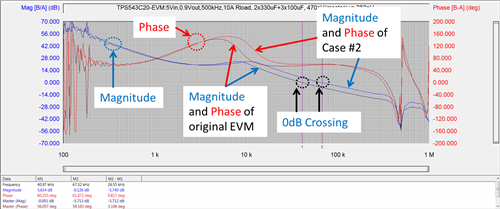
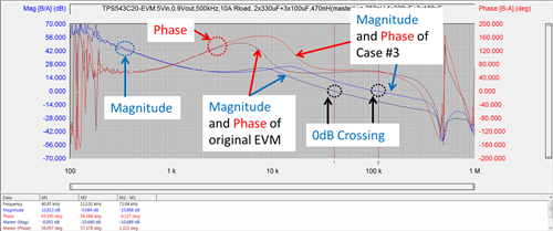
Using the new advanced current mode (ACM) control topology in TI’s TPS543C20 synchronous step-down SWIFT™ converter, I compared the shape of the phase in three separate cases. In each case, I change the value of the output capacitor, inductor and both the output capacitor and inductor without making any other modifications to the circuit. I used the single-phase TPS543C20EVM-799 evaluation module (EVM) to perform the comparison under these test conditions:

  • Input voltage = 5V, output voltage = 0.9V, switching frequency = 500kHz.
  • Original inductor value = 470nH (0.165mΩ direct current resistance [DCR]).
  • Original output capacitor = 2 x 330µF (3mΩ equivalent series resistance [ESR]) + 3 x 100µF (1206 size ceramic capacitor).
  • Output load configured as a 10A resistive power resistor.

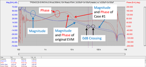
Case No. 1, illustrated in Figure 1

I compared the phase from the original default EVM to a new output capacitance value of 1 x 330µF (3mΩ ESR) + 3 x 100µF while keeping other conditions the same. As you can see, the shape of the phase very much stays the same as the original values. The phase is also basically staying constant over a decade of frequency after the double-pole frequency of inductor and output capacitor.

Figure 1: Bode plot comparison between original configurations versus case No. 1

Case No. 2, illustrated in Figure 2

I compared the phase of the original default EVM to a new inductor value – 250nH (0.165mΩ DCR) – while keeping the other conditions the same. Again, the shape of the phase is very much the same as the default configuration. The phase is basically staying constant over a decade of frequency.

Figure 2: Bode plot comparison between original configurations versus case No. 2

Case No. 3, illustrated in Figure 3

I compared the phase of the original default EVM to a combination of case Nos. 1 and 2 – 250nH (0.165mΩ DCR) and 1 x 330µF (3mΩ ESR) + 3 x 100µF – while keeping the other conditions the same. Again, the shape of the phase stays constant at 0dB.

Figure 3: Bode plot comparison between original configurations versus case No. 3

The shape of the phase in the ACM topology stays constant over a decade frequency range when the power component changes its value, such as a 53% inductor reduction from 470nH to 250nH.  However, you still need to pay attention to the changing value of power-stage components so that the phase margin of your converter meets the minimum requirement.

Additional resources:

GaN drivers – switching faster than today’s technology

$
0
0

It feels like we are living in a high-speed world, full of technology with a constantly growing demand for higher and faster performance.

Power engineers are at the forefront of this battle, developing solutions that are smaller, faster and more efficient than ever before. In applications like light detection and ranging (LIDAR), older-generation solutions only operated in hundreds of kilohertz. Newer platforms requiring longer ranges and increased accuracy need to be 10 times faster, with laser pulses below 5ns.

To achieve nontraditional performance, you need nontraditional technology. Only gallium nitride (GaN) can provide speed that fast with optimal performance. But to really harness the power of GaN, you need a driver capable of handling those frequency levels.

A very high switching frequency is necessary for next-generation telecom infrastructures like 5G envelope tracking, a key power method that ensures that the power amplifier is operating at peak efficiency during each point of transmission. Figure 1 shows losses from traditional supply-voltage methods compared to GaN-enabled envelope-tracking methods.

Figure 1. Traditional supply-voltage methods

TI’s Multi-Megahertz GaN Power Stage Design for High Speed DC/DC Converters, featuring the LMG1210 half-bridge GaN driver, enables 50MHz operation and optimized efficiency capability through adjustable dead-time control for the highest efficiency in 5G communication.

The driver’s ability to control dead time is a key design parameter in high-frequency converters, and is especially important as the frequency of operation increases. The device’s integrated dead-time control function allows you to fine-tune your design for best efficiency.

LIDAR is giving eyes to our technology, for detection, monitoring and mapping applications. But engineers need the fastest possible laser drivers to achieve high-resolution in LIDAR vision. The Nanosecond Laser Drive Reference Design for High Resolution LIDAR features the LMG1020 low-side driver; its 60MHz/ns performance provides sub-nanosecond pulses for the best performance in LIDAR laser applications. The increased power density in the industry’s smallest GaN driver enables extended range for industrial LIDAR vision, while short pulses comply with infrared (IR) laser eye safety standards.

5G envelope tracking, LIDAR, along with others, require excellent high-speed performance only enabled by GaN. TI’s GaN portfolio of products, including GaN drivers, gives you the speed to keep up with tomorrow’s technology.

Both the LMG1210 and LMG1020 are being shown at TI’s booth (No. 501) at the Applied Power Electronics Conference (APEC), March 4-8 in San Antonio, Texas. Find out more about TI GaN’s solution here.

Can you charge your EV faster?

$
0
0

There have been many announcements about rollouts of electric vehicles (EVs) across the globe. What makes these headlines exciting and different is the increasing capability of long-range driving beyond the current 200- to 300-mile range: These vehicles can now compete with internal combustion engine (ICE)-based vehicles across all driving situations and conditions.

Consumer acceptance is a key metric in making electric vehicles successful. Consumers aren’t concerned about EV prices, which they expect will drop given the falling price of lithium-ion batteries and short-term regulatory support across regions. They are concerned with increased charging speed/reduced charging time, however. After becoming accustomed to filling up their gas tank within a few minutes, do they have the patience to wait?

ICE vehicle fuel tanks take less than five minutes to fill up, whereas EVs take significantly longer to recharge their battery packs. This time frame is also compounded by a lack of charging stations, which means that consumers might even need to wait in line for their turn. I wrote a blog post about charging systems and their power levels that could potentially speed this up.

But what else can improve fast charging in a EV? Efficient power transfer, along with increasing power levels, is one way to improve charging speed both on- and off-board. Since batteries charge using a constant-current method to prevent damage, increasing the current is neither advantageous nor permissible based on regional restrictions. Increasing current can also cause wiring harness problems that in turn increase vehicle weight.

Increasing the voltage to 400V or greater is therefore considered a viable solution. Adopting wide-bandgap solutions for power electronics – namely silicon carbide (SiC) – efficiently transfers power at high voltages.

SiC is a wide bandgap semiconductor that has emerged as the disruptive material to replace silicon-based power switches (metal-oxide semiconductor field-effect transistors [MOSFETs] and insulated gate bipolar transistors [IGBTs]). Many automakers and charger suppliers are already implementing SiC because of its low losses (which improve efficiency) and ability to withstand high voltages. This  Implementing SiC as the power electronic switch is therefore becoming prominent with increasing battery voltages (400V and above) in BEVs and increasing power levels (>10kW) in onboard chargers and off-board DC chargers (50kW and above).

Low losses and high-voltage operation are possible because of SiC’s superior material properties, including low on-resistance, high thermal conductivity, high breakdown voltage and high saturation velocity when compared to silicon, as shown in Table 1.

Table 1: The intrinsic material properties of SiC

It is also important to understand how to drive SiC power devices. The controller dictates switch turn-on and turn-off for efficient power transfer across the power electronics circuit. A key element that acts as an interface between the controller and the power device is the gate driver, which acts like an amplifier that takes the controller signal and amplifies it to drive the power device.

Because of the superior characteristics of SiC FETs, defining gate-driver requirements becomes very critical – because these requirements differ than those for driving a silicon MOSFET or IGBT.

Learn more about TI SiC gate driver products that can efficiently drive SiC FETs by visiting ti.com/sic.

TI will be showcasing a full solar to vehicular charging ecosystem using SiC solutions at APEC 2018 in San Antonio. Discover more about the reference designs used in the demo:

Measuring efficiency, the right way

$
0
0

Efficiency is the most crucial criteria for some power supplies. With high-efficiency controllers like the UCC28780, it is important now more than ever to understand how to conduct a proper efficiency measurement that adheres to regulation standards. In this post, I’ll show you how to properly connect and measure AC/DC power supply efficiency.

Proper test conditions:

Efficiency measurements are only as good as the connections from which they’re made. To make efficiency measurements as accurate as possible the first step is to make sure that no unnecessary equipment/circuitry is connected to the board, such as an oscilloscope connector or other meters that are not needed in the efficiency measurement test itself. If there are connections that draw power that cannot be removed, their power consumption needs to be noted in the measurement or calculation and not neglected. This is critical in low-load and stand-by power, in which any external connections will have a larger impact in the efficiency measurement.

The next step is to place the probes for measurement. One option is to put the probes as close to the output as possible, like on the output capacitor or at the pins of jumper J6 in the UCC28780 evaluation module (EVM), as shown in Figure 1. However, if the power supply has a fixed cable, you should measure from the end of the fixed cable rather than directly from the output. Connecting this way ensures a proper Kelvin connection and provides high-accuracy measurements. 

Figure 1: UCC28780EVM connection diagram for efficiency measurements

Now let’s move to the input side of efficiency measurements for AC/DC converters. A dedicated power meter is required, as the two-multimeter setup used on the output side would not be accurate for the input because the multi-meters would not account for the harmonic content like a power meter would. Similar to the output, your goal is still to place the measuring probes as close as possible to the board’s input. Both input and output connections are shown in Figure 2, and match the color scheme of Figure 1.  

Figure 2: Probe connections for efficiency measurements

Proper testing procedure:

Title 10 Electronic Code of Federal Regulations outlines the correct way to conduct power-supply efficiency measurements, and will be linked in the additional resources. Here are the steps for performing an accurate efficiency measurement:

  • Turn on an AC source with a high line voltage (230AC/50Hz for Europe or 115AC/60Hz for U.S.A) and with a 100% load. Let the device under test operate for at least 30 minutes to ensure that the board is warmed up and stable for measurements.
    • The unit under test is considered stable if the AC input power does not deviate/drift more than 5% from the maximum power value observed.
    • If the AC input power is not stable after five minutes, continue to monitor the input power in five-minute periods until the reading is stable.
  • After the initial warm up period, take the first measurement at a 100% load. Use an AC power meter to monitor the input power for a period of five minutes before assessing the stability of the power supply.
  • The remaining load conditions are 75%, 50%, 25%, 10% and 0% load, in that order. You only need one warm up time of 30 minutes, so these subsequent measurements only need a minimum of five minutes to become stable enough to record measurements.

A test procedure would then look like this:

  1. Warm up the unit under test for 30 minutes under a full load, 230VAC/50Hz or 115VAC/60Hz.
  2. Assess the stability of the unit and take measurements if stable.
    1. If not stable, continue to monitor output until stable.
    2. Drop load to 75%; monitor for five minutes to assess stability then take measurement.
    3. Drop load to 50%; monitor for five minutes to assess stability then take measurement.
    4. Drop load to 25%; monitor for five minutes to assess stability then take measurement.
    5. Drop load to 10%; monitor for five minutes to assess stability then take measurement.
    6. Drop load to 0%; monitor for five minutes to assess stability then take measurement.

Figure 3 outlines the test procedure in a flowchart diagram.

Figure 3 Efficiency measurement procedure

Conclusion:

Engineers can test things many ways. As the industry continues to push for higher and higher efficiencies in power supplies, it is important to have a good grasp on what a consistent testing environment and procedure look like. 

How to Select a MOSFET – Battery Protection

$
0
0

In the fifth post of this series, I discussed some considerations for selecting a MOSFET for use as a load switch, specifically for small-signal applications. In this post, we will look at a very similar function in which a MOSFET is used for battery protection.

Every year, more electronic devices are powered by batteries comprising Lithium ion (Li ion) cells. . The high power density, low rate of self-discharge and ease of recharging have made them the preferred battery type for nearly all portable electronics – Nowadays, everything from the cell phone in your pocket to the electric cars millions drive to work on a daily basis are powered by Li ion batteries.. Despite their many advantages, these batteries also pose certain risks and design challenges that when not successfully mitigated can lead to catastrophic results. I don’t think anyone will soon forget the exploding Galaxy S7 devices tablets and subsequent recall in 2016.

A common way to mitigate the risk of this type of destructive event is to place MOSFETs in the charge and discharge paths that can sever the electrical connection between the battery and the rest of the electronics in the end circuit when the battery voltage is considered outside a designated safe range, or the IC detects an overcurrent surge during charging or discharging (see Figure 1).

Figure 1: Simplified single-cell Li-ion battery-protection circuit

Because this is not a fast switching application, once again you really only have to contemplate worst-case scenario conduction losses, which make the selection criteria of the MOSFET similar to that of the load switch. But there are some unique considerations that warrant a separate discussion to highlight those caveats that are specific to battery protection.

Because a battery-protection MOSFET is both fully enhanced and continuously conducting current, or entirely shut off to disconnect the battery voltage from the rest of the electronics, you can pretty much neglect switching parameters when considering FETs for this application. Instead, just like when selecting load-switch FETs based on their current-handling capability, resistance and package type are the two most important considerations. With this in mind, it makes sense to break down battery protection into three tiers of currents that different types of end equipment require and analyze the type of FETs used for each.

In the first tier are low-power personal electronics that run on one to two battery cells, like cellphones, tablets, smart watches or personal health trackers. The amount of current these devices consume while charging and discharging can be as high as a few amps or as low as a few hundred milliamps. It’s no secret that personal electronics designers are perpetually driving to reduce their product’s size (and weight) with every passing generation, so they select FETs for battery protection based on the criteria that they be as small as possible while still being capable of handling the maximum charge and discharge currents. Sometimes this means a chip-scale device like a FemtoFET™ N-channel MOSFET is a good choice.

Because the FETs are often placed back to back in these applications, blocking both the charge and discharge paths (as in Figure 1 above), sometimes integrating both devices into a single package in a common drain configuration is the most space efficient solution (Figure 2). TI has a number of integrated back to back devices, available both in chip-scale packages as well as small quad-flat no-lead (QFN) SON3x3 plastic packages.

Figure 2: Schematic for a common drain-configured FET integrated into a single package

The second tier of battery-powered devices are multicell handheld cordless power tools like drills, trimmers, small saws and home appliances like robotic vacuum cleaners. These devices can still be sensitive to size, but charge their batteries at considerably higher currents, generally above 10A. As such, designers generally use the lowest resistance D2PAK, TO-220 or in some cases QFN packages. It is possible, when necessary, to use multiple devices in parallel, particularly for larger tools like chainsaws and hedge trimmers,  but keeping the number of FETs to a minimum in order to maintain a small form factor is still important. Like motor-control FETs, the lowest resistance device in a given package is generally preferable; otherwise you would select a smaller package.

The third tier highest-power battery-charged applications – are electronic vehicles like e-bikes, e-scooters, even electric cars and busses. At this point, the current and power levels can be massive (hundreds of amps, several kilowatts of power), and there really is no way around paralleling multiple FETs for the charge and discharge path. I’ve seen designers parallel dozens of FETs on massive boards, usually using D2PAKs, heat-sink-mounted TO-220s or other thermally enhanced packaged devices (Figure 3). Except for smaller-design e-bikes, size is less often an issue and current-handling capability is the name of the game. Once again, this means selecting only the lowest-resistance FETs. The number of FETs required is a function of the resistance, the maximum ambient temperature, and the thermal impedance of the board and system as a hole. While back-of-the-hand calculations can get you in the ballpark, precisely nailing down the number of FETs required will usually require some rigorous thermal simulations.

Figure 3: Dozens of D2PAK FETs paralleled on a large PCB for charge and discharge of the battery of an electronic vehicle

One last note on the use of battery-protection FETs in electronic vehicles –it is critical that you determine whether the end application requires Q101-grade FETs. Q101 is the automotive qualification grade from the Automotive Electronics Council (the discrete equivalent of Q100 for integrated circuits) that imposes much harsher quality and reliability requirements than are mandatory for commercial-grade devices. Whether your devices require Q-101 certification depends on the end application and a number of other factors, from the customer’s standards to the legislation of the country in which the vehicle will be operated.

E-bikes and e-scooters are generally less likely to require Q-101, but this is not always the case. Better to find this out before you build your design around FETs that you can’t put inside the final end equipment. TI does not offer any automotive-qualified FETs in its portfolio so if this is a requirement, your FET solution will have to come from elsewhere.

Thanks for reading! In my next and final blog in this series, we will be discussing the selection process for MOSFETs that are used for Hot Swap and other similar applications. 

Viewing all 437 articles
Browse latest View live


<script src="https://jsc.adskeeper.com/r/s/rssing.com.1596347.js" async> </script>