Quantcast
Channel: Power management
Viewing all 437 articles
Browse latest View live

ESD Fundamentals Part 2: IEC 61000-4-2 Rating

$
0
0

In the previous post, I introduced the ESD Fundamentals blog series and in case you haven’t seen it, I’ve attached a link here. In the following posts, we will go over the different factors to consider when selecting an ESD protection diode for your system.   

Nowadays, most circuit components will offer some kind of device-level ESD protection in compliance with the Charge Device Model (CDM) or Human Body Model (HBM) standards. Now if you were to take a datasheet and see the below section (figure 1), it would be tempting to assume that the component would be robust enough to survive ESD strikes. Perfect! Done! No discrete ESD protection required right? 

Figure 1: Example Datasheet with HBM and CDM ESD Ratings

Well…not so fast. The CDM simulates an integrated circuit (IC) becoming charged and discharged while the HBM simulates a human being discharging onto the IC in a controlled ESD environment. These standards are useful in ensuring that components will survive manufacturing and assembly in factories where there are protocols to minimize ESD exposure. However, they do not accurately represent what a component will experience in an end user scenario. I don’t know about you, but I don’t wear an ESD strap when I use my toaster in the morning.

To accurately model ESD strikes in real user scenarios, the International Electrotechnical Commission created a more rigorous standard called IEC 61000-4-2. As we can see from figure 2, this IEC pulse has a faster rise time, a longer duration, a higher peak pulse current and significantly more energy than the CDM and HBM pulses.


Figure 2: Comparison of different ESD models

The IEC 61000-4-2 standard includes two different ratings for ESD that can be generally found on datasheets: contact voltage discharge (ESD directly discharged onto the device) and air gap voltage discharge (ESD discharged onto device through a gap of air). The IEC 61000-4-2 standard specifies four levels of voltage ratings with level 4 being the highest (Figure 3). For most applications, level 4 IEC ESD protection (8kV contact/15kV air gap) is sufficient. However, in applications or environments where ESD strikes are expected to have stronger voltages or are expected to happen more frequently, higher contact voltage and airgap voltage ratings may be required (Figure 4). TI’s TPD1E1B04, for example has an IEC 61000-4-2 rating of 30kV/30kV. 

Figure 3: IEC 61000-4-2 Standard Levels


Figure 4: Typical examples of ESD generation (source: Phil Storrs PC Hardware) 

In conclusion, if a device is only rated for HBM and CDM ESD, it most likely does not have enough robustness to survive continued normal operation in real world scenarios. Therefore, when selecting ESD protection diodes to protect these devices, it is critical to select a diode that has a sufficient IEC 61000-4-2 to ensure that the diode itself will survive repeated exposure to ESD. Now that we know how to compare the robustness of ESD protection diodes, our next topic will be on clamping voltage: how well a diode can protect sensitive circuitry.

For more information regarding IEC 610000-4-2 testing, please refer to the following application report.


A wiser choice for automotive lighting

$
0
0

The evolution of automotive lighting has spanned decades. In the age of light-emitting diode (LED) lighting, expectations for complete lamp designs have never been higher; these expectations are increasing the technological evolution of LED drivers in the semiconductor industry. Today, automotive lighting requires a high-quality homogenous design to realize superior effects not only in headlamps, but also in rear lamps.

Figure 1: Automotive head light and rear light

In the past, the way to achieve greater brightness was to increase the number of LEDs. But if you tear down a new rear lamp now, you will see more light guides, light pipes, light shields and other complicated lighting structures to achieve smoother lighting effects. With the changes above, fewer LEDs but higher current of each LED will be required.

Designers use switching-type LED drivers to drive a high current for each LED. But in automotive rear combination lamps (RCLs), the high switching frequency may interfere a lot with antennas, causing electromagnetic interference (EMI) and electromagnetic compatibility (EMC) issues. When using linear LED drivers, high power dissipation inside the LED driver itself could potentially affect the life of the entire lamp.

TI has a new three-channel, high-side, constant-current automotive linear LED controller that can help solve these problems. Figure 1 shows a schematic of the device, the TPS92830-Q1.

Figure 2: TPS92830-Q1 simplified schematic

TI removed the metal-oxide semiconductor field-effect transistors (MOSFETs) inside of the device in order to let you make the decision as to what type of MOSFET you need for the whole RCL system according to the actual output current. This way, you can design more complex rear lamps by using one or two pieces of TPS92830-Q1 combined with external high-current MOSFETs to deliver up to 250mA or 300mA per channel.

This innovation also releases the heat of the device itself to optimize overall system thermal performance. Because of this innovation, you can use the TPS92830-Q1 to drive stoplights, taillights, turn lights, position lights and even daytime running light (DRL)s. It depends on how big the external MOSFETs you will need for your design.

Figure 3: MOSFET parallel driving support

Meanwhile, TPS92830-Q1 also integrates a high-precision on-chip pulse-width modulation (PWM) generator. It’s very accurate that the tolerance is as low as 2% which leads the industry and helps you achieve a high-quality homogenous design on each lamp. It’s very suitable for a design to have separate lamps on the trunk and the fender. The difference in the brightness of the two lamps is undetectable to the human eye. You can choose between the on-chip PWM signal and external PWM signal according to the system architecture.

The device has full advanced protection and detection features to ensure that your design meets all car original equipment manufacturer (OEM) requirements such as LED open, LED short and one-fails-all-fail. The TPS92830-Q1 also supports current derating function, which protects external MOSFETs under high input-voltage conditions to ensure system reliability.

Comment below to tell us what you think!

Additional resources:

A bite-size gate drive: replacing BJTs with an integrated solution

$
0
0

Sushi is wonderful. It packs a fresh, satisfying flavor into a small package that melds the subtleties of just a few ingredients to make something special. It reminds me of the ideal power supply: a small, efficient collection of stages that produces the power to drive your amazing product.

In this analogy, the power factor correction (PFC) stage is like the rice in good sushi. Just as rice creates a base that enables other ingredients to shine, the PFC stage makes it possible for the other components to deliver power to the end product. The responsiveness of the metal-oxide semiconductor field-effect transistor (MOSFET) to the changes in output signal from the PFC controller is crucial to the PFC stage. For the timing to be correct, the gate-drive circuit must switch the FET only when it’s supposed to.  

The application report “Fundamentals of MOSFET and IGBT Gate Driver Circuits” details a number of methods to effectively drive MOSFET gates, including the popular bipolar totem-pole pictured in Figure 1.

Figure 1: BJT Totem Pole Gate Drive Circuit

You can use the configuration in Figure 1 to effectively drive 3A to 6A to the MOSFET gate, but there are a couple of drawbacks that a gate driver integrated circuit (IC) can rectify related to board space, system design complexity, and noise immunity. 

Board space and system design complexity

One common place where you need a gate drive circuit is the PFC stage. In the example layout of a PFC solution with a level-shift, shown in Figure 2, the design requires 17 discrete components and 0.84  (or 542 ) of printed circuit board (PCB) space.

Figure 2: PFC solution with only discrete components

In contrast, the same design using a gate-driver IC (Figure 3) such as the UCC27517 to drive the MOSFET gate requires only five total components and occupies only 0.33  (or 212 ) of PCB space. 

Figure 3: PFC solution using the UCC27517 MOSFET gate driver

In addition to the decrease in board space, the decrease in discrete components enables you to spend less time and effort to ensure proper switch timing.


Noise immunity

In a perfect world, the gate-drive output of your PFC controller would be a perfect square wave. But, due to the parasitic components present in every PFC design, there is almost always noise introduced upon switching, causing the generated wave to look like Figure 4.

Figure 4: Example PFC controller output waveform

Notice the oscillation in the signal when the logic level switches, which can be much larger than what you see in Figure 4. In order to design the most efficient PFC circuit possible, you want your MOSFET to only switch when you want it to so as to ultimately output the smoothest possible sinusoidal current waveform. Therefore, it is important for your gate-drive circuit to have a large enough input hysteresis (the difference between the input signal high threshold and low threshold) so that the MOSFET does not switch when this noise occurs.

In the discrete solution, current will be driven to the MOSFET gate if the input voltage is greater than 0.7 V, meaning that the hysteresis is very small. In contrast, integrated driver ICs will not switch output logic levels unless the input voltage reaches a value significantly below or above the high and low logic input levels respectively, thus protecting your system from the negative effects of input noise.      

Becoming a head sushi chef (or itamae) takes years of training, and although it may not seem like the most important part of the craft, the ability to make rice that has the ideal form and consistency to create quality sushi is vital to attaining this status. Much like the time and effort that itamaes put into rice, gate-driver IC designers spend many hours making a quality device that can be used for driving a MOSFET gate. With that in mind, consider the performance advantages that gate-driver ICs have over their discrete counterparts when choosing the design of your solution. For more information on how to choose a gate driver for your design, check out the TI Training “Know Your Gate Driver”-video series.   

 Additional resources

The future of wearable biosensors and linear chargers

$
0
0


Biosensors are devices that monitor various biological processes and convert the results into an electrical signal to be processed and interpreted by doctors and researchers. There are a wide range of biosensors available today, from blood glucose monitors, to water chemical detectors, to pregnancy tests.  With the miniaturization of electrical components, medical biosensors have gotten smaller and smaller, and the next big trend is to make them wearable. As wearable devices, patients will have maximum mobility to go about their lives while the portable sensors non-invasively gather data to send to doctors. Patients and physicians can agree that the less time spent in the hospital, the better.

“The wearable technology market is expected to rise from $20 billion in 2015 to close to $70 billion in 2025, led by the health care sector” (via The National Center for Biotechnology Information)

The breadth of up-and-coming wearable biosensors is astonishing. There will soon be smart clothing that can prevent bedsores by providing mild shocks to the body to increase blood flow, shoes that can correct abnormal walking patterns, T-shirts that measure stress via breathing patterns and heart activity, and even socks that can monitor an infant’s health and send updates to the parent’s smartphone.

A lot of wearable health monitoring devices available in the market today are completely disposable or are using batteries that need to be replaced. However, they are becoming more power-hungry due to their connection to smart devices, and disposable batteries may not be sufficient. This is a major cause to switch to rechargeable batteries. As the devices continue to evolve and transition to rechargeable batteries, this could be a big opportunity for linear chargers. The embedded rechargeable designs will allow wearable biosensors to be as compact and convenient for the user as possible. They will typically use low capacity batteries, requiring precise control over current during the charge cycle, to ensure that the battery is as fully charged as possible.


Figure 1: TI’s smallest linear charger compared to a pencil tip

The benefit of wearable devices comes from their ability to work around the clock. The more intrusive, bulky, and constant need for recharging the less likely the user will wear it. Thin light devices that require minimal attention will be more popular in the market. Thus the needs for small solution size that can maximize battery life and run-time are an important requirement for the battery chargers in these applications. Figure 1 shows the bq25100 who’s entire solution size is 2.1 mm x 2.2 mm; perfect for a solution that would need to fit on a baby’s foot!

The ability to integrate other components needed to run the system can also shrink your solutions size and reduce the bill of materials. Power management devices like DC/DC converters are a natural component to integrate with the charger as they are need to power other devices in the system. Figure 3 is an example of block diagram for a temperature sensing patch application. The patch is used instead of a thermometer to monitor the temperature of a child or sick person, and then send data to a smart device. The system requires multiple power rails, stepped down from the battery voltage. The bq25120A integrates these six components needed into one device to reduce overall solution size allowing it to fit into a small space. 

Figure 2: Lithium-ion charging profile 

The accuracy of charge current relates to the amount of capacity restored back into the battery between each recharge cycle. ITerm in Figure 2 is referring to the current charging terminates at once the battery reaches its full voltage. Terminating charging at 1mA restores an additional 5% capacity to the battery allowing for a longer run time between charges vs. terminating charge at 4mA. The Iq, or the current required by the IC with no load also plays into the battery run time of the device. The less current needed to run the battery charger the more that can be used to run the system.  The bq25100 has a leakage current of only 75 nA, which is negligible compared to the self-discharge rate of the battery cell.

Power path is another desirable functionally of charger ICs. It allows the capability of charging the battery while simultaneously powering the system; meaning you can still use your wearable while it is charging.  This is a function when pairing these applications with energy harvesting solutions that allow charging while you are still wearing your device, instead of having to remove it to charge through a wire.


Figure 3: Temperature sensing patch block diagram

When designing for your next biosensor application, consider the linear charging careabouts we talked about today. Features such as rechargeable batteries, compact devices, advanced device integration and power path are all key features. Whether the next wearable biosensor is a hat that monitors depression, or a onesie that helps premature babies, incorporate the features listed above for an intelligent and compact design.

Additional Resources:


ESD fundamentals, part 3: clamping voltage

$
0
0

In the second installment of this series, I went over the basics of the International Electrotechnical Commission (IEC) 61000-4-2 rating for electrostatic discharge (ESD) diodes.

One comment that I frequently hear from circuit designers after an ESD failure is, “I used an ESD protection diode that was rated for 30kV contact and 30kV air-gap IEC 61000-4-2 ESD. Why did my system still fail? A 30kV/30kV rating is way above the recommended 8kV/15kV rating!”

While the IEC 61000-4-2 rating is important, it is not the only factor that you need to consider when selecting an ESD diode. The IEC 61000-4-2 rating only tells you how much voltage the ESD diode itself can withstand. The rating gives no indication of whether the downstream circuitry will be protected. To understand that, you would need to look at the clamping voltage of the diode.

A protection diode placed in parallel with the circuit protects that circuit from ESD. When an ESD strike occurs, the diode will promptly break down and steer “all” of the ESD current to ground, thus protecting the circuit downstream. I put “all” in parentheses because the only way all of the ESD current would flow through the ESD diode is if the diode had zero impedance. In the real world, all ESD diodes have some small resistance, called the dynamic resistance (RDYN). RDYN will cause a voltage drop across a conducting diode; since the protected integrated circuit (IC) is in parallel, you will see that same voltage drop across the protected IC (Figure 1). This voltage drop is known as the clamping voltage.

Figure 1: Clamping voltage of an ESD diode

The clamping voltage of an ESD diode will ultimately determine whether or not a downstream IC will be protected against ESD strikes. Although it is one of the most important specifications, it is also probably the hardest to find on a data sheet. The easiest way to determine the true clamping voltage of a diode when exposed to an IEC ESD strike is to look at the transmission line pulse (TLP) response curve. Figure 2 is an example of the ESD122 TLP response curve, which shows the device’s relationship between current and voltage. As you can see, when the current flowing through the device increases, the voltage across the device increases at an almost linear rate.

Figure 2: TLP response curve for the ESD122

The TLP is useful because it has similar characteristics to an IEC 61000-4-2 ESD strike. As a result, you can correlate TLP current with IEC ESD:

  • A 2kV IEC strike = 4A TLP.
  • A 4kV IEC strike = 8A TLP.
  • A 6kV IEC strike = 12A TLP.
  • A 8kV IEC strike = 16A TLP.

With this information, you can extrapolate from the TLP response curve in Figure 2 that the ESD122 will have a clamping voltage of ~13.5V during an 8kV IEC 61000-4-2 ESD strike. In other words, you can expect the downstream circuit to be exposed to 13.5V for approximately 100ns when an 8kV IEC strike occurs.

As a general rule, the lower the clamping voltage, the better the protection performance, so look for the TLP curve the next time you select an ESD diode.

Additional resources


The top trends in high-voltage power, from isolation to wide-bandgap technologies

$
0
0

What do you, me and your second cousin twice removed have in common? Together, we are directly and indirectly influencing technology. More specifically, together we are creating a need for high voltage. Two trends drive the need for high voltage: electrification and (an insane amount of) energy consumption.

Various applications including automotive and power tools require electrification, defined as the conversion of a system to the use of electrical power. In the automotive world, heavy and expensive cabling leads to fuel inefficiencies and increased emissions. High-voltage batteries help carmakers meet stringent environmental regulations by getting more power through cable wires. In addition, driving loads electrically instead of mechanically increases efficiency and allows drivers to travel farther. Loads that are inherently electric, like wireless charging and Bluetooth®, are becoming more common.

Power tools are also entering the world of electrification. My lawn mower is battery-powered! Gone are the days where gasoline left in the mower over the winter clogged up the carburetor. High-voltage controllers and gate drivers are found in the charger, which requires AC-to-DC and DC-to-DC conversion. In the power tool itself, you’ll find high-voltage electronics in the power stage of the motor drive.

The second trend driving the need for high voltage is energy consumption. Powering refrigerators, thermostats, speakers, laptops and TVs efficiently requires shrinking power supplies, or at least keeping them the same size. The name of the game is power density. Higher-current gate drivers mean higher efficiency because of minimized switching losses. Higher efficiency means higher power density.

Trends like electrification and energy consumption create opportunities to improve the infrastructure needed to bring these systems to life. Examples in the semiconductor world include isolated gate drivers, wide bandgap technologies and the proliferation of robustness specifications, all of which are major parts of TI’s portfolio.

Isolation, whether it’s an isolated gate driver or a digital isolator, protects users from power coming from the grid. This is mandatory in applications like power supplies and solar inverters that boost their voltages to 400V. Isolated gate drivers significantly influence solution size by replacing the bulky transformers found in traditional designs. The system’s power level dictates the level of isolation needed and even the number of channels in a given device. For example, high-power motor-drive designs may require single-channel drivers to accommodate the printed circuit board (PCB) layout.

Wide-bandgap technologies like gallium nitride (GaN) are finding their way into and elevating well-known topologies. Compared to the more common dual-boost bridgeless PFC, continuous-conduction-mode totem-pole bridgeless power factor correction (PFC) with GaN can reduce semiconductor switches and boost inductors by half and still push efficiency past 98.5%. This is due to GaN’s zero reverse recovery and low parasitic capacitance.

Reducing component count while boosting efficiency specifications enables designers to increase power density by accommodating higher power levels in smaller spaces. Silicon carbide (SiC), another wide-bandgap technology, can also achieve higher switching frequencies at even higher voltages and operate in higher operating temperatures, not only achieving high power densities but also surviving harsh environments. This makes SiC a great candidate for systems in automotive powertrain. Essentially, we can now accomplish more with less.

Robustness and greater control over the system are critical for successful operation at higher voltages and switching frequencies. Features like negative voltage handling and delay matching, and architectures like split outputs and undervoltage lockout (UVLO) control make this possible. Here’s how:

  • Parasitic inductance caused by switching transitions, leakage or poor PCB layout can create negative voltages. An integrated circuit’s (IC) ability to survive negative voltages at both the input and outputs pins is important for a reliable solution.
  • Delay matching (the matching of internal propagation delays between two channels) ensures that field-effect transistors (FETs) can be driven in parallel (to double-drive current, which means switching at higher frequencies), with minimal turn-on delay difference. Dead-time control and interlock prevent shoot-through.
  • Split outputs allow control over both rise and fall times to better manage the switching characteristics of power FETs.
  • Some isolated gate drivers have unique features, like an emitter pin that allows for accurate monitoring of the UVLO. This means understanding exactly when a system is on or off.

Regardless of application, fundamentals (especially power fundamentals) are constant. The ideas creating demand for high voltage are simply influencing topology evolution. TI recently held a power conference that centered around high voltage. There were over 110 participants, 25 sessions and hours of collaborative and technical dialogue. There were power engineers with varying levels of experience. Applications of interest included many of the ones I’ve mentioned here: automotive, power tools, appliances, even audio. Attendees challenged each other’s approaches to designing over two days. One concept we could all agree on, though: high voltage is here to stay.

Additional resources

Converters or controllers – taking a look at the bigger picture

$
0
0

I’m the type of person who can’t imagine reading books on an e-reader. New technologies just can’t replace the feeling of flipping pages and physically putting in a bookmark. Even though I know that e-readers can hold thousands of books, that they’re very portable and that I could buy cheaper digital versions of books, I don’t know that I will ever make the switch.

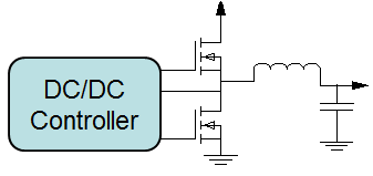
This feeling may be familiar to experienced power designers who have been using controllers with external field-effect transistors (FETs) for years, or really to any power engineer who has typically used only a DC/DC controller or DC/DC converter. It’s easy to get stuck in our ways, but stepping back and making sure that you know the big picture is good to do from time to time. In this post, I will delve into the considerations when choosing between designing with DC/DC step-down converters with integrated FETs (Figure 1) vs. DC/DC step-down controllers with external FETs (Figure 2).


Figure 1: DC/DC converter simplified diagram


Figure 2: DC/DC controller simplified diagram

Designing with a controller

Designing with controllers offers many benefits, including flexibility, thermal spacing, higher output currents and voltages, and lower cost.

Controllers with external FETs also have a few technical advantages over converters. Since the FETs are not integrated into the same package, controllers have better thermal spacing – a key trait for particularly heat-constrained designs. Controllers can also typically supply higher output voltages and currents than converters, enabling higher-power applications that converters might struggle with.

Since you will have flexibility in your FET selection, electing to go with controllers in many cases will help save on bill-of-materials (BOM) cost. Controllers are typically a more cost-effective option than converters, and when you combine that cost savings with the savings from lower-cost external FETs, the savings really add up. Cost is a key factor for just about everyone, so being able to save money on your power design is a huge plus.

Designing with a converter

Designing with a converter also offers many benefits, such as ease of use, smaller size and fewer components.

Choosing to use a converter may be an easier solution if you don’t want to spend a lot of time on the external circuitry part of the design (such as power FETs). Converters offer a more plug-and-play type experience, which is perfect if you have limited time or resources.

Improvements in integrated FET technology over the past several years have shrunk converter sizes. Designing with a converter will save you more board space compared to a controller. If your design is extremely space-constrained, a converter may be your best friend.

Integrated FETs simplify the design process by reducing the amount of external components and making layout easier. An easier layout will help accelerate time to market. There are also many applications where a board may contain hundreds, if not thousands, of components. Having an integrated solution option that will lower the component count could be reason enough to select a converter.

Conclusion

You can use converters or controllers in a wide range of applications, from enterprise servers and communication base stations to automotive and industrial applications. Now that you’ve read this refresher on the trade-offs, you should be better equipped to make the best selection for your design. No matter which route you decide to go, both TI’s DC/DC step-down converters with integrated FETs and TI’s DC/DC step-down controllers with external FETs make excellent options for point-of-load applications.

Additional resource


When and how to supply an external bias for buck controllers – part 1

$
0
0

In multi-rail systems system designers often have to make the choice of where to tap into for the input rail for the buck controllers. Often it is from 12V or 24V rails, however in some cases it’s from 5V or 3.3V rails. I will be discussing the need to supplying external bias and its benefits in the first part of this 3 part series.

Well, it comes down to the metal-oxide semiconductor field-effect transistor (MOSFET) curves and operating the MOSFETs in their sweet spots. It also depends on the input voltage. Most controllers are designed for use in a 5V or 12V rail, yet in many cases system designers use the same controllers in lower voltage rails.

If you look at the data sheets of those controllers, the VIN range checks out OK, but are you really getting the best performance or highest efficiency possible when operating at 3.3V?

Let’s use TI’s LM27403 as an example. Figure 1 shows the applicable info from the data sheet.

Figure 1: LM27403 VIN range

The minimum VIN is 3V, so it passes the sanity check for use with a 3.3V rail. Now, let’s look at the block diagram for the LM27403, shown in Figure 2.

 Figure 2: LM27403 block diagram

VDD in Figure 2 powers both the low- and high-side drivers. The supply for the low-side driver is VDD and the supply for the high-side driver is CBOOT, also known as VDD-Dboot. This means that the low-side FET will see 3.3V for the gate drive and the high-side FET will see 3.3V minus the boot diode drop.

You’ll usually want to use controllers when your output-current needs are higher than 5A. Take a 15A application; Table 1 lists a few random FET choices.

Table 1: Some FET choices for a 15A design

Referring to Table 1 and Figure 3 you can see that the ID max and Rdson spec columns in the data sheet can be misleading when it comes to operating at 3.3V. Factoring in a 10% tolerance, examine the FET curves (in Figure 3) for 3V and the drain current in the Id at Vgs=3V column in Table 1. This is the significant parameter that tells you whether a FET can natively support operation at VIN = 3.3V. For example, the NTMFS4834N will not support a 15A application even though it has a low Rdson number (see the ID capability at Vgs = 3V in Figure 3). This same FET would be OK if you were supplying 5V to the VDD pin of the LM27403. But using FETs that are not designed for a 3.3V application will affect three things:

  • The FET won’t support the current, and the high Vds drop will cause high power dissipation or even damage the device.
  • Efficiency will be lower than expected due to the sharp increase in Rdson at 3Vgs.
  • If the controller uses Rdson for sensing the current limit, the current limit may not function correctly.

Good choice for a 3.3V input voltage/15A design                 Bad choice for a 3.3V input voltage/15A design

Figure 3: FET curves showing ID versus VDS for different gate voltages

Table 1 indicates that all of the FETs would be fine to use at Vgs = 5V.

Talking about MOSFET data sheets, the CSD17304Q3 and CSD17309Q3 data sheets show my favorite format depicting curves down to lower Vgs levels. Figure 4 shows the curves down to Vgs levels of 2.5V. Kudos to the applications team that did this.

Figure 4: FET curve from the CSD17309Q3 data sheet

How do you accomplish that practically for a 3.3V rail? This leads me to the question I asked at the beginning of this post; when to use an external bias for controllers.

In some cases external bias is used as an efficiency improvement measure. In other cases external bias makes it practical for the FET to support the current.  

Figures 5 and 6 shows the efficiency improvements for different configurations of VDD with different FETs.

How much current should the bias regulator be capable of supplying? It should be capable of providing the non-switching quiescent current plus the average gate-drive currents (Ibias). You can calculate this using Equation 1:

(Qg control FET + Qg synchronous FET) * Fsw                      (1)

Using the CSD87350Q5D as an example, Ibias = 30nc * 250kHz = 7.5mA.

Figure 5: Efficiency curves for the LM27403 and BSC032NE2LS/BSC010NE2LS, with internal and external bias


Figure 6: Efficiency curves for the LM27403 and NTMFS4834, with internal and external bias

Figure 7 shows the impact of DC bias on the switching waveform, with dc bias the rise times are fast.

Figure 7: Switching waveforms with and without DC bias

So as you can see, you have to pay careful attention to FET selection in controller designs that run off of a 3.3V rail. By pairing the right FET, you can get a trouble-free design performing at its best; by using a device that flexibly applies external bias, you can optimize your design for cost and highest efficiency.

In the next installment of this series, I’ll discuss these two topics:

  • Can you apply an external bias voltage to any controller VDD pin or VIN pin?
  • If you don’t have a 5V bias rail available in your system, can you generate a 5V bias rail from the DC/DC converter by using a charge pump? 


When and how to supply an external bias for buck controllers – part 2

$
0
0

In part 1 of this series, I discussed the need for external bias and under what conditions you need to consider it. In this installment, I will look at whether you can apply external bias to any controller.

As a rule of thumb, you cannot apply external bias to controllers that have a current limit for the control field-effect transistor (FET) (also known as the high-side FET). It boils down to how the current limit is implemented.

Let’s look at a couple of examples. The first device is the LM3495, an emulated peak-current-mode buck controller. On first glance, it seems feasible that you can apply external bias on the VIN pin.

Reading through the data sheet, however, there is a section called High-Side Current Limit. A comparator monitors the voltage across the high-side FET when it is on. If the drain-to-source voltage of the high-side FET exceeds 500mV while the FET is on, the LM3495 will immediately enter hiccup mode. A 200ns blanking period after the high-side FET turns on prevents switching transient voltages from tripping the high-side current limit without cause.

Now, how is this voltage across the high-side FET actually monitored? The comparator has two inputs. The first input is the SW pin and the second input is the VIN pin. The assumption is that the drain of the high-side FET and VIN pin are always at one potential.

This configuration saves a pin, but it makes the external bias problematic. Let’s say that you apply 5V as the external bias to the VIN pin. The input voltage is 3.3V, applied to the drain of the high-side FET. This causes a 1.7V difference across the comparator looking for 500mV, so the controller enters hiccup mode.

The next device example is the LM27403. Looking through the data sheet, there is no current sensing for the high-side FET. Thus, you can use this device for supplying external bias to the VDD pin in low VIN applications.

How did I know to apply the external bias to the VDD pin? Let’s look at the block diagram of the device shown in Figure 1. Take note of the supply voltage shown for the low-side FET drive circuit; in this case, it’s VDD. If you look at the application circuit in Figure 2 you’ll see where CBOOT is connected through the diode. For the LM27403, it is also VDD. Thus, you can determine that VDD is the right pin with which to apply the external bias.

Figure 1: Block diagram showing VDD


Figure 2: Application circuit showing VDD

Now the question is how to determine what value of voltage is OK to apply at the VDD pin. For this, you need to refer to the absolute maximum ratings of the VDD pin and make sure that the external bias applied does not violate this rating. Looking at the LM2403 data sheet, the absolute maximum for VDD is 6V and the recommended operating maximum is 5.5V.

5V is a common rail on boards and would serve as an appropriate bias voltage. The bias voltage needs to be a regulated voltage in order to not violate the absolute maximum ratings of the VDD pin.

In part 3 of this series, I will explore ways to generate your own external bias voltage (in the event that 5V rails are not available) by using charge-pump schemes from the very supply to which you need to supply the external bias.


Power a RS-485 transceiver with a high efficiency flyback converter

$
0
0

RS-485 is a standard defining the electrical characteristics of drivers and receivers for use in serial communication systems. It defines not only a single device-to-device interface, but also a communications bus that can form simple networks of multiple devices.

RS-485 runs on twisted-pair cable, and the voltage differential of the two lines defines the logic, as shown in Figure 1. Because of its simplicity, low cost and good noise immunity, RS-485 is widely used in factory automation, building automation and metering applications.

Figure 1: RS-485 network structure

The power supply of an RS-485 device is normally single 5V or 3.3V, and the current consumption is below 200mA. Taking the TI SN65HVD888 as an example, the suggested power-supply voltage is between 4.5V to 5.5V. Many RS-485 networks use isolated bus nodes to prevent the creation of unintended ground loops and their disruptive impact on signal integrity. An isolated bus node typically includes a digital isolator between the bus transceiver and the microcontroller. It also requires an isolated converter to power the SN65HVD888.

The 5V Output, 4,000V Isolated Power Supply Reference Design for RS-485 Applications introduces a high-efficiency, cost-effective circuit for the 5V isolated power requirement. With a 5V to 20V input-voltage range and at least 200mA of output current capability, you can easily implement the circuit in your system board.

The reference design is based on flyback topology using the TPS61046, as shown in Figure 2. The TPS61046 is a 28V output, 900mA switch current boost converter. You can replace it with the TLV61046A small-outline transistor (SOT) package if you prefer.

The transformer supports up to a 4,000V isolation voltage. It has an auxiliary winding to sense the output voltage on the primary side. Ideally, the voltage in the VSEN node is almost the same as in the 5V node; thus, you can regulate the output voltage by regulating the VSEN. The method is called “primary-side regulation.” Compared to the method that senses the voltage directly in the secondary side, the benefit of primary-side regulation is that the optocoupler and reference voltage integrated circuit (IC) are not required, which greatly reduces the solution cost.

Figure 2: A schematic of a primary-side regulation flyback

However, the leakage inductance of a nonideal transformer can cause the output voltage to go out of regulation when the load changes. This leakage inductance is inevitable for a real transformer. Methods to optimize the leakage inductance, such as a better magnetic core or special winding arrangement, will result in increased transformer cost.

The leakage inductance also causes extra current flowing into the VSEN node. As the TPS61046 always regulates the VSEN to the set voltage, the voltage at the 5V node would be out of the 4.5V to 5.5V range required by the transceiver. To solve this problem, introducing a dummy load in the VSEN and 5V nodes absorbs the extra current caused by the leakage inductance. This dummy load is traditionally a fixed-value resistor. However, as the energy of the leakage inductance changes with the real load, the required dummy load should be small at a small real-load condition and large at a large-load condition. But you cannot easily optimize the fixed dummy load to make sure that the output voltage stays within 4.5V to 5.5V if the load varies from 0 to 200mA. Furthermore, the fixed dummy load will greatly reduce the efficiency of the converter in light-load conditions.

The TPS61046 integrates a power-save-mode feature that reduces the switching frequency during light-load conditions to improve efficiency. In heavy-load conditions, the device operates with a constant switching frequency. Using the power-save-mode feature adds a special circuit comprising R4, R5, Q1 and D5 (as shown in Figure 2) to solve to the load regulation problem.

The circuit adjusts the dummy load automatically according to the real load conditions. When the real load is small, the switching frequency and on-time of Q1 are small, so the dummy current is also small. When the real load increases, the switching frequency and on-time of Q1 increase, so the dummy current also increases. This self-adjustable dummy load helps improve load regulation and efficiency. Figures 3 and 4 show the test data in the evaluation board of the reference design.

Figure 3: Load regulation at different input voltages

Figure 4: Efficiency at different input voltages

Beyond the TPS61046, you can use almost all boost converters to build an isolated flyback converter. You just need to select a suitable boost converter based on the input voltage, output voltage and output current, and solution cost.

Additional resources


Power Tips: How to protect a USB Type-C™ controller from legacy adapters

$
0
0

In the last couple of years, more and more portal devices such as notebooks and smartphones have employed USB Type-C™ as the interface port. The USB Type-C connector is a totally new USB connector. It has a set of great profile, power rating and data transmission speed improvements. But the most important change about this charging protocol is that USB Type-C introduces a new pin, the configuration channel (CC) pin, to negotiate between different devices.

Legacy adapters use D+/D- lines to perform a handshake between two devices. The most common legacy adapters, as shown in Figure 1, usually have a Type A port as output so that different cables can be match with different phones; for example, an A-uB cable for Android phones, an A-lighting cable for iPhones, etc. USB Type-C also has an A-C cable so that it can be charged by legacy adapters.

Figure 1: A legacy USB adapter

To give users the best usage experience, some USB Type-C product manufacturers have designed their USB Type-C products to support both the new USB Type-C charging protocols via CC as well as existing charging protocols. Employing D+/D- in current USB products, some of the charging protocols cannot be used for USB Type-C connectors (see Section 4.8 of the USB Type-C Cable and Connector Specification, Revision 1.2).

There lies the problem. A USB Type-C connector has an A-C cable to be compatible with legacy adapters and there is an internal pull-up resistor (Rp) inside the USB Type-C plug (see Section 3.5 of the USB Type-C specification) to enable the detection of a USB Type-C device. Once there is a DC voltage existing at VBUS and the USB Type-C plug is inserted to the USB Type-C device, VBUS will pull up the voltage level of the CC pin to notify the USB Type-C controller, as shown in Figure 2.

Figure 2: Legacy adapter to a USB Type-C product connection

Even the fast –charging protocols such as QC are not compatible in a USB Type-C connector, the irregular USB Type-C products, as mentioned above, are still going to support these high voltage protocols. In this case, the VBUS may increase to 9V or 12V after a successful handshake with a legacy adapter via D+/D- lines. This high voltage will be applied to the CC pin of the USB Type-C controller via Rp. Unfortunately, the most common USB Type-C controllers cannot handle such high voltage, because it is out of the USB Type-C specification. To prevent the USB Type-C controller from being damaged in  the case of being tied to VBUS via Rprequires a compliant USB Type-C device.

One simple way to protect the USB Type-C controller is to add a Zener diode between the CC pin of the USB Type-C controller and ground. This Zener diode can clamp the CC line’s voltage within a safe range. But I need to highlight two things:

  • The clamping voltage of the Zener diode should be higher than the normal voltage of the CC pin and lower than the maximum rating voltage. But because a Zener diode’s breakdown voltage always varies with its own current (in this case, proportional to the VBUS voltage) and temperature, selecting a proper Zener diode won’t be easy.
  • The current flowing from VBUS to ground via the Zener diode brings additional losses. This current may be up to several milliamps in the worst case (given that VBUS may be up to 20V and Rp is lower than 10KOhm ).

Another way to protect the USB Type-C controller is to use a blocking field-effect transistor (FET) , labeled as QB in Figure 3,QB to isolate the USB Type-C controller from VBUS. The QB is inserted between the USB Type-C receptacle and USB Type-C controller. It can be off when an overvoltage event occurs at the CC pin of the USB Type-C receptacle so that the USB Power Delivery controller does not see such a high voltage. However, this will bring an additional path consisting of a pull-down resistor (RD in figure 3) and its control FET (QD in figure 3). QD will be ON to perform the RD on CC pin in the event of a dead battery. The additional logic circuit for QD may also sacrifice some board space.

A good choice is to adopt a USB Type-C port protection integrated circuit (IC) such as the TPD2S300, which integrates all of the necessary functions for a USB Type-C device. This IC requires no additional protection and logic circuitry. Electrostatic discharge (ESD) protection is integrated as well. Figure 3 shows a typical circuit using the TPD2S300.

Figure 3: TPD2S300 circuit for the CC pin

To protect the USB Type-C devices, such as power banks or smartphones, from irregular adapters or chargers on the market, additional protection for the USB Type-C port is necessary with Zener diodes, blocking FETs or protection ICs.

When and how to supply an external bias for buck controllers – part 3

$
0
0

In part 1 of this series, I discussed the need for an external bias and under what conditions you need to consider one. In part 2, I discussed whether you can apply an external bias to any controller. In this third and final installment, I will go over a circuit that you can use to generate an external bias for any controller. This may prove useful in cases where a 5V bias rail is not available for providing the external bias.

Looking at Figure 1, the shaded region is the external circuit for the bias. Ric represents the current drawn by the integrated circuit (IC).

Figure 1: External bias circuit shown in the shaded box

You must make sure that the external bias circuit can provide the current, since it depends on the operating frequency, selected field-effect transistors (FETs), etc.

Iic = (Qg(Q1) + Qg(Q2))*1e-09*Fsw*1e03                              (1)

Let’s plug in some numbers and use the example of a device running at two different frequencies and using the TI CSD87381P NexFET™ power block. These are the simulation conditions:

  • Qg(Q1) = 3.9nC.
  • Qg(Q2) = 6.2nC.
  • Iic = 12mA at 1,200kHz.
  • Iic = 5mA at 500kHz.

Once you figure out Iic, you can calculate Ric for the simulations by Vext_bias/Iic.

Run the simulations with the calculated Ric and make sure that Vext_bias does not exceed the absolute maximum of the VDD pin, or the pin of the IC where you need to apply the external bias. In some cases, you may need a Zener diode or additional loading resistors.

Figures 2 and 3 show the circuit waveforms. You can see that I generated close to 5V for the external bias. As the efficiency curves in part 1 of this series illustrated, this approach helps increase efficency or enables circuits to support higher currents, whatever the case may be.

Figure 2: Waveforms at Fsw = 1,200kHz at Iic = 12mA


Figure 3: Waveforms at Fsw = 500kHz at Iic = 5mA

There are many charge-pump schemes possible with various variants and I have demonstrated a simple method to implement an external bias. One point to note is the variation of the 3.3V rail. If the 3.3V rail has a wide tolerance, I recommend placing a Zener diode to clamp the voltage applied to the VDD pin in case of overshoot on the input voltage rail.

Thank you for reading this series of blogs. I hope you learned when and how to supply an external bias for buck controllers. Feel free to post a comment if you have any questions.


Power solution selection for a Xilinx Ultrascale/Ultrascale + FPGA made easy

$
0
0

Given their high performance and integration capabilities, several data center and industrial applications use Xilinx® Ultrascale™ and Ultrascale+ field-programmable gate arrays (FPGAs), including enterprise switches, server FPGA accelerator cards, test and measurement, and space and defense.

Knowing the Xilinx FPGA power specifications for a particular Ultrascale+ FPGA family – Zynq multiprocessor system-on-chip (MPSoC), Virtex, Kintex – requires downloading and using the Xilinx Power Estimator (XPE), as shown in Figure 1.

Figure 1: XPE tool header

Once on the XPE site, you’ll select the settings that correspond to your device family (Zynq Ultrascale+, for example), device part number (such as the XCZU9EG), speed grade, temperature grade and environment (including board size and layers). You’ll then complete the power profile by selecting the clock, logic, input/output (I/O), RAM, digital signal processor (DSP) and transceiver options.

TI has done the pre-work and created a spreadsheet with all Xilinx Ultrascale+ Family variants, their corresponding part numbers, rail names, loading options (choices of clock/logic/I/O, RAM, DSP and transceiver) and voltage and current specifications, as shown in Figure 2.

Figure 2: Xilinx Ultrascale+ device number power specs

These detailed power specifications for every Xilinx Ultrascale+ FPGA family, device number and loading type (low/medium/high) will soon be represented in TI’s Xilinx FPGA power selection portal, as shown in Figure 3. Xilinx Ultrascale FPGAs and TI’s power solutions are already represented in this portal.
 
Figure 3: TI’s Xilinx FPGA power solution selection portal
 
As you can see in Figure 3, depending on the loading (low, medium, high), the power solution may vary to optimize the performance/efficiency/density/cost of the specific design.
 
Based on TI’s summary of the XPE power requirements of Ultrascale+ FPGA families and the solution recommendation on TI’s Xilinx power solution selection portal, you may be able to get a head start on your board design with a corresponding reference design in the TI Designs reference designs library. For example, for the Virtex Ultrascale XCVU065 medium-loading VCCINT rail 120A requirement, TI’s FPGA power solution selection portal recommends the TPS53647DCAP+™ control mode buck controller with PMBus.
 
Figure 4 shows a 1V/120A four-phase buck from the High Efficiency, Power Density 1V/120A/30A/30A (4+1+1) with PMBus Reference Design  that you can use for this requirement.


A noteworthy feature of TI’s FPGA power solution selection portal is that hovering over the TI device number also gives you a quick overview of the specific WEBENCH® Designer results for that Xilinx FPGA (as shown in Figure 5), making it easy for you to make a first-level decision.
Figure 5: Quick look at the Xilinx Virtex Ultrascale XCVU065 12V input, VCCINT rail, high-loading (200A) WEBENCH Designer results
 
You can find and download the various Xilinx FPGA designs on the TI reference designs selection page. Type Ultrascale or Ultrascale+ in the Keyword box, get the results, and then filter for your particular FPGA or type of solution (power-management integrated circuit [PMIC], discrete buck converter/controller, multiphase buck or module), as shown in Figure 6.

Figure 6: Finding Xilinx Ultrascale/Ultrascale+ FPGA reference designs on the TI reference designs selection page
 
You can also click the Search power designs by parameters tab and check the FPGA box. This will give you all of the available FPGA reference designs in tabular form, as shown in Figure 7, which you can filter for the Xilinx Ultrascale/Ultrascale+ reference design that you need.
 
Figure 7: Finding Xilinx Ultrascale/Ultrascale+ FPGA reference designs on the TI reference designs selection pageby using the FPGA filter
If you are designing with Xilinx Ultrascale/Ultrascale+ FPGAs and don’t know where to start, TI has made it easy to select the power solution, find the optimal reference design from the TI Designs reference design library, and get ahead of the competition with our easy-to-use power selection and design tools.

Design a 3A power supply smaller than a 1608-size resistor

$
0
0

Is it easy for you to physically see all of your integrated circuits (ICs) on your printed circuit boards (PCBs), or do you need a magnifying glass to see the small bits of black plastic sprinkled in among the larger resistors, capacitors and inductors? Over the previous few years, passive components – especially power inductors – have gotten smaller and smaller. 1608-sized inductors (1.6mm by 0.8mm) are now common, with rumors that 1005 sizes (1mm by 0.5mm) are coming soon.

These 0603 (60mils by 30mils) and 0402 (40mils by 20mils) sizes often made the ICs, at 2mm by 2mm or 3mm by 3mm, look large in comparison. Not anymore. For those of you designing the latest smartphones, personal electronic accessories and solid state drives (SSDs), the tables have turned. New solutions are available that are 80% smaller.

A 3A step-down (buck) converter (TI’s TPS62088) is achievable in a mere 1.2mm by 0.8mm wafer chip-scale package (WCSP), which is a type of ball-grid array (BGA) package. That’s less than 1mm2 of board space for the DC/DC IC. If that’s too small for you, there’s also a 3A step-down converter (the TPS62823) in a larger and more traditional quad flat no-lead (QFN) package, measuring just 2mm by 1.5mm. Both of these power-supply ICs are once again smaller than the power inductors surrounding them, as shown in Figures 1 and 2.

Figure 1: A 3A DC/DC is smaller than a 1608-size resistor


Figure 2: A 3A DC/DC is smaller than a 2016-size inductor

Is this still too big, you say? Although the above solutions are truly small for 3A devices, they offer much more power than what the smallest systems need, such as wearables. For these, 1A of output current is more than enough for any rail in the system. If you just need an amp or less, the TPS62801 shown in Figure 3 checks in at a mere 1.05mm by 0.7mm – not quite as small as a 1005-size component, but smaller than any 1A power supply on the market.


Figure 3: A 1A DC/DC is almost as small as a 1005-size capacitor

So what’s the secret behind these smallest DC/DCs? Quite simply, a high switching frequency and a stellar silicon process. The three DC/DCs described here switch between 2.4MHz and 4MHz, which enables you to use either 0.24µH or 0.47µH inductors. With fewer physical turns of wire required on the inductor’s core to generate this very low inductance, physics says that it is easier to make the inductor smaller.

Of course, I can’t go into details as to what makes the power-optimized process so innovative; I’ll just let the results speak for themselves. The internal power transistors have both very low resistance and very low gate charge to produce high efficiencies at high currents, while switching at very high frequencies. Furthermore, the low quiescent current (IQ) of 5µA or less sustains the high efficiency down to very light loads.

Figure 4 shows that the efficiency for a common 5VIN to 3.3VOUT converter is still very high at 93% even at its full 3A load, with a peak of 95% at a 1A load. Near 90% efficiency is maintained at a very light 100µA load. There is no efficiency degradation, even while operating at 4MHz. Such high efficiency results in longer battery life for portable systems and a lower temperature rise for both portable and stationary systems.


Figure 4: TPS62088 efficiency is over 90% across the entire load range

In your system, where do you need the smallest DC/DCs?

Additional resources

How to Select a MOSFET – Part 1

$
0
0

In complicated power designs, metal-oxide semiconductor field-effect transistor (MOSFET) selection has a tendency to be somewhat of an afterthought. After all, it’s just a three-pin device. How complicated can it be, right? But as anyone who enjoys raw oysters will (try to) tell you, appearances can be deceiving; trying to select the correct MOSFET or “FET” can be a task more complicated than you might think.

In this 7-part blog series, I’ll analyze a variety of typical FET applications, from power supply to motor control, and address the various concerns and trade-offs that dictate the FET selection process. Hopefully, whether you’re a FET novice or an advanced apps engineer, you will find this series insightful the next time you have to decide on a MOSFET best suited for your system (and budget).

How to Cross-Reference a FET

A common and simple MOSFET selection process is the exercise of finding a cross-reference for a FET where the end application is generally unknown. Often times a purchasing representative will provide the engineer an exhaustive list of FETs that their client is using, with no indication as to how those devices will be used. It could even be that some FETs will be used on several different boards in multiple configurations, and they are just looking to see if you have something similar in performance to offer.

Every month, I must get dozens of requests from our field sales folks to provide TI “crosses” to our competitors’ FETs; while we try to maintain our internal cross-reference database, keeping track of every FET vendor’s entire MOSFET portfolio is a somewhat futile task. As such, the need to make crosses manually isn’t going away anytime soon. So let’s break down the process into three easy steps:

  1. Match the package. This may or may not be necessary, depending on whether the end application board requires footprint compatibility. If it does not, that probably opens the door to many more options, but in general, it’s a good practice to suggest something of equal or lesser footprint size. It’s important to remember that different FET vendors have different names for different packages, especially when it comes to power quad flat no-lead (PQFN)-type devices. You can always check the mechanical drawing, which is typically provided in the back of the data sheet, to confirm the footprint compatibility of two different vendors’ packages (see Figure 1).

Figure 1: A TI small-outline no-lead (SON) 5mm-by-6mm package’s recommended printed circuit board (PCB) footprint (in green), overlaid on two competitors’ differently named 5mm-by-6mm surface-mount devices (shaded and white, respectively) shows that they are footprint-compatible

2. Match the breakdown voltage. FETs are designed to block a certain voltage, so the cross needs to have an equal or greater value breakdown voltage than the original. While selecting a FET with a higher breakdown is not technically a problem, the higher the breakdown voltage, the higher the resistance per unit area (RSP) of the silicon die, and thus the more expensive the device will have to be in order to achieve similar performance. Crossing a 60V FET for a 55V FET is probably no issue, but cross a 100V to 30V for the same performance and you will almost certainly see a major price gap.

3.Match the resistance. This is the most ambiguous step in the process. It is a common misconception that resistance is the most critical parameter in all FET applications, but given that you don’t know anything about the end application, resistance is all you have to go on. It’s still a better performance metric to cross against than anything else on the data sheet, like notoriously unreliable current ratings or gate charges, which may or may not be relevant depending on the design using the FET. When matching resistance, you can use typical or maximum values since the data sheet provides both (engineers often design to the maximum), but it is important to be consistent when doing so. A good rule of thumb is if two FETs are within ±20% resistance, they are a fairly close match.

    There are many more factors to consider before placing a FET on the board, but these three checks are a good starting point. TI’s MOSFET parametric search, shown in Figure 2, makes online selection within the three parameters quick and easy.

    Figure 2: TI’s parametric search makes it easy to select a MOSFET based on package, breakdown voltage and resistance, as well as other parameters

    A last point to note is that it’s always worth it to keep an eye on cost. An older silicon generation might require a lot more silicon to achieve similar performance, and while most vendors won’t advertise the silicon generation of every device in their portfolio, they will offer relative 1,000-unit pricing that should give some you indication. If you ever come across two different devices with the same package, voltage and similar resistance but much different pricing, it is very likely that the lower-priced device is a newer solution and often a better recommendation (though future installments of this series will investigate applications where this is not necessarily the case).  Questions?  Please feel free to leave a comment below.


    Design a second-stage filter for sensitive applications

    $
    0
    0

    Certain applications, such as test and measurement, are sensitive to voltage ripple and routinely require very low output voltage ripple. For example, 10µV/V of ripple ratio translates to 100dB of attenuation.

    Since it’s impractical to attain this level of attenuation using a buck regulator with a single-stage filter, a powerful design technique to reduce output voltage ripple is to use a second-stage inductor-capacitor (LC) filter, as shown in Figure 1. Proper configuration of the second-stage filter is essential for optimal performance.

    Figure 1: Buck with a second-stage LC filter

    In order to obtain a total of 100dB attenuation at the switching frequency, the first and second LC filter are designed to give an attenuation A1 (60dB) and A2 (40dB), respectively. For the first-stage filter, inductor L1 is designed to give a chosen ripple ratio based on the load current. In power modules, this L1 inductor is integrated inside the package.

    Equation 1 expresses the impedance of inductor L1 at the switching frequency as:

    Therefore, Equation 2 expresses the impedance of C1 at the switching frequency as:

    Equation 3 translates the required impedance XC1 to the value of capacitor C1:

    The impedance of the filter should be sufficiently low at the output so that it does not significantly affect the loop gain of the converter. Low output impedance also helps with better regulation over long trace lengths. This is particularly true in systems where you can’t maintain the load that the regulator is driving in close proximity to the regulator. As we can see from Figure 2, the ratio of first-stage capacitance (C1) to second-stage capacitance (C2) is critical to the impedance of the converter.

    To ensure low impedance and make sure that the filter doesn’t substantially affect the loop, I set the ratio of C1 to C2 as 1 to10.

    Figure 2: Closed output impedance with different filter designs

    Equation 4 expresses the impedance of C2 at the switching frequency:

    To get A2 attenuation, Equation 5 determines the impedance of L2 as:

    Equation 6 translates the required impedance XL1 to the value of capacitor L2:

    Many designers worry that the additional poles and phase delay of a second-stage filter will compromise loop stability. Actually, if you locate the additional double pole far away from the crossover frequency and keep it lower than the switching frequency, it won’t affect the bandwidth and phase margin of the converter.

    What you should pay more attention to is the Q of the second-stage filter. A high Q will lead to a low gain margin (as shown in Figure 3) and consequently unstable operation, such as an undamped response to a step input. So you must damp the Q of the second-stage filter, and there’s more than one way to do it.

    The easiest approach is to use electrolytic or polymer capacitors with equivalent series resistance (ESR). ESR is not a dependable factor, however, and would result in a reduction of ripple attenuation (an increase in output ripple). Another option is to add a resistor in parallel with the filter inductor as shown in Figure 4, which has the advantage of small size and low cost. The drawback is that it reduces the effectiveness of the filter at high frequencies because it reduces the effective impedance of the filter inductor.

    Figure 3: A high Q results in low phase margin


    Figure 4: Placing the resistor parallel to the inductor damps the Q

    Let’s use the LMZM23601 as an example, with VIN = 24V, VOUT = 5V, FSW = 750kHz and IOUT = 1A. The power module has a 10µH integrated inductor. So the impedance of L1 at the switching frequency is 47.1Ω. To get 60dB of attenuation for the first-stage filter, the impedance of C1 at the switching frequency should be 47mΩ, which is 4.5µF translated to capacitance. I chose 6.8µF to add some margin. Since the second-stage capacitor is set to 10x the first stage, the chosen value for C2 can be 68µF. The resulting impedance XC2 at the switching frequency is 3.1mΩ.

    To obtain the remaining 40dB of attenuation, the impedance XL2 should be 309mΩ, which is 65nH when translated to inductance. Since this inductor is going to see the output current, it is important to design for enough margin so that the inductor doesn’t derate with current. You could choose a 160nH inductor. In order to damp the Q, I added a 250m resistor parallel to inductor L2.

    Figure 5 shows the parameters I used in my example.

    Figure 5: The LMZM23601 with a second-stage filter


    Figure 6: Test output voltage ripple


    Figure 7: Bode plot with and without the second-stage filter

    As you can see from Figures 6 and 7, adding a second-stage filter is an effective way to reduce output voltage ripple. You can easily get 0.014% (0.7mV/5V) of output voltage ripple, which is good enough for most applications. At the same time, proper filter design won’t affect the stability of the converter. Learn more about TI DC/DC power modules.

    Batteries and the changing landscape of medical monitoring

    $
    0
    0

    As healthcare coverage expands to cover emerging technologies, batteries shrink and interconnectivity improves, the medical field is close to a paradigm shift in treatment options. In the next decade, doctors may commonly monitor hundreds of patients using online tools, avoiding in-person medical checkups and allowing health care systems to cope with an increasing volume of patients.

    Following this trend, more and more medical and personal electronics companies are embracing wearables to improve patient outcomes and higher quality of service during both the in- and outpatient treatment stages. These companies are helping increase patients’ quality of service through a variety of innovations to medical equipment, but one of their main focuses is to modify designs so that all patient care equipment is capable of following a patient throughout their stay. Currently, significant resources are dedicated to moving a patient and exchanging monitoring equipment between different wards. Nurses have to prepare large equipment to receive a patient from other wards, and logistics must be coordinated to return equipment to their original locations after a patient transfer, all of which costs time and effort. Equipment with better mobility smooths the transition from the intensive care unit, to the general ward to a patient’s eventual release. By eliminating the need to coordinate between departments or even outside organizations the transition-of-care process becomes more convenient by allowing the equipment to stay with the patient.

    Portability is not a new idea, since most traditional medical equipment has batteries already (albeit extremely large ones). The size of these batteries has made it too challenging for most patients to be easily mobile. In an effort to resolve this problem, companies have taken a new approach, using basic sensors as the primary monitoring tools and delegating auxiliary functions through connections to medical networks. Offloading all processing, storage and other non-monitoring processes reduces the cost of and surface area of medical equipment, making medical devices less expensive, lighter and more versatile. By monitoring patient information like those shown in Figure 1, medical devices from cutting-edge wearables to traditional hospital equipment like bedside monitors, drug-infusion pumps and sensor-packed beds can help patients and their providers stay connected.

    Figure 1: Patient information that can be tracked and transmitted by wearable monitors

    Interconnectivity improves a multitude of routine medical processes, including documentation, asset tracking and patient care. Automated documentation prevents mistakes when recording vitals. Constantly connected equipment maximizes use and makes it possible for machines to facilitate or even completely accomplish routine medical procedures.

    Take for example the process of preventing bedsores on bedridden patient. Traditionally, a nurse has to remember to change and record the patient’s position every few hours to prevent pressure sores. But a connected hospital bed or a sensor worn by the patient can expedite this process, automatically tracking movement and alerting nurses when action is necessary. These devices would also create an accurate log of the patient’s different positions, giving doctors a useful resource if the patient reports any pain or change in status.

    Through small improvements like these, a revolution is brewing. Doctors are now doing more with less, but only as long as these devices remain on. For this exact reason, all-day battery life is essential for patient convenience and outcomes.

    Constant communication and other features like touch screens consume energy at levels that prevent disposable batteries from being a viable solution within this new monitoring space. These batteries would drain quickly by providing this power, adding a large cost to the operation of each device.  Meanwhile rechargeable lithium-ion batteries are powerful enough to resolve the power problem but they require much more consistent temperature and protection, and charging them correctly is a big concern. For medical applications that are small and susceptible to electrical noise linear chargers can be used for the charging task. Linear chargers are simple to design into any power block and can provide charge currents of up to 1.5A, with smaller solution sizes than their switching counterparts.

    TI’s smallest linear charger, the bq25100, has termination current control with precision down to 1mA, a leakage current of only 75nA (which is negligible compared to the self-discharge rate of the battery cell) and one of the lowest bill-of-materials (BOM) costs on the market. This makes the bq25100 ideal for simple applications that require less than 250mA of charge current or precise termination currents, such as wearable applications and patient monitors.

    If you need a more complex charger, the bq25120A is a great alternative. This charger comes with integrated I2C, push-button controls, a low-dropout regulator (LDO), a buck converter, and fast charging and power-path capabilities, while still being smaller than three grains of rice. It has the capability to power systems while simultaneously charging the battery, allowing for instant-on functionality. The push-button control facilitates interfacing with the microcontroller (MCU) over the rails or interrupts, allowing easy access to different modes of operation. Fast charging allows for a high amount of charge in a small period of time in exchange for some extra wear and tear on the battery.

    The inclusion of I2C communication control adds a whole world of customization to this device. For example, the I2C interface enables you to customize the charge profile through the MCU. You can configure the charge voltage, charge current, termination threshold, input current limit, safety timer limit and much more to meet a wide range of specifications. This customization results in light wearable solutions with small batteries to charge without having to sacrifice performance or customization. Customization also enables lower termination currents, which means you can charge batteries to higher capacities every cycle. See Figure 2.

    Figure 2: The benefits of a low termination current

    Figure 3 shows the use of either the bq25100 or bq25120A linear charger in a wearable electrocardiogram (ECG) patch. This ECG patch would enable someone who has had a recent heart procedure to constantly track their vitals without having embarrassing wires or machines connected to them. The miniaturization of devices like the bq25120A makes this design possible.

    Figure 3: ECG patch system diagram

    Batteries are becoming an integral part of medical technology because of the growing need for small solution size, which enables portability, longevity and continuous interconnectivity.  Using devices that constantly monitor the state of a patient’s health not only enhances patient care, but improves healthcare processes within a hospital or medical facility. Size-conscious linear charges like the bq25100 and bq25120A maximize the longevity of the battery, allowing something like an ECG patch to keep up with the patient’s health needs without the constant battery replacement that would interfere with monitoring.

    Of course, TI offers many more linear chargers than just the ones I’ve mentioned here, and we are continually developing more variations to keep up with the latest demands from the medical industry. This includes supporting the newest waves of patient monitoring systems that will help impact modern health care from the ICU to a patient’s home for the better by making patients more mobile and providers more efficient. The future is uncertain, but it does look bright.

    Additional resources:

    TurboTrans™ technology: one resistor dramatically improves transient performance and reduces solution size

    $
    0
    0

    Ever-evolving technology demands smaller, modular, performance-driven solutions. Power modules contribute to very small solution sizes and smaller board-space requirements, but can come at the cost of design flexibility. Many newer DC/DC regulators and power modules internalize loop compensation or feature operating architectures that do not require loop compensation, making them very easy to use. But in some cases, that could reduce your ability to fine-tune design performance.

    For example, as process technology advances, processors require tighter voltage accuracy and lower core voltages. Table 1 is a chart from a field-programmable gate array (FPGA) datasheet stating that the recommended operating conditions for the VCCINT rail are 1V, plus and minus 30mV. The manufacturer doesn’t recommend any voltage outside of this 3% range because the processor could behave unexpectedly outside this voltage window. Thus, you may have to increase the capacitance at the output of DC/DC converters to meet the 3% range during load changes.

    Symbol

    Min

    Typ

    Max

    Units

    FPGA logic

    VCCINT

    0.97

    1.00

    1.03

    V

    0.87

    0.90

    0.93

    V

    VCCBRAM

    0.97

    1.00

    1.03

    V

    0.87

    0.90

    1.03

    V

    Table 1: Recommended operating conditions for a field-programmable gate array (FPGA)

    While small capacitance increments are allowable, much larger amounts could negatively affect the module’s load transient response. To optimize transient response, designers typically add a feedforward capacitor (CFF) in parallel with the upper feedback resistor, as shown in Figure 1. In the frequency domain the addition of CFF creates a zero, which increases bandwidth and improves the transient response time.

    Figure 1: Feedback divider with feedforward capacitor CFF

    Unfortunately, while CFF creates a zero to help increase bandwidth, it also creates a subsequent pole as a product of CFF and the parallel combination of feedback resistors. This pole can negate the benefits brought about by the zero of the CFF. Since CFF adds a zero and a pole, which may not be too far apart in frequency, the choice and calculation of CFF becomes tricky. The right CFF value will help the situation, while a wrong CFF value will bring no improvement and will just be a useless addition to the bill of materials (BOM).

    TurboTrans™ technology, shown in Figure 2, improves the loop response by adding just one resistor (RTT). Adding an RTT resistor enables you to optimize the feedback loop easily using a resistor outside of the module. By adjusting the TurboTrans resistor, you can optimize the zero and midband gain (AVM) of the compensation stage as required. There are no side effects like that of a consequent CFF pole with the use of a RTT resistor.

    Figure 2: Power module with TurboTrans technology

    The RTT resistor is nothing but an additional series resistor in the Type II compensation scheme. This additional RTT resistor doesn’t require in-depth knowledge of loop compensation techniques because, like for any other power module, the data sheet will provide an equation to calculate the right value. Your calculation will simply depend on the amount of total output capacitance. The RTT will compensate for any additional capacitance at the output, and the load transient response will remain spectacular.

    Let’s use TI’s TPSM84824 to show how TurboTrans technology helps achieve a fast transient response. In order to meet the 3% range (recalling Table 1), the only thing you can do in the absence of TurboTrans technology is increase the output capacitance. As you can see in Figures4 and Table 2, capacitance increments have little effect on the voltage droop. That’s because with increasing output capacitance, the overall bandwidth of the regulator reduces considerably (as shown in Figure 3). This makes the loop slow and increases the time required to react to a load transient. Consequently, even with a large value of output capacitance, the power module still cannot maintain less than 30mV of voltage droop.

    Figure 3: Gain curve with different output capacitance


    Figure 4: Transient response with different output capacitance

    Output capacitance (µF)

    Crossover frequency (kHz)

    Voltage droop (mV)

    188

    41.0

    114.6

    288

    31.3

    103.2

    388

    26.0

    92.4

    488

    22.8

    86.4

    588

    20.5

    82.2

    Table 2: Voltage droop with different output capacitance

    The situation improves if you use the TurboTrans feature. By adjusting the TurboTrans resistor, you can easily get 17.4mV of voltage droop, as shown in Figure 5.

    Figure 5: Transient response with TurboTrans technology

    As the experimental results show, TurboTrans technology enables you to considerably improve the performance of your power module. Depending on the application, this feature can also help reduce the overall capacitance at the output, thus reducing system cost and size.


    Additional resources


    How to Select a MOSFET – Part 2

    $
    0
    0

    In part one of this series, we looked at how to suggest an appropriate cross reference for a FET when the end application is unknown. In this blog and those upcoming entries in this series, we’ll start to look at what specific considerations to take into account for a certain end application, starting with FETs that will be used in the end application to drive a motor.  Motor control is a large (and rapidly growing) market for 30V-100V discrete MOSFETs, particularly for a number of topologies that drive DC motors. Here, I’ll focus on selecting the correct FETs to drive brushed, brushless and stepper motors. While there are very few hard rules and a potentially infinite number of different approaches, I hope that this post will give you some idea where to start based on your end application.

    The first and probably easiest choice to make is what breakdown voltage you require. Because motor control tends to be lower frequency and therefore causes lower ringing compared to power-supply applications, there is a tendency to be a bit more aggressive with the margin between the input supply rail and the breakdown of the FET (often at the expense of using a snubber) in order to obtain a lower-resistance FET. But in general, a 40% buffer between BVDSS and the maximum input voltage, VIN, is not a bad rule – give or take 10% depending on how much ringing you anticipate and how much you are willing to dampen said ringing with external passive components.

    Selecting a package type is perhaps the most critical decision, and depends entirely on the design’s power-density requirements (see Figure 1). Below 2A, FETs are most often (but not always) absorbed into the driver integrated circuit (IC). For stepper motors and low-current brushed and brushless applications below 10A, small-form-factor PQFN-type devices (SON 2mm by 2mm, SON 3.3mm by 3.3mm) offer the best power density. If you’re prioritizing low cost over higher power density, older SOIC-type packages might get the job done, but will inevitably take up more printed circuit board (PCB) space.

    Figure 1: Various packaging options for driving different motor currents (packages not shown to scale)

    The 10A-30A space that small battery-powered tools and home appliances occupy is the sweet spot for 5mm-by-6mm QFNs. Above that, higher-current power and gardening tools tend to either parallel multiple FETs, or they implement bigger packaged devices like D2PAK or through-hole packages like the TO-220. These packages can house more silicon, enabling lower resistance, higher current capability and better thermal performance. Mounting through-hole packages on large heat sinks also dissipates even more power.

    The question of how much power a device can dissipate depends just as much on the thermal environment of the end application as it does on the package of the FET. While surface-mount devices generally dissipate most heat through the PCB, you can attach other packages like the aforementioned TO-220 or TI’s DualCool™ power block devices (Figure 2 below) to a heat sink in order to pull heat away from the board and increase the maximum power that the FET can dissipate.

    The last thing to look at is what resistance you should be targeting. In some ways, selecting a FET to drive a motor is simpler than selecting a FET for a power supply because lower switching frequencies dictate that conduction losses dominate thermal performance. I don’t mean to imply that you can entirely neglect switching losses in PLOSS estimations. On the contrary, I have seen worst-case scenarios where switching losses can represent up to 30% of the total PLOSS in a system. But these losses are still secondary to conduction losses and therefore shouldn’t be your first consideration. Power tools designed around ultra-high stall currents generally tend to push the FETs to their maximum thermal capability, so the lowest-resistance devices in a given package are a good place to start.

    Lastly, I would like to revisit the power block devices mentioned prior. The 40V CSD88584Q5DC and 60V CSD88599Q5DC are two vertically integrated half-bridge solutions housed in a single 5mm-by-6mm QFN DualCool package (see Figure 2). Doubling down on the low resistance per footprint offered by traditional discrete 5mm-by-6mm devices while offering an exposed metal top for the application of a heat sink, these devices are uniquely suited to handle higher currents (40A and more) in space-constrained applications.

    Figure 2: Stacked die power block mechanical breakdown

    Before resorting to a bulkier TO package for your design, it might be worth it to run the numbers on one of these power blocks to see if you can save some serious space on PCB footprint and heat-sink size. Questions?  Please feel free to leave a comment below.

    Additional resources

    Powering FPGAs - What to consider with Xilinx UltraScale+ FPGAs

    $
    0
    0

    Have you ever driven across a one-lane bridge or been in traffic with cars on either side? In such instances, there may only be a few feet of margin of error when steering. If your car was wider, the margin of error would decrease and steering would require more precision. The inverse is also true; the margin of error would increase if the car was narrower.

    The rails on Xilinx UltraScale+ devices aren’t much different; there is an operating range in which the power supply’s output must remain, and the supply itself has a given “width” based on a deviation from the target output voltage. So how do you decrease this deviation from the target output voltage? The first thing to do is to identify factors that can impact output voltage accuracy. In this post, I will discuss the errors introduced by reference voltage accuracy and feedback resistor tolerance, and methods that reduce or eliminate these errors when choosing DC/DC buck converters for your UltraScale+ application.

    To understand why this deviation from the target voltage is so important, let’s consider a common rail rating for UltraScale+ devices for a particular speed grade shown in Table 1. Please note that this rating could differ depending on your particular device’s speed grade. You should always consult the data sheet for your particular device.

    Min

    Typ

    Max

    Unit

    0.825

    0.850

    0.876

    V

    Table 1: Common voltage ratings for VCCINT, VCCINT_IO, and VCCBRAM for Kintex, Virtex and Zync UltraScale+ devices

    Now, let’s visualize what those numbers mean in terms of operating range. Figure 1 shows the full range of AC ripple allowed by the power supply’s output voltage.

    Figure 1: Power supply’s AC ripple output voltage range

    According to Figure 1, there is approximately 50mV that the power supply’s output can deviate from the target voltage of 0.85V, or ±25mV (3% of the target voltage) for AC ripple. Actual load current and transient specifications, including transient step size and slew rate, would depend on resource usage of UltraScale+ devices, but you can estimate them using the Xilinx Power Estimator (XPE) tool.

    Figure 2 shows a simplified feedback divider circuit for a DC/DC buck converter, highlighting those components that can decrease the output voltage accuracy. This is a generalization of the actual circuit; certain devices may have different naming conventions and use different pins altogether. The output voltage is divided down and sensed at the input of an error amplifier, where it is compared to a reference voltage (VREF). The output of the error amplifier (a magnitude of the difference between the two inputs) is used to set the pulse-width modulation (PWM) logic accordingly, in order to keep your output voltage to the desired target voltage. Altering the divider ratio or the value of VREF impacts the output voltage, so what happens when you factor in the reference voltage accuracy and feedback resistor tolerance? In order to answer this question, let’s work through an example based on a typical design.

    Figure 2: A simplified resistive feedback divider circuit (left); the same circuit with components that can decrease output voltage accuracy highlighted (right)

    For this example, I’ll use resistors with a 1% tolerance rating for the feedback divider. The reference voltage will depend on the device, but let’s say that it that has a rated reference voltage of 0.6V with ±0.5% accuracy, as shown in Table 2. You can find this reference value and any deviation over temperature in a device’s data sheet.

    Parameter

    Min

    Typ

    Max

    Unit

    VREF

    0.597

    0.600

    0.603

    V

    Table 2: Common reference voltage rating for TJ = 25°C

    You now can calculate the error introduced by using:

    • The resistor tolerance of the top resistor, TR_TOP, and the bottom resistor, TR_BOT, since they are equal: TR_TOP = TR_BOT = TR.
    • The deviation in the reference voltage: ΔVREF.
    • The typical reference voltage: VREF.
    • The target output voltage: VOUT.

    Plugging these terms into Equation 1:


    Let’s revisit the initial graph showing the full range of AC ripple that the power supply’s output voltage allows, with the accuracy error just computed. Figure 3 shows three regions: The white region surrounding the target output voltage is the accuracy error for the previous example, and the two light-green regions are the remainder of allowable AC ripple. Originally this number was 50mV, or ±25mV. After you consider the accuracy error, the new value is approximately 32mV, or ±16mV. This is less than two-thirds the original operating range.

    Figure 3: Power supply AC ripple output voltage range for VREF = 0.6V and TR = 1%

    So what can you do to reduce this output voltage accuracy error? Higher-precision feedback resistors could certainly work, especially with a rated tolerance of 0.1%, for instance. But what if you could eliminate the error introduced by the resistor tolerance completely for this rail, or in some cases reduce the reference voltage error to negligible values?

    To eliminate the error introduced by the tolerance of the feedback resistors, you simply need to choose a device that has the option to adjust the reference voltage such that VREF = VOUT. If you look back over the equation used to calculate the output voltage accuracy error percentage, setting VREF = VOUT causes the first term to go to zero, leaving you with the deviation in the reference voltage. This also means that you should omit the bottom resistor and consult the data sheet when choosing the top resistor.

    Reducing the deviation in the reference voltage requires choosing a device that allows trimming the reference voltage with a high resolution. Let’s look at several of these devices in Table 3 and bring it all together in Table 4.

    Table 3 highlights a few key features, including the ability to set the reference voltage to 0.85V, the PMBus interface and the ability to trim the reference voltage with a high level of accuracy (VREF trim) via PMBus commands. Setting the reference voltage for these particular devices requires a single resistor from the VSEL pin to ground. Please see the corresponding data sheet for resistor values and recommendations.


    TPS543B20

    TPS548B22

    TPS549B22

    TPS546C20A

    VREF range

    0.6V to 1.1V

    0.6V to 1.2V

    0.6V to 1.2V

    0.35V to 1.65V

    VREF resolution

    50mV steps*

    50mV steps

    50mV steps

    1.953mV steps**

    PMBus

    Yes

    Yes

    VREF trim

    Yes

    Current rating

    25A

    25A

    25A

    35A – 70A***

    Comments

    *0.65V is not a reference voltage option


    **A high-resolution setting requires the use of PMBus


    ***Device can be paralleled to a second TPS546C20A

    Table 3: DC/DC buck converters that result in minimal accuracy errors in UltraScale+ applications

    Table 4 summarizes the output voltage accuracy error for several configurations. VREF was set equal to VOUT in calculating the accuracy error and allowable AC ripple for each DC/DC buck converter. Each of the calculations for the TPS546C20A device used a trimmed VREF.


    VOUT accuracy error

    Allowable AC ripple

    ± AC ripple allowed

    VREF = 0.6V

    TR_TOP = TR_BOT = 1%

    ±~1.088%

    32mV

    16mV

    VREF = 0.6V

    TR_TOP = TR_BOT = 0.1%

    ±~0.559%

    42mV

    21mV

    TPS543B20

    ±0.5%

    43mV

    21.5mV

    TPS548B22

    ±0.5%

    43mV

    21.5mV

    TPS549B22

    ±0.5%

    43mV

    21.5mV

    TPS546C20A

    ±0.229%

    49mV

    24.5mV

    Table 4: Output voltage accuracy error for several configurations

    The functionality of several Texas Instruments devices resulted in a gain of over 0.5% output voltage accuracy when compared to a typical design. In cases where the reference voltage was trimmed on the TPS546C20A, the deviation from the ideal case was minimal. These accuracy gains resulted in a larger operating range for the device’s AC ripple, which is something to consider when designing in the UltraScale+ family.

    Additional resources

    Viewing all 437 articles
    Browse latest View live


    <script src="https://jsc.adskeeper.com/r/s/rssing.com.1596347.js" async> </script>