Quantcast
Channel: Power management
Viewing all 437 articles
Browse latest View live

Control a GaN power stage with a Hercules™ LaunchPad™ development kit – part 2

$
0
0

In my last blog post, I walked you through a hands-on project: dimming a lamp with a gallium nitride (GaN) power stage, a Hercules™ microcontroller and a scroll wheel. I covered setup, design and how to drive the power stage the right way.

In this post, you're going to try out your work straight away. You’ve validated that the LaunchPad™ development kit spawns the right signals. So let’s wire it to the evaluation kit.

Prepare the evaluation kit and connect it to the LaunchPad development kit

The LMG5200 evaluation module (EVM) comes with a circuit to drive the GaN integrated circuit (IC). You’re going to decouple that one and connect your LaunchPad development kit.

Figure 1: Remove resistors R6 and R7

Decoupling the on-board driving circuit isn't hard. You just have to remove two 0Ω resistors, R6 and R7, from the printed circuit board (PCB, see Figure 1 and Figure 2). The easiest way to do that is with a hot-air gun.

Figure 2: PCB location of resistirs R6 and R7

You now have test points, TP9 and TP10, to connect the LaunchPad’s pulse width modulation (PWM) outputs to the LMG5200. In this scenario, it doesn’t matter which signal ties to which test point. Don’t forget to make a ground connection (see Figure 3).

Figure 3: Position of the PWM signals

Connect the power and bias voltage as described in the user’s guide. Connect the lamp to the output. If you power on the design as explained in the evaluation kit user’s guide (first bias voltage, then Hercules signals, then power supply), you’ll get a setup that's driven to 10% of its maximum power. At this point, you can change the output by changing the duty cycle in HALCoGen and regenerate the project. That's not very convenient, so let’s work on a user-friendly input mechanism.

Make the rotary encoder

Quadrature encoders are everywhere. They look like potentiometers, but you can turn them for ever and ever. Your car audio system may have one, or your oscilloscope. If you have a dead computer mouse lying around, chances are fair that the scroll wheel is a rotary encoder.

(If you are unlucky, your dead mouse has an optical scroll wheel; you can’t use that one in today’s exercise. Look for another mouse, or order one that resembles component EC101102X2E-VAX.) It isn’t critical what rotary encoder you use or how many steps it has. They all spawn Gray code.

You'll need four additional components to turn the wheel into a stable, debounced input device: two 10K resistors and two 0.5µF capacitors. Don't despair if you can’t find the exact values in your lab. They aren't critical at all.

Build the rotary-encoder circuit and connect it to the LaunchPad development kit

Figure 4 illustrates how to build the circuit.

Figure 4: The encoder circuit

The two resistors are pull-ups. They keep A end B high when the rotary-encoder switches are open. When any of these switches closes, the corresponding output is pulled to ground by the switch. The capacitors smoothen the signal and filter out any bouncing.

You’ll use the Hercules eQEP peripheral (the quadrature encoder) with the scroll wheel. EQEP module No. 2 is close to the pins you’re already using for the ePWM output. So connect your scroll wheel to that, as shown in Table 1 and Figure 5.

 Table 1: Rotary encoder connections


Figure 5: Position of the encoder signals

When you’ve wired up the encoder, you can go to HALCoGen and adapt your firmware.

Integrate the scroll wheel in the firmware

All hardware is connected at this point. But you still have to build in the scroll-wheel functionality. In the Hercules world, you have to do two things: configure the eQEP module in HALCoGen, and adapt your program in Code Composer Studio™ software.

Integrate encoder functionality in firmware

Enable the eQEP driver and configure eQEP module No. 2 (Figure 6 and 7). The HALCoGen settings may seem magical, but my element14 blog explains them.

Figure 6: Enable encoder module 2


Figure 7: Configure encoder 2

Initialize the driver in Code Composer Studio software. In your state machine, you’ll poll the wheel’s value at regular times and react on changes. Decrease or increase the PWM signal’s duty cycle depending on the rotary encoder’s status. Refer to the rotary.c, pwm.c and HL_sys_main.c files to see how all of this ties together.

    While(1)
    {
        uRotary = getRotaryPosition();
        if (uRotary != uRotaryLastVal) {
            uRotaryLastVal = uRotary;
            setPwmDutyCycle(uRotary);
        }
    }

The code for the scroll wheel isn’t difficult either. In this design, you don’t want the encoder to wrap beyond maximum or minimum. You can check rotary.c to see how I’ve coded it. It works, but I’m not fully satisfied with my design to handle the decoding. Feel free to chime in and build a better implementation.


You can see the project working in these videos:


Additional resources:


Simplifying loop compensation and poles and zeros calculations

$
0
0

Do you ever find yourself frustrated while designing the power supply for your end application? Designing for power-supply loop compensation and calculating the poles and zeros can be difficult, especially for inexperienced power-supply designers. Loop-compensation design can also be very time-consuming, thus adding more pressure if you only have a short amount of time to complete your designs.

Despite complicated calculations and deadline stresses, you still have to maintain high power density and efficiency. Yet programming soft-start times and undervoltage lockout (UVLO) and setting current limits can be another painful task. Luckily, there are several point-of-load (POL) DC/DC solutions to make your power-supply design process easier and faster.

TI’s direct connect to the output capacitor (D-CAP™) is an adaptive on-time control technology that requires no phase compensation. Compared to voltage and current mode, D-CAP solutions deliver faster load-transient responses, resulting in fewer output capacitors, lower bill-of-materials (BOM) costs and higher power density. Many of our D-CAP solutions include a power management bus, or PMBus. Through TI’s PMBus power solutions, you can easily program and adjust soft start, UVLO, current limit and other parameter values with a few simple clicks using TI’s Fusion Digital Power Designer graphical user interface (GUI). Programming and customizing a PMBus power supply does not require software knowledge; you’ll program via straightforward PMBus commands and their values, which occupy a dedicated set of registers on the I2C bus. Along with D-CAP control mode, PMBus enables ease of use, reduced design time and component count.

The TI Designs Complete PMBus Power System for Enterprise Ethernet Switches Reference Design is a PMBus power system for application-specific integrated circuit (ASIC)/field-programmable gate array (FPGA) cores; DDR4 core memory; and auxiliary voltages found in high-performance power supplies such as Ethernet switches, storage, servers, and test and measurement applications. TI will be demonstrating this buck power supply at the 2016 Applied Power Electronics Conference (APEC).

The reference design features:

  • As shown in the block diagram in Figure 1, there are eight voltage regulators, including a D-CAP+™ regulator, PMBus high-current multiphase power supply and DDR4 termination.
  • PMBus sequencing, control, monitoring/margining and telemetry of analog POL power supplies, along with black-box fault logging.
  • Adaptive voltage scaling (AVS) via the PMBus and AVS bus to reduce power usage.

Figure 1: Complete PMBus Power System for Enterprise Ethernet Switches Reference Design block diagram

The reference design includes:

  • TI’s first DDR4/LPDDR4 termination voltage (VTT) switching regulator. The TPS53317A is a 6A, DCAP+ mode, SWIFT™ synchronous step-down converter with external rail tracking for AVS. It is suitable in split-rail operations where the input voltage (VIN) powers the internal FETs, while the lower-voltage VDDQ (memory core rail) acts as REFIN to generate the VTT rail. In addition, the DCAP+ control mode enables fast load-transient response with no need for complex switch-loop compensation.
  • The UCD90240 is a 24-channel PMBus power sequencer cascadable to 96 channels. The UCD90240 acts as the system manager in this reference design. It can log 100 faults and its black-box fault-logging capability takes a complete system snapshot upon the first fault detection.
  • The TPS53467 is a general-purpose four-phase driverless pulse-width modulation (PWM) buck controller for ASICs and digital signal processors (DSPs). This DCAP+ mode controller offers extensive pin-strapping and PMBus programming functions. Through PMBus, the TPS53647 can monitor input/output voltage, current, temperature and power.
  • The TPS549A20 is TI’s newest PMBus 15A, D-CAP3™ control mode SWIFT buck converter. In a 3.5mm-by-4.5mm PowerStack™ package, this is one of the world’s smallest 15A synchronous buck converters. The TPS549A20 can power an ASIC/FPGA rail up to 15A output current with high efficiency and power density while adding PMBus programming and fault status for ease of use and system diagnostics.

The reference design offers multiple benefits:

  • Cut-and-paste design for high performance, high power applications.
  • Complete system management, easy failure analysis and reduced time to market.
  • Quick diagnostics and enhanced reliability.

Don’t sweat over how to design your buck power supply. With TI’s D-CAP technology and PMBus solutions, you will have your buck power supply up and running in no time.

See a live demonstration of the PMBus power system in TI’s booth (No. 1617) at the Applied Power Electronics Conference (APEC), March 21-23 in Long Beach, California. Follow TI at www.ti.com/apec2016. Attend the “Next Gen PMBus Point-of-Load Solution” presentation, presented by TI in the Wurth booth (No. 1933) on Monday, March 21 at 7p.m. and Wednesday, March 23 at 1p.m.

Additional resources

How to extend a controller’s output-voltage range

$
0
0

A controller is capable of regulating a maximum output voltage: for example, the LM5140-Q1 regulates a maximum output voltage of 15V. Still, there are many applications where a design engineer would need a regulated voltage above this level, such as for an industrial application where the standard operating bus that provides power for programmable logic controller (PLC) and factory automation equipment is 24V.

In this post, I’ll describe how to design a power supply using the LM5140-Q1 for industrial applications with a 24V output supplying 3A of load current. The LM5140-Q1 was designed for automotive applications where the required regulated output voltages are typically under 8V. With the addition of a few external components, you can use the LM5140-Q1 in industrial applications.

Before beginning the design,  the following items should be considered:

  • The LM5140-Q1 requires an external 5V bias supply that connects to VCCX.
  • An OR’d diode configuration to the buffer amplifier is required to ensure functional operation at startup.
  • The absolute maximum VCCX voltage is 6.5V.
  • The VOUT pin requires a low impedance input.  A resistor voltage divider with a low enough impedance may draw sufficient current that it will affect the system efficiency.
  • The LM5140-Q1 internal slope compensation governs the selection of inductor and RSENSE.

Figure 1 shows how to configure the LM5140-Q1 to regulate voltages greater than 15V. Set VO1 to 5V and connect to VCCX. This disables the LM5140-Q1’s internal regulator, reducing the controller’s power dissipation.

Figure 1: Schematic, LM5140-Q1 with extended output range external components

 You can configure the LM5140-Q1 with adjustable output voltages using feedback resistors, or with two fixed-output voltage options without using feedback resistors. See the LM5140-Q1 data sheet for additional details.

 Using Equation 1, set the output voltage to 24V:

where: VREF = 1.2V. See the schematic in Figure 1.

I recommend a starting point for RFB1 between 10kΩ and 20kΩ (Equation 2):

218 kΩ is not a standard 1% resistor value so use: 215kΩ

You’ll need two identical voltage dividers for sensing the differential voltage across the current-sense resistor, RCS, and VO2. The input to the buffer amplifier is high-input impedance and will not affect the power-supply efficiency, and the output of the amplifier is low-input impedance capable of driving the VOUT2 pin of the LM5140-Q1.

The LM5140-Q1 CS pin has an absolute maximum voltage rating of 15V. In order to prevent violation of the absolute maximum rating, you’ll use a resistor divider network to reduce the voltage at the CS pin. Use the same divider ratio to reduce the voltage sensed at the input to the buffer amplifier to ensure that the same voltage is sensed at VO2. The common-mode voltage of the buffer amplifier needs to be rated above the voltage seen at its inputs with respect to ground. In this case, the common-mode voltage needs to be above (0.7R/1R) x 24V = 16.8V.

Either VO1 or VO2– or both – can use the external circuit described. Use an external bias supply to provide power to the LM5140-Q1 VCCX pin.

To calculate the output inductor, LOUT, use the following design steps starting with Equation 3, which assumes a 30% inductor-ripple current:

where LX is 1.0 +/-0.25 and FSW is the LM5140-Q1’s oscillator frequency (440kHz).

Thus, I selected a 55µH inductor for this application.

Lower inductor values increase the peak-to-peak inductor current, minimize size and cost, and improve transient response. However, lower inductor values reduce efficiency due to higher root mean square (RMS) currents.

Higher inductor values decrease the peak-to-peak inductor current and increase efficiency. You may need larger output capacitors to meet a given transient-response requirement.

Current-sense resistor

To calculate the current-sense resistor value, multiply the maximum output current (IOUT) by 120% to ensure that the current limit does not affect full load operation: 120% of 3.248 ampire’s peak (Apk) is 3.89Apk.

The voltage dividers attenuate the differential voltage between the CS pin and VOUT pin. This affects the internal slope compensation and current-limit set point. For a 24V output, the external resistors used in the voltage dividers have a ratio of 0.7. Equation 7 accounts for this attenuation:

where VCS is the current-limit set point, which for the LM5140-Q1 is 75mV, and A is the resistive divider network attenuation factor, which is 0.7.

The LM5140-Q1 was designed for automotive applications where the required regulated output voltages are typically under 8V. With the addition of a few external components, and by using the design approach detailed in this blog, you can use the LM5140-Q1 controller in industrial applications that require higher output voltages exceeding the absolute maximum voltage ratings of the CS and VOUT pins.

See a live demonstration of the LM5140-Q1 buck converter in TI’s booth (No. 1617) at the Applied Power Electronics Conference (APEC), March 21-23 in Long Beach, California. Follow TI at www.ti.com/apec2016.

Additional resources

How to use slew rate for EMI control

$
0
0

Many industrial and automotive applications use the synchronous buck converter power-supply topology; these applications also require low conducted and radiated emissions to ensure that the power supply does not interfere with other equipment sharing the same bus (input voltage [VIN]). For example, in an automotive infotainment system, electromagnetic interference (EMI) could result in unwanted noise in the car stereo.

Figure 1 shows a synchronous buck-converter schematic, along with its switch-node waveform. The ringing on the peak of the switch-node waveform is a function of both the high-side MOSFET’s switching speed and the high-side and low-side MOSFETs and printed circuit boards (PCB) stray inductance and capacitance. The ringing on the switch-node waveform is unwanted because it can increase the voltage stress on the low-side MOSFET and generate EMI.

Figure 1: Synchronous buck converter

To determine the relationship between the switch-node ringing of the buck converter in Figure 1 and the EMI that it generates, I ran conducted emissions testing in accordance with Comité International Spécial des Perturbations Radioélectriques (CISPR) 25 Class 5. Figure 2 shows the results. The measured data shows that the buck converter’s conducted emissions exceed Class 5 limits by 15dBµV in the 30MHz-108MHz frequency range.

Figure 2: CISPR 25 Class 5, 30MHz-108MHz, buck converter VIN = 12V, VOUT = 3.3V, IOUT = 5A

The first step to lower the EMI is to reduce the switch-node ringing. There are several methods: the first is to slow down the MOSFET’s turn-on and turn-off time, which controls the rise and fall time of the switch node. You can do this by adding resistors in series (RHO and RLO) with the MOSFET’s gate leads; see Figure 3. A second method step is to add a snubber (RSUB and CSUB) from the switch node to ground. The snubber circuit dampens the parasitic inductances and capacitances during switching transitions.

An alternative to using the methods describe above to reduce switch-node ringing is to use the LM5140-Q1 automotive-qualified synchronous buck controller. One of the key features of the LM5140-Q1 is slew-rate control. By pinning out the driver’s source and sink leads, you can independently control the turn-on and turn-off time of both the high- and low-side MOSFETs.

During the period when the low-side bottom MOSFET is turning off and the high-side top MOSFET is turning on, the switch-node voltage rises from ground to VIN. If the high-side top MOSFET turn-on time is too fast, there is a high overshoot in the switch-node voltage during this transition. Increasing the RHO resistor decreases the drive current to the high-side MOSFET, slowing down this MOSFET’s turn-on time and helping reduce switch-node ringing. Note that slowing down the high-side MOSFET’s turn-off time will increase the switching losses. You will need to make a trade-off when selecting RHO between low EMI and the high-side MOSFET’s switching losses.

The losses in the low-side MOSFET include RDS(ON) losses, dead-time losses and losses in the MOSFET’s internal body diode. During the dead time (when the high- and low-side MOSFETs are turned off) the low-side MOSFET’s internal body diode conducts the inductor current. The MOSFET’s internal body diodes typically have a high forward-voltage drop, so there can be a significant reduction in efficiency. Reducing the time that the low-side MOSFET’s internal body diode conducts current improves efficiency.

Using slew-rate control, a resistor (ROL) can be inserted between the LM5140-Q1 driver output (LO pin) and the low-side MOSFETs gate to increase the time that it takes for the low-side MOSFET to turn-off.  Slowing down the turn-off time decreases the dead time between the low- and high-side MOSFETs’ conduction, increasing buck-converter efficiency. When reducing the dead time for a synchronous buck, make sure that the high- and low-side MOSFETs never conduct at the same time.

I modified the power supply shown in Figure 1 using the LM5140-Q1 controller (see Figure 4). Using slew-rate control optimizes the switch-node rise and fall time, eliminating switch-node ringing.

The next step is to run the CISPR 25 Class 5 conducted emissions. I chose these slew-rate control-resistor values: RHO = 10Ω, RHOL = 0Ω, RLO = 10Ω and RLOL = 10Ω. The resistors I selected for this application are a good startup point for any application where the output power is under 50W.

Figure 5 shows the results and summary of the conducted emissions testing.

Figure 5: Slew-rate control comparison: CISPR 25 Class 5, VIN = 12V, VOUT = 3.3V, IOUT = 5A, without slew-rate control (a) and with slew-rate control (b)

The buck converter using the LM5140-Q1 with slew-rate control reduced conducted emissions by 21dBµV. It also provided better control of the switch-node rise and fall and eliminated the need for a snubber circuit, which adds circuit complexity and cost.

By picking the correct values of slew-rate control resistors, not only can you reduce EMI; you can also improve system efficiency.

See a live demonstration of the LM5140-Q1 buck converter in TI’s booth (No. 1617) at the Applied Power Electronics Conference (APEC), March 21-23 in Long Beach, California. Follow TI at www.ti.com/apec2016.

Additional resources

Let’s GaN together, reliably

$
0
0

I often wonder why our industry doesn’t collaborate more to speed up the adoption of gallium nitride (GaN) transistors; after all, a rising tide lifts all boats. Each year, we’ve watched market forecasts getting pushed back. By working together, we can significantly increase the market penetration of this energy-efficient technology.

If GaN wins, we all win. Increasing worldwide energy efficiency by just 1% could shutter about 45 coal power plants. We are already seeing the adoption of GaN in our everyday lives- something I did not fully grasp until a few months ago, when my daughter asked me what GaN looks like.  I realized we have a few hundred pieces of GaN at home in our holiday lights: GaN LED’s.

 A good collaboration topic is GaN reliability. Even though GaN transistors now pass traditional silicon qualification stress testing, or “qual,” adoption is still slow. That is because “qual”  does not assure confidence of low customer returns, because it is silicon-based. While passing “qual”  is a worthy manufacturing, quality and reliability milestone, it is not clear what it means for GaN transistors in terms of device lifetime, failure rates and application relevance. Developers have options, and even though silicon solutions are more bulky and wasteful of energy, they are nonetheless tried and tested.

For developers to adopt GaN, they need to be confident that the part will work robustly in the application for its intended lifetime. At TI, we have been thinking deeply about what this means, and it boils down to the two items represented in Figure 1. First, the traditional silicon methodology needs to be extended for GaN and its failure modes. Second, stress testing needs to include the switching conditions of power management, which traditional silicon qual doesn’t address.

Figure 1: GaN qualification needs both an extension of existing silicon methodology and the addition of actual-use stress testing

Standards are regarded as credible when an industry works together to develop them. Predictive reliability standards require a deep understanding of the technology; its failure modes; and knowledge of testing, qualification and product operation. The benefit of predictive standards is a significant acceleration in market adoption, and the first step is an awareness of existing deficiencies.

I have taken the first step by describing the issues in a white paper, “A comprehensive methodology to qualify the reliability of GaN products.”  This paper generated discussions in the industry that drove us to continue the conversation  by presenting an industry session paper at the Applied Power Electronics Conference (APEC) in March and by accepting an invitation from the IEEE International Reliability Physics Symposium (IRPS) technical committee to present in April.  We expect the conversation to expand further into working groups and industrial collaboration as others also address this important topic. 

TI is working toward a more energy-efficient future through reliable and dependable GaN products, bringing years of silicon manufacturing expertise and advanced device development talent to GaN. TI has leveraged our existing manufacturing infrastructure and capabilities to qualify our 600V GaN process. Our devices are tested using GaN-specific test methods that go beyond traditional silicon qualification practices to ensure reliability and robustness.

With qualified devices, power designers can realize the full power of GaN, break down barriers for market adoption, and above all else, realize the potential to live in a more energy-efficient world.  

Building blocks of power

$
0
0

On July 4, 1795, Paul Revere and Sam Adams set a cornerstone in the Massachusetts state house. Inside the cornerstone was a time capsule containing newspapers, coins and American emblems- early building blocks of America. On Jan. 6, 2015, the time capsule was opened. Its contents were displayed at a public museum in Boston and then later placed back into the cornerstone.

Products like an Ethernet switch are also made up of building blocks. The processor, ASIC or FPGA controller is usually central to the topology and can be likened to that cornerstone, acting as a foundation. Around the controller, however, are a myriad of power chips that work together to provide processing power and support the activity of system loads.

TI is committed to providing full system solutions for power and has developed deep product offerings supporting our customers’ designs. Some of the key functions beyond the controller are:

The TI Designs Complete PMBus Power System for Enterprise Ethernet Switches Reference Design is a power reference design on display at the 2016 Applied Power Electronics Conference (APEC) that will showcase a complete power system for an Ethernet switch. It is a PMBus power system for three ASIC/FPGA cores, DDR3 core memory, VTT termination and auxiliary voltages commonly found on high-performance Ethernet switches. A GUI that allows real-time power-supply configuration and monitoring accompanies the hardware.

The UCD90240can sequence eight voltage rails to support any of the startup requirements of the ASICs or FPGAs. The order of this sequence can be easily modified in development and then set for proper operation in production. Figure 1 shows the voltage rails startup sequence for the design.


Figure 1: Voltage-sequencing pattern
 

The reference design includes a power reference board capable of sourcing 300W and measuring power usage on any of the output rails. The INA194 current-shunt monitor provides a high-accuracy, temperature-stable measurement for the power system.

This information can be reported back via the PMBus interface by the system controller to provide real-time power-usage effectiveness of the system. Figure 2 shows the GUI dashboard displaying power output of individual output rails.

 
Figure 2: PMBus Power System for Enterprise Ethernet Switches Reference Design: GUI dashboard
 
In addition to providing protection and power monitoring, the LM25066 hot-swap and protection IC has a compliant PMBus command structure enabling system margining. The ability to margin the voltage rails is critical for robust system characterization. Figure 3 shows the active monitoring of power and temperature of the power stages delivering power to ASIC2 and ASIC3.
 
 
Figure 3: Power and temperature monitoring

See our “Building Blocks of Power” demonstration in TI’s booth (No. 1617) at the Applied Power Electronics Conference (APEC), March 21-23 in Long Beach, California. Follow TI at www.ti.com/apec2016. Attend the “Next Gen PMBus Point-of-Load Solution” presentation, presented by TI in the Wurth booth (No. 1933) on Wednesday, March 23 at 1p.m.

Highlights from APEC 2016 – GaN, 48V POL, wireless charging and more!

$
0
0

The Applied Power Electronics Conference (APEC) is somewhat like a big family reunion. It not only draws many of the same people from industry, academia and government, but it is one of the largest power-electronics conferences in the world (with a record breaking 5,000+ attendees this year). Although there are new faces, new research findings, new products and new topics of conversation each year, there is a certain predictable cadence to it. Here are some highlights from the conference this year.

Wide-bandgap semiconductors like gallium nitride (GaN) and silicon carbide (SiC) are still a hot topic. These compound semiconductor devices promise improvements in power-converter speed, size and efficiency. During APEC, TI announced that we’ve leveraged our existing manufacturing infrastructure and capabilities to qualify our 600-V GaN process. Several other companies also showcased GaN devices, but this year there was more talk of further integration. Some companies were discussing the monolithic integration of drivers with GaN switches, but no products are available yet.

Emerging applications such as 48V-to-point-of-load (POL), wireless power and USB Type-C had a lot of interest. Google joined the Open Compute Project a few weeks ago and proposed a computer server-rack architecture based on a 48V power-distribution bus to improve overall system efficiency. While the 48V bus has been around for a long time, the push (and challenge) is for high-efficiency 48V-to-POL voltage regulators. EPC showcased TI’s 48V-to-1V EVM  which uses the LMG5200 GaN module (driver and FETs), announced at APEC last year, and a new TI analog controller (TPS53632G).

A number of vendors were also demonstrating wireless charging and USB Type-C solutions. The desire to “cut the cord” has propelled wireless charging for personal electronics. The question now is whether wireless power transfer becomes widely adopted in electric vehicles and other high-power applications. I am very excited for USB Type-C. USB Type-C enables high data-transfer rates and higher power delivery through a small, flippable connector. No more fumbling around in the dark or hunched over behind a computer trying to figure out which way to plug in the USB cable.

Intriguing approaches to reducing size and weight of power converters were also a highlight this year. A common  challenge is to increase switching frequency without compromising efficiency. Instead of relying on conventional converter topologies, several presentations were given on a small, high-frequency power converters based on unique converter topologies.

Fresh techniques in converter topologies, magnetics design, control schemes and integration are on the horizon. I am sure they will continue to be topics of conversation as the power-electronics family gathers together again at APEC next year. Until next time, learn more about how TI is helping drive innovation in power technology with the resources below.

Additional resources:


Pump it up with charge pumps – part 3

$
0
0

The product line I work in develops multirail power supplies for LCDs and AMOLED displays. It is common for such supplies to feature one or more inductive converters, plus a couple of charge pumps to generate additional low-power output voltages. Charge pumps are ideal for these applications because they’re comparatively simple and inexpensive.

Figure 1 shows a charge pump that uses the switch node of a boost converter to drive the flying capacitance. To avoid disrupting boost converter operation, it’s a good idea not to load the switch node too much. A good rule of thumb is to make sure that the charge pump’s output power is less than 10% to 20% of the boost converter’s output power.

Figure 1: Driving a charge pump from the switch node of a boost converter

In this circuit, the boost converter’s switch node generates a rectangular drive waveform whose duty cycle, D, is approximately equal to  , where VI is the input voltage of the boost converter. Diodes D1 and D2 form a single-pole, double-throw (SPDT) switch.

The output voltage of this circuit is given by Equation 1:

                    (1)

where VF is the forward voltage across the diodes, IO is the output current and RO is the output resistance of the charge pump.

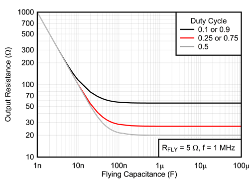
I described in my last post how RO reaches a minimum value when the flying capacitor is larger than some critical value, and here it is again in Figure 2. The main difference when using the switch node to drive a charge pump is that the duty cycle of the DC/DC converter has an effect on the value of RO(min), which increases whenever D moves away from 0.5 (see Figure 3). These parameters change too:

  • Peak current during the charge phase is   and during the discharge phase is  .
  • Output voltage ripple is  .

Figure 2: Output impedance vs. flying capacitance

Figure 3: The effect of duty cycle on RO(min)

For all practical purposes, the output impedance of the switch node is close to zero. Which is good, right? Actually, it’s not, because very low drive impedance can cause high peak currents to flow into the switch node, which can sometimes screw up boost converter operation. This is especially true during startup, when the flying capacitor must charge up over a number of cycles from 0V to almost 15V. To get around this, it is good practice to include a resistance of a few ohms (RFLY) in series with the flying capacitor, in which case the minimum output resistance is 

Of course, you can use the switch node equally well to generate negative output voltages (see Figure 4).

Figure 4: Boost converter driving an inverting charge pump

The math for this circuit is similar to the voltage doubler case:

 where once again 

There are various ways to regulate the output voltage of a discrete charge pump, but the easiest by far is to let the charge pump run open loop and simply post-regulate with a linear regulator. There’s no efficiency hit using this method – all but the most sophisticated charge pump regulation techniques burn off unused power – and it’s easier to stabilize. The alternative circuit shown in Figure 5 is attractive because you can use a positive regulation circuit to control a negative output voltage, but regulating the charge pump’s output voltage directly in this way often causes the charge pump’s control loop to “fight” with the boost converter’s control loop. One way to solve this problem is to make sure that the charge pump’s crossover frequency is much lower (at least five times lower, say) than the boost converter’s. Using a linear post-regulator avoids this problem altogether.

Figure 5 – Regulating an inverting charge pump

The examples in this post show charge pumps running from the switch node of a boost converter, but you could of course use other converter topologies. The main advantage of the switch node in a boost converter is that its amplitude is constant. This is not the case when using the switch node of a buck or buck-boost converter, in which the amplitude varies with the input voltage. Of course, if you’re running from a regulated input voltage you won’t have this problem, whichever topology you use.

Correct charge pump operation relies on the drive signal being permanently available. This is not guaranteed if the charge pump runs from a converter that uses a pulsed-frequency mode (PFM) at low output currents to improve efficiency. During PFM operation, a DC/DC converter switches in bursts; during the pauses between switching bursts, the charge pump’s output voltage will decay because its output capacitor has to supply all of the output current. It’s much better if the DC/DC converter driving the charge pumps continues to operate in pulse-width modulation (PWM) at all times.

Similarly, correct charge pump operation can be disturbed if the boost converter inductor current ever goes discontinuous, in which case the charge pump’s drive signal disappears. If the boost converter’s output current is high enough, inductor current may stay continuous. Alternatively, if the converter uses synchronous rectification, the inductor current may stay continuous, even at low output currents. (Take care, however: Some synchronous converters, particularly those aimed at low-power applications, turn off the synchronous rectifier when the inductor current is zero and enter discontinuous conduction mode (DCM)).

In the final installment of this series, I’ll take a look at multistage charge pumps.

Additional resources:

  • Read part 1 of the “Pump it up with charge pumps” series
  • Read part 2 of the “Pump it up with charge pumps” series


DC/DC converter datasheets - Quiescent current demystified: Part one

$
0
0

One of the most confusing specifications of a DC/DC converter is its quiescent current, or IQ. Part of the reason for this is that each manufacturer uses different terminology and definitions to specify the same thing – at least it seems that way to someone who may not be familiar with the detailed operation of a switching regulator.

 In part 1 of this two-part series, I’ll focus on the current required from the input supply that flows into the input voltage (VIN) pin of a buck (step-down) regulator. When reading through the data sheet (and you must always read your data sheet!), it is best to focus on the conditions under which the input current was taken rather than get caught up in the terminology. Let’s look at three of the most important supply currents in which a typical user would be interested.

 “Shutdown current” usually refers to the supply current measured when the regulator shuts off. Under these conditions, the output from the regulator is 0V with the nominal input voltage present, and whatever voltage the enable pin requires to shut down the converter. It may seem strange that any current is required when the regulator is off, and in fact many converters draw only small leakage currents when they are off.

 However, some regulators need to monitor the input voltage or a precision-enable input even when in shutdown mode. These functions require a finite amount of bias current to power the internal circuits – a parameter that’s important when a battery powers the regulator (such as in automotive or portable applications). This shutdown current will be the smallest current drawn from the input supply.

 A somewhat more confusing term is “non-switching” current. This refers to the input supply current when the regulator is enabled but not producing an output voltage. Non-switching current is usually measured open loop, with the voltage on the feedback pin high enough to stop the regulator from switching, producing no output voltage.

 You may ask, “Why would I care about the current drawn when the regulator is on but not producing a useful output?” The simple answer is that you shouldn’t care, since these are not conditions used in the application of the regulator. But there are at least two good reasons why this specification shows up in the data sheet. First, with the regulator in a known state, non-switching current is a good measure of the health of the internal circuits and easily measurable in a production environment during the manufacturing of the integrated circuit (IC). Secondly (and more important), this current is part of the total supply current that the regulator uses when operating at no load.

 A more useful supply-current specification is the operating current required at no load. In this condition, the converter is regulating the output voltage but the load current is zero. Many systems require the presence of a regulated voltage while in standby, and in this condition you need to know how much current will be required from the input supply. Most modern regulators specify this current in the data sheet. However, check the conditions carefully to be sure that the current listed is actually the no-load operating current.

 In the second part of this series, I’ll take a look at the no-load operating current in more detail, including what its definition includes.

 Additional resources:

Power Tips: Simplify creation of multiphase and multimodular board designs with Altium

$
0
0

As the demand for automotive and industrial power increases, so does the need for multiphase and modular-based designs. Designing a multiphase or multimodule board can be tedious and take a long time. In this Altium tips blog, I will show you how to easily copy and paste an existing schematic and layout to create a multiphase or multimodule designs.

Step No. 1: Build a simple buck-converter schematic in Altium (Figure 1).

 Figure 1: Altium schematic

Step No. 2: Update the printed circuit board (PCB) and layout the components. Pour the polygon pours as normal and connect all of the nets (Figure 2).

Figure 2: Layout in Altium

Step No. 3: Select the components you want to copy by clicking and dragging; then right-click and select Copy (Figure 3).

Figure 3: Screenshot of step No. 3

After copying, Altium will ask for a reference point; click a specific component.

Step No. 4: Paste the new components next to the existing components, as shown in Figure 4. Altium will add “_1” next to each reference designator to signify that it’s a copied component.

Figure 4: Layout in Altium showing copied components

Now that you’ve successfully copied the components into the layout, you’ll need to do the same in the schematic window and then link the components.

Step No. 5: In the Projects window, right-click the project name and click Add New to Project; then click Schematic (Figure 5). This will give you a new schematic sheet to copy components into.

Figure 5: Screenshot of step No. 5

Step No. 6: Copy and paste the schematic in Figure 1 to the new sheet. You will have to add “_1” to all of your new components before you can link the schematic with the current layout. To do that, you can use the Smart Edit option in Altium.

Step No. 7: Right-click U1 (new sheet) and select Find Similar Objects (Figure 6). Click OK in the pop-up menu.

Figure 6: Screenshot of step No. 7

Altium will highlight all of the components on the schematic and open the SCH Inspector window.

Step No. 8: Click the “…” button to the right of Component Designator (Figure 7).

Figure 7: Screenshot of step No. 8 

Step No. 9: In the Smart Edit window, click the Formula tab (Figure 8).

Figure 8: Screenshot of step No. 9

Step No. 10: In the Apply formula field, type “! + '_1'” (no quotation marks) and click OK (Figure 9).

Figure 9: Screenshot of step No. 10

Altium will add “_1” to the existing reference designators. This will now match your layout (Figure 10).

Figure 10: Revised schematic

Step No. 11: While in the schematic window, update your PCB (Design > Update) to see the net(s) appear, as in Figure 11.

Figure 11: Revised layout in Altium

You must also add “_1” to any nets where you don’t want the modules to share. Follow the same Smart Edit procedure.

Step No. 12: Right-click any net labels. Select Find Similar Objects and click OK (Figure 12). After Altium highlights all of the nets, click off of any nets you want the modules to share, like VIN, etc.

Figure 12: Screenshot of step No. 12

Step No. 13: In the SCH Inspector window, click “…” to the right of Text (Figure 13).

Figure 13: Screenshot of step No. 13

Step No. 14: In the Smart Edit window, click in the Apply formula field and type ! + ‘_1’. Click OK (Figure 14).

Figure 14: Screenshot of step No. 14

All of the nets will now have “_1” next to them, signifying that they are from your original module. Your new schematic sheet will look like Figure 15.

Figure 15: Revised Altium schematic

Step No. 15: Update the PCB; you’ll see new net names (Figure 16). The only net shared between the two modules/phases is now the GND net.

Figure 16: Revised layout in Altium

Polygon pours will copy over, but you will need to rename them to the new nets (Figure 17).

Figure 17: Revised layout in Altium

These steps should save you substantial time when making multiphase or multimodular PCBs in Altium and help designers get their products to market faster.

With current-sharing designs in particular, the smallest of differences in layout can lead to nonequal sharing. So another great reason to use this copy-and-paste trick is that it helps reduce the small differences that can come from individual component placement.

Additional resources

Differences between PSR and SSR in bias power-supply design

$
0
0

For a bias power supply with a power level less than 10W, the biggest consideration about the design is its efficiency and its cost. In this post, I’ll compare two control schemes – primary-side regulation (PSR) and secondary-side regulation (SSR) – and offer some suggestions for how to get a more efficient and cost-competitive design.

The classic flyback topology shown in Figure 1 is still the most popular for power levels less than 10W, not only because its few external components can help you get a very competitive bill-of-materials (BOM) cost, but also because a flyback topology can easily realize multiple outputs, which is the key specification for a bias power-supply design.

 Figure 1: Classic flyback topology

Secondary-side regulation

Figure 2 shows a typical SSR control block diagram. In order to stabilize the output voltage, the feedback from the output voltage is needed. For safety, isolated power supplies require non-galvanic feedback; the output must be electrically isolated from the AC input. Traditionally, an optocoupler transistor provides this isolation. Compared to the classic flyback topology, the key difference is adding an optocoupler such as the TI TL431, along with several resistors and capacitors, to constitute the feedback loop and error-amplifier-compensated circuit.

Figure 2: Typical SSR flyback block diagram with single output

With optocoupler feedback, it is possible to choose which output to regulate, or to weight the impact each output has on loop demand by connecting a sense chain from each output, as shown in Figure 3. So you can easily get load regulation within ±1% if you used the SSR control law.

 Figure 3: SSR block diagram with multiple outputs


Primary-side regulation

Compared to an SSR topology, the PSR control method eliminates the optocoupler and compensated components (as shown in Figure 4). The magnetic field in the transformer provides the feedback. Although resistors and capacitors are pretty cheap (but error amplifier and optocoupler cost are not insignificant), this method does save cost and printed circuit board (PCB) area. The optocoupler’s aging characteristics will reduce the reliability of the design, so fewer components can increase mean time between failures (MTBF).

In the other hand, PSR controllers are typically internally compensated, which can save time and effort for control-loop design. For applications with high surge or isolation voltage requirements, reducing the number of components crossing the isolation barrier reduces the number of areas that could potentially break down.

For a PSR controller’s crossing regulation, the most heavily loaded output sets the loop demand. The other outputs may be poorly regulated if lightly loaded. And because most PSR controllers use “knee point sampling” for feedback, the controller only operates in discontinuous conduction mode (DCM). The output voltage ripple will be higher than in continuous conduction mode (CCM).

Figure 4: PSR block diagram with single output

Table 1 compares some key features between PSR and SSR control law.

Table 1: Quick comparison of key features between PSR and SSR control

New reference design

The Universal Input, 10-W, High Efficiency, Low-Cost Power Supply with Isolated Multiple Inputs reference design is designed for bias power of appliances, operating in constant-voltage (CV) and constant-current (CC) flyback using TI’s UCC28911 controller. That high-voltage switcher integrates a high-voltage power FET plus a controller that uses PSR, supporting magnetically sensed output voltage regulation via the transformer bias winding. The sensing eliminates the need for a secondary-side reference, error amplifier and optical isolator for output-voltage regulation. The magnetic sampling scheme allows operation only in DCM, so the device is not allowed to turn on the power FET if it doesn’t sense a zero crossing detector (ZCD) event such as when the auxiliary winding voltage crosses zero from high to low after transformer demagnetization is complete. The modulator adjusts both frequency and peak current in different load regions to maximize efficiency throughout the operating range. Smart management of the control logic power consumption and the high-voltage current source, used for startup that is off during operation and has very low leakage current, allow you to design converters with very low standby input power.  

The key highlights of this reference design are:

  • More than 75% low load efficiency under 10% load
  • Less than 30-mW standby power under 90-V input
  • Valley Switching and Frequency Dithering to Ease EMI Compliance

 Figures 5 and 6 show a simple schematic and efficiency curves, respectively.

Figure 5: Multiple-output flyback converter based on the UCC28911

Figure 6: Efficiency curves at 230VAC and 115VAC inputs

Summary

The flyback converter is the most popular topology for low-power isolated power supplies. While easy to realize multiple outputs with low cost, this topology still has poor transformer utilization and high AC resistance losses.

If you want to achieve good transient response performance and need a high-accuracy output, the SSR control topology is more suitable. If the design is very sensitive to cost and standby power consumption, choose the PSR controller.

Additional resources

DC/DC converter datasheets - Quiescent current demystified: Part two

$
0
0

At the end of part 1, I started talking about the no-load input supply current. But there is one more “quiescent” current that you need to look at before I continue.

Many DC/DC converters have an internal low dropout regulator (LDO) that supplies power to the converter’s internal circuits. In modern regulators, the input of the LDO is often available as an external pin on the converter. It is usually called “bias,” but check the data sheet to be sure that you have the right pin. With this input connected to the output of the regulator, the bias current acts as an extra load on the output of the converter. The load is down-converted just like any other load by the ratio of input voltage to output voltage. This is the preferred connection, since it reduces the current at the input and therefore improves efficiency.

Now let’s get back to the no-load input current. Sometimes you may not find this input current in the data sheet, or it is not specified under the conditions you’re interested in. In that case, you can use Equation 1 to estimate the no-load input current for a buck regulator:

 This equation gives you a best-case estimate, since it does not take into account the losses in the converter. The first term, labeled IQ, is the non-switching quiescent current I talked about in the previous installment. The next term, IEN, is the current going into the regulator’s enable input. Many converters require a finite amount of bias current flowing into the enable input. If the enable pin is connected to the input supply to turn on the regulator, then you must account for that current; otherwise it is zero. The IDIV term is the current in the feedback divider and is easily calculated using Equation 2:

The term IB represents the current flowing in the bias input that I just talked about. Let’s use the SIMPLE SWITCHER® LM43603 3.5V to 36V, 3A synchronous step-down voltage converter as an example. The data sheet has these typical values (Table 1).


 Table 1: LM43603 Data Sheet

If you are converting a 12V input to a 3.3V output, with a total feedback divider resistance of 1MΩ, Equations 1 and 2 give you the following value for the no-load input current:

Notice that, for the LM43603, the data sheet presents the no-load input current at one typical condition, as shown in Table 1.

My calculated value of 30µA is somewhat different, but it is close enough for a rough estimate.

The equations here are meant to show you how the no-load input current depends on the input voltage, output voltage and other “quiescent” currents. You can see that the input current will increase for larger output voltages and smaller input voltages. So the best thing to do is to use the equations to estimate the no-load input current and then measure the actual value under the real application conditions.

You can also calculate the input current of a DC/DC converter by using the efficiency curves, but not at no load. By definition the efficiency is zero at no load, so you must use the method I’ve outlined in this post to estimate the no-load supply current. At any other load, you can use the efficiency curves in the data sheet, along with Equation 3:

where η is the efficiency under the conditions of interest.

Taking an example from the SIMPLE SWITCHER LM22670 3A step-down voltage regulator data sheet, the efficiency is about 91% for an input voltage of 5.5V and an output voltage of 3.3V at a load of 1.5A. That gives you an input current of about:

Using and estimating the input currents found in data sheets is not difficult, as long as you make sure that the values you are looking at are applicable to your specific application conditions.

Additional resources:

Power Tips: How to find switching loops in a power supply

$
0
0

Power-supply layout is one of the most important parts of being able to create a successful power design. Everyone has an opinion on how to do it and reasons why their way is the best way. The truth is that many different solutions will work; unless you really make a mess of the layout, the supply will probably function.

Of course, there are some universal rules, like:

  • Don’t run sensitive signals under fast-switching signals In other words, don’t run the feedback trace under the switch node.
  • Make sure that the power-carrying traces and planes are large enough to support the current.
  • Try to keep at least one continuous ground plane.
  • Use enough vias (typically 1A per via is a good place to start) to connect planes together.

Beyond these basic layout rules, I always start first by identifying the switching loops and then identifying which ones will have a high-frequency switching current. Figure 1 shows an example of a simplified power stage for a buck power supply (schematic and layout).

 Figure 1: Buck power-supply schematic and layout

In a buck power supply, there are two states (assuming continuous conduction mode): when the control switch (Q1) is on and when the control switch is off. When the control switch is on, current flows from the input to the inductor. When the control switch is off, current continues to flow in the inductor and through the diode (D1). The current is continuous to the output.

There is pulsing current on the input, however, and that’s the portion of the layout you need to pay attention to. In Figure 1, this loop is labeled “High Frequency Loop” and is shown in blue. Your primary objective of the layout should be to connect the Q1, D1 and input capacitors with the shortest, lowest inductance loop possible. Making this loop small will minimize noise generated by the switching. If you neglect to do this, the supply will not work very well.

The procedure for identifying the switching loops applies to all power-supply topologies. Step by step, the procedure is to:

  1. Identify the current paths during the on state.
  2. Identify the current paths during the off state.
  3. Find where the continuous current exists.
  4. Find where the discontinuous current exists.
  5. Minimize any loop that has discontinuous current.

This list shows the critical loops for a given power-stage configuration:

  • Buck – input capacitor loop.
  • Boost – output capacitor loop.
  • Inverting buck-boost – input and output capacitor loops.
  • Flyback – input and output capacitor loops.
  • Fly-Buck™ - input capacitor loop.
  • SEPIC – output capacitor loop.
  • Zeta – input capacitor loop.
  • Forward, half bridge, full bridge – input capacitor loop.

Power-supply layout is an art form. Everyone has their own way of doing it, and most of the time that is OK. Just make sure that when you are looking at placing the parts for a power stage, you identify the high-frequency switching loop; you will save yourself some time and headaches down the road.

Additional resources

DC/DC converter datasheets – System efficiency demystified

$
0
0

With the variety of regulators on the market, it can be difficult to choose a DC/DC regulator. Most automotive applications require high efficiency over the entire load range since they’re running from the battery. But then again, many industrial applications require good efficiency at high loads and efficiency at light loads is not very important. Understanding the losses in a DC/DC regulator is therefore important. Reading the efficiency curves in DC/DC converter data sheets also generates a few questions, such as “Why is the efficiency at light loads low?” and “Why does the efficiency dip at heavy loads?” In this blog series, I will attempt to deconstruct system efficiency into different component losses using the SIMPLE SWITCHER® LM2673 3A step-down voltage regulator as an example.

Figure 1 shows the evaluation module (EVM) schematic.

 Figure 1: Design schematic

Gate charge and IC losses

In a typical nonsynchronous buck regulator such as the LM2673, the power-dissipating components are the IC itself, the inductor and the catch diode. The root-mean-square (RMS) currents through the input and output capacitors and the parasitic equivalent series resistance (ESR) are very low; thus you can ignore the losses in those components.

Due to their construction, every MOSFET has some parasitic capacitance between its terminals. They are the gate-drain capacitance (CGD), gate-to-source capacitance (CGS) and drain capacitance (CDS), as shown in Figure 1. The capacitance values differ based on MOSFET size, fabrication and other process parameters. Unlike in an ideal MOSFET – where there are zero transition times – the presence of these parasitic capacitances introduces finite switching times, as shown in Figure 2.

Figure 2: MOSFET parasitic capacitances

The finite switching times, as shown in Figure 3, are a result of the charging and discharging of the input capacitance (CISS). The input capacitance is basically the addition of CGS and the Miller capacitance (CGD). The gate charge (QG) is the addition of the gate-to-source charge (QGS) and the gate-drain charge (QGD). The gate charge of the MOSFET is the charge needed to completely turn the MOSFET on. 

Figure 3: Gate charge and miller plateau

The MOSFET drivers provide the current (ICC) which you can estimate using Equation 1:

Where, FSW is the switching frequency of the DC/DC regulator.

For a converter like the LM2673, which has an integrated high-side MOSFET, the data sheet doesn’t list parameters like QG. Therefore, you’ll need to estimate the ICC in a different way: on the lab bench. With the device enabled and the load disconnected, measure the input current. Without a connected load, this input current measurement is essentially the ICC current measurement. The current ICC is also called the operating quiescent current. Please refer to the link in the ‘Additional Resources’ section to learn more.

For more accurate calculations, you can use TI’s WEBENCH® Power Designer software. WEBENCH Power Designer has information on all internal MOSFET parameters and therefore can take those into consideration while calculating losses.

As you can see from equation 1, the current is directly proportional to the switching frequency (FSW). Since the MOSFET driver is providing this current, there are losses in the driver. The driver voltage (VCC) is set by the internal low-dropout regulator (LDO). The losses in the driver are expressed as shown in Equation 2:

Since the LDO internal to the DC/DC regulator provides this current, there will be power dissipation in the LDO as well. This power dissipation is expressed as Equation 3:

If you add up Equations 2 and 3, you’ll get the total power dissipation of the LDO and the driver (Equation 4):

Therefore, with higher input voltages, the loss increases. Also, the gate charge directly affects the switching losses. If the internal MOSFET has larger parasitic capacitances, then the resulting gate charge will be larger; the time spent in the switch transition will also be a bit longer. This will consequently increase the switching losses.

In the next installment of this series, I’ll explain how the gate charge is related to the switching losses in the MOSFET, how the light load efficiency is dependent on these losses, and how the total losses affect the conduction losses and overall efficiency of a DC/DC regulator.

Additional resources

Have you been had? Check the stated vs. actual current limit

$
0
0

TI’s SIMPLE SWITCHER® LM257x and LM259x regulators have been a popular choice for direct current (DC)/DC buck regulation for over 20 years. Due to their popularity, a number of manufacturers have created similar products that seem to mirror SIMPLE SWITCHER products, yet they may not. Here’s what to look for when you are choosing between seemingly identical products.

Other manufacturers have created pin-to-pin (P2P) drop-in alternative devices for TI’s SIMPLE SWITCHER LM257x and LM259x families. These similar products – let’s call them “regulator X” – claim to have identical performance and specifications. But what you can’t see under the shell is that regulator X contains silicon designed for a completely different regulator, and the manufacturer has modified the pinout to match the SIMPLE SWITCHER configuration. The reality is that it is very difficult to match the exact parameters of a part with different silicon. This means that regulator X will have to de-rate its data-sheet specifications compared to the SIMPLE SWITCHER device, or else its performance will not match those specifications.

The data sheet for regulator X closely resembles the data sheet for TI’s SIMPLE SWITCHER regulator; in fact, it may look identical. But how well does the performance of regulator X match the critical parameters stated in its data sheet, like switching frequency and current limit? Good question. As a test, the applications engineering team at TI created a custom evaluation board to take performance and reliability bench data on TI’s SIMPLE SWITCHER 40V, 3A LM2596 buck converter, as well as three other regulator X devices – which I’ll call Xa, Xb and Xc – from various manufacturers.

We evaluated all four devices for efficiency across input voltage and load current for a common 5VOUT application. We conducted tests at temperatures of -40°C, 25°C and 85°C. We also tested output current all the way to 7A on the nominal 3A devices in an effort to reveal performance limits, safety risks and reliability risks. We took oscilloscope screen captures at each operating point and recorded thermal-camera images during short-circuit conditions.

The most common performance inaccuracy we found was in the stated vs. actual current limit. High current limits cause excessive inductor, diode and integrated circuit (IC) heating during short-circuit conditions, which can damage the IC and prevent it from functioning correctly. This in turn can prevent the end product from functioning. On the datasheets for regulators Xa, Xb and Xc, the stated current limit is 4.5A (typical). However during evaluation, we found that regulators Xa, Xb and Xc’s current limits actually ranged from 5A to 10A; see Table 1.

Table 1: Current-limit comparison between TI’s SIMPLE SWITCHER LM2596 and alternative devices

All three of the P2P-alternative ICs we evaluated had very high current limits that were well above their data sheet’s stated parameter. Two devices did not limit current until it was between 5.5A to 6A, while  another device reached currents all the way up to 10A during a short-circuit condition. As shown in Figure 1, this particular IC heated all the way up to 110°C and the diode (not pictured) heated up to 133°C. At those temperatures, the potential for IC damage is high.

Figure 1: Thermal-camera image of regulator Xc during a short-circuit condition

An accurate and safe current limit is essential for the long-term reliability of the end equipment in which these devices are used. A short-circuit condition can cause the system to become inoperable.

So the next time you are shopping for LM257x and LM259x regulators, remember that it takes more than copying a data sheet to create a quality IC. Select TI’s SIMPLE SWITCHER regulators and rest easy knowing they will perform to spec: We guarantee it.

Additional resources:

  • Thermal management is a major concern for any power designer. Select a SIMPLE SWITCHER DC/DC switching regulator with thermal resistance as low as 10°C/W.  


DC/DC converter datasheets – System losses demystified

$
0
0

Welcome back to the DC/DC converter datasheets series. Whereas in the last installment I covered system efficiency, in this installment I will discuss DC/DC regulator component switching losses, starting with what was Figure 3 in part 1 (Figure 1 here): the image of the VDS and ID curve against time.

Figure 1: Switching losses

Let’s first look at the switching losses in the integrated high-side MOSFET. At the beginning of every switching cycle, the driver starts supplying current to the gate of the integrated MOSFET. From part 1, you know that the MOSFET has parasitic capacitances across its terminals. During the first time period (t1 in Figure 1), the gate-source voltage (VGS) is approaching the MOSFET’s threshold voltage, VTH and the drain current is zero. The power loss during this period is therefore zero. In time period t2, the parasitic input capacitance (CISS) of the MOSFET begins to charge and the drain current starts flowing through the MOSFET, increasing linearly. For a buck topology, this current is the load current and the drain-source voltage (VDS) is the input voltage (VIN). Therefore, during the second time period (t2), there is a power loss that can be expressed as Equation 1:

Once the input parasitic capacitor of the MOSFET is charged, the load current flows through the MOSFET and VDS starts to fall. This time is also called “Miller time” because this time is spent just charging the Miller capacitance (CGD). During Miller time the drain current is constant at IOUT and VDS is falling from VIN. The power loss during this time is expressed as Equation 2:

Adding the total switching loss results in Equation 3:

Notice that in Figure 1, t2 is considerably shorter than the third time period (t3). Therefore in the equations, you could estimate the loss as just those in the time period t3. These finite transition times occur twice in a period: once when the MOSFET turns on (charging the parasitic capacitance) and once when it turns off (discharging the parasitic capacitance). Therefore, estimating the time t3 in both cases as the rise and fall times of the MOSFET, you can estimate the switching loss using Equation 4:

The switching loss is frequency- and input voltage-dependent. Therefore, at higher input voltages and switching frequencies, the overall efficiency is comparatively reduced. At light loads, the LM2673 nonsynchronous buck regulator enters discontinuous conduction mode. In this mode, the device still maintains the switching frequency. With every cycle, power is still dissipating inside the integrated circuit (IC). Therefore, even though conduction loss is not a factor at light loads, due to the always-present switching loss, device efficiency is affected. And since the average power delivered to the output is very low, the overall efficiency of the device is also low.

Newer regulators from the SIMPLE SWITCHER® family now come equipped with pulsed frequency modulation (PFM) that lowers the switching frequency when the load is reduced. This enables the regulator to maintain high efficiency all the way down to very light or no loads.

Because the LM2673 is a nonsynchronous device, it has a catch diode that gets forward-biased when the MOSFET turns off. The same principle of a non-zero transition time applies to the catch diode as well. But the voltage swing of the diode is just from ground to the forward voltage drop (VF) of the diode, making the switching losses in the diode negligible. You can also ignore switching losses occurring in the inductor’s core because SIMPLE SWITCHER regulators like the LM2673 have a comparatively lower switching frequency of 250 kHz.

In the next (and final) installment in this series, I will discuss the conduction losses in the MOSFET and passive components of the DC/DC regulator circuit, and present an expression for total losses and resulting efficiency.

Additional resources

From blue light to green power

$
0
0

Whizzing across the Japanese countryside at 300kph, my colleague Tomomasa Emoto and I arrived at Nagoya station by Shinkansen. Nagoya is home to famous Shintō shrines and castles, but that is not why we were there. We had the pleasure of visiting Professor Hiroshi Amano at Nagoya University. Amano-sensei  won the 2014 Nobel Prize in physics, along with Isamu Akasaki and Shuji Nakamura, for the invention of efficient blue light-emitting diodes (LEDs). Their invention has enabled bright and energy-saving white-light sources.

Once at Nagoya University, we made our way to Amano-sensei’s office. At the entrance to the wing, we exchanged our shoes for clean slippers; I’m told this is quite typical in Japan. Amano-sensei warmly greeted us and welcomed us into his office, and we had the pleasure of hearing the perspectives of a Nobel Prize winner on gallium nitride (GaN).

Figure 1: Texas Instruments’ Tomomasa Emoto, left, and Sandeep Bahl, center, pose with Professor Hiroshi Amano while visiting Nagoya University

While many of us are working to establish the “present” of GaN, Amano-sensei is working to define the future. Now with GaN LED work in good industrial hands, he has taken on a new challenge: how to unlock the full potential of the material. Today’s commercial GaN, he explained, is not perfect, and it is difficult to grow thick material. As a result, devices can only harness about a third of their high-field capability. By focusing on inexpensive ways to grow high-quality bulk material and by looking at different structures, it  is possible to make devices that operate closer to the material limit. These devices will not only be smaller but also higher voltage. Silicon carbide will have a hard time competing against GaN,  he explained, when low-cost high-quality bulk GaN growth becomes available.

GaN wasn’t always this popular. I was interested to know how Amano-sensei had the insight to work on GaN at a time when the world had given up on it, so I asked. “The world needed a blue LED,” he explained, “and most people were working on zinc selenide. I did not like it, because it was very brittle. I could drop GaN and nothing would happen, so I knew it would be more stable.”

As we left, slipping our shoes back on, I was glad to know that a Nobel Prize winner is thinking about the future of GaN devices. I can now go back to my world of working towards a more energy-efficient future, where I make sure that TI GaN devices, such as the LMG3410, operate reliably under actual-use conditions.

Additional resources:

Digitally select your reference voltage

$
0
0

Adjustable voltage references offer great flexibility to circuit designers because the reference is not limited to the manufacturer’s pre-set values. The adjustable output is typically configured with a voltage divider from the output to the feedback pin, as shown in Figure 1. To regulate the output, compare the voltage at the feedback pin to an internal reference (shown in this post as VREF_INT), typically 1.2V. The device adjusts the output until VFB and VREF_INT match.

Some adjustable shunt references such as the LM4041 maintain VFB across R1; some maintain VFB across R2, such as the TLV431. I’ll concentrate on the LM4041, but the concepts apply equally to other adjustable shunt references by switching R1 and R2 in the equations. In this blog post, I’ll describe one possible method of changing the resistor divider and in turn changing the reference voltage with digital signals.

Figure 1: Typical VREF feedback divider

The method involves replacing the two fixed resistors with a single digital potentiometer. Figure 2 demonstrates this conceptually, where the feedback pin is connected to the wiper of the potentiometer and the high and low side are connected to VREF and GND, respectively.

 Figure 2: Potentiometer center tap (wiper) connected to feedback

Figure 3 shows the circuit redrawn, with the TPL0102 digital potentiometer acting as the voltage divider. You can configure a digital potentiometer to act as a voltage divider by connecting a voltage across the high and low pins of the internal resistor and connecting the output to the wiper pin. The wiper position affects the ratio of the resistance between the wiper and the high and low pins, and its position is controlled digitally by sending a code word to the device. The TPL0102 uses an I2C interface, while other potentiometers are available with serial peripheral interface (SPI) or parallel interfaces.

 Figure 3: VREF with the TPL0102 digital potentiometer as the feedback divider

Because the ratio of the resistances sets the output voltage, the absolute values of the divider resistors are not critical. This allows you to easily replace the resistor divider with a digital potentiometer. Equation 1 illustrates the relationship between the adjusted output, VREF_OUT and the resistance ratio:

That is an important point in this application, as the absolute resistance value of digital potentiometers can vary quite a bit, while the ratio of the resistances is very accurate. For example, to generate a 3.3V reference voltage, the required resistance ratio of R2-to-R1 is 1.66.

The potentiometer data sheet provides the formulas to calculate the output of the voltage divider for a given code, shown in Equations 2 and 3. VHW is the voltage from the high pin (H) to the wiper (W), while VWL is the voltage from the wiper (W) to the low pin (L):

VFB is across R1, as I mentioned in the introduction, so let’s continue with Equation 2, which calculates the voltage between the high pin and the wiper pin. The wiper is connected to the feedback pin of the device, and VFB is forced to VREF_INT. Equation 4 shows the formula solved for the digital code required for VREF_OUT:

Continuing the example in Equation 5 where NTAPS is 256, VREF_INT is 1.24V and V­REF_OUT is 3.3V, you’ll need to write decimal code 160, which yields resistance values for R1 and R­2 of 37.50kW and 62.50kW, respectively. More importantly, the ratio of these two resistances is 1.66, also calculated using Equation 1:

If you need to change the reference voltage, you simply need to write an I2C transaction to move the wiper position accordingly. As a result, the voltage at the feedback pin changes and adjusts VREF_OUT. You can also use the potentiometer to digitally tune the reference voltage, where the greater the number of taps in the potentiometer, the finer the resolution in the resistance ratio and therefore the finer the resolution in the output reference voltage.

A limitation of using a digital potentiometer in this application is the voltage limit of the digital potentiometer integrated circuit (IC), which typically cannot exceed 5.5V. Confirm that the resistance ratio does not get set to a condition that would present a VREF_OUT greater than 5.5V. For a 256-tap digital potentiometer and a shunt reference with an internal reference of 1.24V, the decimal code should not exceed 200. Figure 4 demonstrates the effect of the input code on the reference voltage for a 256-tap potentiometer and a 1.24V-referenced device.

 Figure 4: Reference voltage vs. digital potentiometer code

Enable and configure the potentiometer before powering the shunt reference to ensure that the resistor divider is correctly in place. If that is not possible, you can add a large resistance in parallel with the resistor that is not acting as the drop for VFB. That would be 1MW from the feedback pin to ground (across R2) for the LM4041, or 1MW from the feedback pin to the output (across R­1) for the TLV431.

To avoid an extra parallel resistance, you can configure the device with fixed R1 and R2 resistors and a digital potentiometer in series with one of them. You would then have to configure the potentiometer as a rheostat, shown in Figure 5. This configuration depends on the absolute resistance of the digital potentiometer, which is not as accurate as when using it as a ratiometric voltage divider, and requires feedback to the microcontroller for final digital-code selection.

 Figure 5: Fixed resistors with digital potentiometer as a rheostat

Now that you understand how an adjustable voltage reference sets it output voltage, you know how to use this to your advantage to change the output voltage dynamically.  If the application already uses a microcontroller, including a digital potentiometer can add some versatility to a seemingly simple part.

Additional resources

Charge it up with charge pumps – Part 4

$
0
0

To conclude this short series on charge pumps, I’d like to give you a few circuit ideas, to get you thinking about a basic charge-pump circuit as a building block adaptable to a wide range of applications. If your application needs a nonstandard solution, there’s a good chance you can cobble it together from a few simple components. 

Each stage of a charge pump increases the output voltage by approximately the amplitude of the switching waveform. If you want higher (or, in the case of an inverting charge pump, more negative) output voltages, you can cascade more than one charge-pump stage (see Figure 1).

Figure 1: Cascading multiple charge-pump stages

You can also combine regulated and unregulated charge-pump stages. Figure 2 shows such a circuit, in which can regulate the output voltage between approximately 15V and 30V.

Figure 2: Regulated charge pump with additional unregulated stage

Charge-pump circuits use DC voltages to set the voltage across the flying capacitor during the charge phase. If you have them available, you can use different voltages as the supply during the charge phase to improve conversion efficiency or extend the output voltage range.

Figure 3 shows a circuit that uses a 5V input voltage to generate an output voltage of approximately 19.3V from a 15V boost converter.

Figure 3: High-efficiency charge pump

Figure 4 shows a circuit that uses a –5V supply to generate –9.3V from a 5V boost converter.

Figure 4: High-efficiency inverting charge pump

Figure 5 shows a nifty little charge-pump circuit that employs a Dickson multiplier. This uses anti-phase switching waveforms to reduce the number of switching stages needed. In this application, standard logic gates generate a 5V rectangular waveform, which is used to drive the charge-pump circuit to generate an output voltage of approximately 18V (albeit with low current capability).

Figure 5: Using logic gates in a Dickson multiplier circuit

Charge-pump circuits are sometimes used to generate a bootstrap supply in DC/DC converter circuits, as shown in Figure 6. In this circuit, a capacitor connected to the switch node generates a voltage higher than the supply voltage, which enables the use of an N-channel FET for the high-side switch. N-channel FETs are smaller than the equivalent P-channel device, which results in improved performance or lower cost (or some combination of the two). Note that the arrangement shown in Figure 6 only works when the switch node is switching, so it tends only to be used in converters that operate in forced PWM.

Figure 6: DC/DC converter bootstrap capacitor

Charge pumps are useful circuits to have in in your armory. They're low-cost, simple and flexible. Many circuits already have a suitable clock signal available to drive the charge pump, and all you need is a suitable driver stage. For more demanding applications, TI offers a range of dedicated charge-pump devices that offer even better performance than a do-it-yourself charge pump can achieve.

Additional resources:

  • Read part 1 of the “Pump it up with charge pumps” series
  • Read part 2 of the “Pump it up with charge pumps” series
  • Read part 3 of the “Pump it up with charge pumps” series
  • Browse the charge pump portfolio

Keep it simple with an LDO regulator

$
0
0

Living and working in Asia exposes me to a wide variety of interesting support questions. For example, I was recently asked if TI had a cross-device to an LDO controller. This controller is in a small-outline transistor (SOT)-236 package that takes up a 3mm-by-3mm area on the printed circuit board (PCB). Figure 1 shows the recommended schematic for the controller. 

 Figure 1: Simple LDO controller

On the surface, the approach of  using a high-current regulator looks good. After learning the design engineer wanted to support a maximum 4A of current from 1.35VIN to 1.0VOUT, I recommended  the TPS7A85. The TPS7A85 is not a controller, but it is a fully integrated 4A LDO voltage regulator that comes in a 3.5mm-by-3.5mm 20-pin quad flat no-leads (QFN) package. Obviously, that package is a little larger than the SOT-236.

The immediate response was, “The TPS7A85 is too complicated.” There are cases where more pins equals more complexity; however, in the case of the TPS7A85, more pins actually translates into fewer components. See the equivalent TPS7A85 schematic in Figure 2, where the external component count decreases from nine to five.

Figure 2: The TPS7A85 as a 4A LDO

Why are there four fewer components? The TPS7A85 incorporates TI’s ANY-OUT feature, which allows users to dynamically set VOUT with voltage-setting pins. Whenever one of these pins is grounded, the voltage adds to the internal 800mV reference. So by grounding the 200mV pin, VOUT instantly becomes 1.0V.

With this feature, you can change the voltage from 800mV to 3.95V simply by grounding the appropriate voltage-setting pins to create the desired output voltage. The quantifiable benefits of this approach are:

  • 1% guaranteed output regulation.
  • No need to buy precision-feedback resistors to set VOUT (you can still use the FB pin with external resistors if you wish, of course).
  • The ability to dynamically set VOUT in the application.

With an LDO controller, the overall efficiency is only 1/1.35V, or 74%. The total power dissipation in the power FET is worst-case 4A ×4350mV, or 1.4W. Turns out, that is the same efficiency you get with an LDO regulator.

To manage the thermals, the controller uses two external FETs to help spread the heat, as shown in Figure 3.

Figure 3: An LDO controller driving two pass FETs

If you wish to do use a controller, I recommend adding another RGATE to help make sure the gate-drive layout is as symmetrical as possible so that Q1 and Q2 share the current properly. In this application, the FETs are in a 5mm-by-6mm package, which takes up more than six times the area of the controller itself.

The TPS7A85 package is only 3.5mm by 3.5mm, so its thermal performance may not be as good as the LDO controller. But let’s compare the difference. With the controller, the FETs have a temperature from junction to ambient thermal resistance (TJA) of 25°C/W. Thus, at peak current with the power dissipation at 1.4W, the temperature rise should be around 1.4W × 25°C/W, or 35°C. The temperature rise would be 17.5°C per FET – assuming that the FETs share the temperature rise evenly. That seems pretty robust. How does it compare to the TPS7A85?

The TPS7A85 has a TJA of 35.4°C/W, so at peak power the temperature rise is 1.4W × 35.4°C/W, or 49.6°C. On the surface this looks worse, but is it? Consider some of the real advantages that an integrated LDO regulator has over an LDO controller:

  • Thermal shutdown – The LDO controller does not have the ability to monitor the FET temperature. The TPS7A85 does.
  • Current limit – The LDO controller’s only job is to regulate VOUT. It has no ability to limit current or shut down when the load current is too high. The TPS7A85 does.
  • Stability – If you want to ensure that the LDO controller is stable with the FET(s) and parasitic capacitances and inductances in the application, you would have to add additional components to measure loop stability. With the TPS7A85, you would not.
  • Size – The LDO controller takes up a lot more area because of the external FET. The TPS7A85 does not.
  • Accuracy – The LDO controller in this application has an overall accuracy of 2.5%. When considering the external resistor’s worst case, this is 4.5%. The TPS7A85 overall accuracy is better than 1%.
  • Noise – The LDO controller does not even mention this on the data sheet.  The TPS7A85’s noise is ~5μVRMS 10-100KHz at 1VOUT.

The last two advantages in this list are worth highlighting, as most applications choosing an LDO controller or LDO regulator over a DC/DC converter are doing so to power precision VCORE rails for FPGAs or DSPs, or precision ADCs/DACs.

To sum it all up, the LDO regulator approach seems to be the simplest way to get the job done.  Consider TI’s TPS7A85 high-current, high-accuracy, low-noise LDO voltage regulator for your next design.  Order the TPS7A85evaluation module now.

Additional resources

Viewing all 437 articles
Browse latest View live


<script src="https://jsc.adskeeper.com/r/s/rssing.com.1596347.js" async> </script>