Quantcast
Channel: Power management
Viewing all 437 articles
Browse latest View live

How GaN enables high efficiency in totem-pole PFC-based power designs

$
0
0

Almost all modern-day industrial systems involve an AC/DC power supply, which takes energy from the AC grid and delivers it to electrical equipment as a well-regulated DC voltage. With power consumption increasing around the globe, the associated energy loss in the AC/DC power-conversion process becomes a significant component of the overall energy cost equation for power-supply designers, especially those working on power-hungry telecom and server applications.

Gallium nitride (GaN) can help increase energy efficiency and reduce losses in an AC/DC power supply, which in turn helps lower the cost of ownership of the end application. For example, by enabling an efficiency gain as little as 0.8%, GaN-based totem-pole power factor correction (PFC) can help a 100-MW data center save as much as $7 million in energy costs over 10 years.

Choosing the right PFC stage topology

Government regulations worldwide mandate the use of a PFC stage in the AC/DC supply in order to facilitate a clean power draw from the grid. A PFC shapes the AC input current to follow the same shape as the AC input voltage, which maximizes the real power drawn from the grid, making the electrical equipment act like a pure resistor with zero reactive power.

As shown in Figure 1, traditional PFC topologies include the boost PFC (with a full-bridge rectifier after the AC line) and dual-boost PFC. The classical boost PFC is a common topology that contains a front-end bridge rectifier that has very high conduction losses. The dual-boost PFC reduces conduction losses since it does not have a front-end bridge rectifier, but it does need an additional inductor, and thus suffers in terms of cost and power density.

Figure 1: PFC topologies: dual-boost PFC (b); boost PFC

Other topologies that may increase efficiency include AC-switch bridgeless PFC, active-bridge PFC and bridgeless totem-pole PFC, shown in Figure 2. The AC switch topology uses two high-frequency field-effect transistors (FETs) conducting during the on-state and one silicon carbide (SiC) diode, plus a silicon diode, conducting during the off-state. Active-bridge PFC simply replaces the diode bridge rectifier connected to the AC line with four low-frequency FETs, which require additional control and driver circuitry. Active-bridge PFC uses three FETs conducting during the on-state and two low-frequency FETs, plus one SiC diode conducting during the off-state.

In comparison, totem-pole PFC has just one high-frequency FET plus one low-frequency silicon FET conducting during both the on-state and off-state, offering the lowest power losses among the three topologies. In addition, totem-pole PFC requires the fewest number of power semiconductor components to implement, which makes it an attractive topology when considering overall component count, efficiency and system cost.


Figure 2: Various PFC switch topologies that increase efficiency


Benefits of GaN in a totem-pole PFC

Traditional silicon metal-oxide semiconductor FETs (MOSFETs) are not a good fit for totem-pole PFC, as MOSFETs have a body diode with a very high reverse-recovery charge, causing high power losses and the risk of shoot-through damage. SiC power MOSFETs represent a marginal improvement over silicon, with lower reverse recovery from the inherent body diode.

Alternately, GaN offers zero reverse-recovery losses, with the lowest overall switching energy loss among the three technologies – over 50% lower versus comparable SiC MOSFETs. This is primarily because of the higher switching-speed capability of GaN (100 V/ns or higher), lower parasitic output capacitance and zero reverse recovery. The lack of a body diode in GaN FETs eliminates the risk of shoot-through entirely.

TI recently worked with Vertiv on a design that helped achieve a 98% peak efficiency in their 3.5-kW rectifier, achieving a 1.7% efficiency gain compared to the 96.3% peak efficiency of their previous-generation silicon 3.5-kW rectifier. To extrapolate this efficiency benefit to a real example, the use of GaN-based totem-pole PFC enables a 100-MW data center to save as much as $14.9 million in energy costs over 10 years, along with the added benefit of reduced carbon dioxide emissions.

The lack of reverse-recovery losses and reduced output capacitance and overlap losses in TI GaN enabled Delta Electronics to reach up to 99.2% peak efficiency in energy-efficient server power supplies for data centers. The integrated gate driver inside the TI GaN FET allows the FET to reach switching speeds up to 150 V/ns, lowering overall losses at high switching frequencies and enabling Delta to achieve an 80% improvement in power density, while increasing efficiency by 1%.

The benefits offered by GaN technology in totem-pole PFC designs are undisputable. As more power-supply unit designers switch to GaN, and as GaN manufacturers release innovative products, telecom and server power designers can expect continuous improvements in power density and energy efficiency.

Additional resources


Key considerations for advancing satellite electrical power systems

$
0
0

Satellite power design has a complex set of trade-offs given that the design has more variables, and the number of semiconductor options are significantly smaller than those in commercial applications. A satellite’s primary power supply is especially important, since if it fails, there’s little to no opportunity for repair. And with the advancement of space-grade high-performance field-programmable gate arrays, satellites now have significantly higher local computing power, increasing overall power demands.

When developing any satellite electrical power system (EPS), two of the most important trade-offs are the overall thermal design and the mission profile radiation requirements.

Thermal management for system efficiency

Component selection, topology selection and switching frequency are all vital when determining the efficiency of a switched-mode power supply (SMPS). The thermal load of the system directly correlates to the efficiency of the power supplies and the dissipation of power losses throughout the satellite.

A satellite’s EPS must step down the voltages from the energy generation solar array portion of the system (typically 100 V ±50%) to the battery storage portion (typically 28 V ±20%), and then again to the clean point-of-load power supply (<5 V) for satellite payload cards such as single board computers, instrumentation or communication cards, or radar or communication cards. At each of these conversion stages, achieving the highest possible efficiency will help reduce power losses, as space power losses have far wider overall system and weight implications.

One technique to improve efficiency is synchronous rectification, where replacing a conventional power diode with a gate-controlled transistor significantly reduces the conduction loss of the power path. The forward characteristic of diodes, particularly those suitable for handling the current targeted by newer SMPS designs, often results in a larger voltage drop during the on-state. On the other hand, the synchronous rectification transistor is typically a field-effect transistor with a low on-state resistance, leading to much lower conduction losses at the same current level.

In a satellite’s EPS design, pulse-width modulation (PWM) controller-based architectures provide the greatest flexibility to support a range of power-supply topologies at the highest efficiency levels. The radiation-hardened TPS7H5001-SP PWM controller family and radiation-tolerant TPS7H5005-SEP PWM controller family both support synchronous rectification, configurable dead time and other integrated features that enable designers to create smaller and more efficient isolated or non-isolated power supplies. An adjustable duty-cycle limit of 50%, 75% or 100% allows designers to use a single controller in the implementation of DC/DC converter topologies and integrated synchronous rectification outputs enable fully synchronous versions of each topology without additional external circuitry, offering overall system size benefits. Configurable dead time helps optimize power converter efficiency, particularly for gallium nitride (GaN) power semiconductor-based designs. An adjustable leading-edge blank time enables configuration of the controller’s internal current sense based on the specific converter parasitic inductances and capacitances, as well as those for the printed circuit board or power module substrates.

Table 1 compares the different devices.

Feature

TPS7H5001-SP

TPS7H5005-SEP

TPS7H5002-SP

TPS7H5006-SEP

TPS7H5003-SP

TPS7H5007-SEP

TPS7H5004-SP

TPS7H5008-SEP

Primary output configuration

Dual

Single

Single

Dual

Synchronous rectification output configuration

Dual

Single

Single

N/A

Duty cycle limit supported

100%, 75%, 50%

100%, 75%

100%, 75%

50%

Programmability of output dead-time

Yes

Yes

No, fixed at 50 ns

No

Leading edge blank time support

Yes

Yes

No, fixed at 50 ns

Yes

Target GaN FET / Si MOSFET

GaN FET or Si MOSFET

GaN FET

Si MOSFET

GaN FET or Si MOSFET

Topology

Buck, boost

Yes

Yes

Yes

No

Flyback

Yes

Yes

Yes

No

Forward and active clamp

Yes

Yes

Yes

No

Push-pull

Yes

No

No

Yes

Half-bridge and full-bridge

Yes

No

No

Yes

Table 1: Comparing the TPS7H5001-SP and TPS7H5005-SEP PWM controller families

Mission profile radiation requirements

Because all flight hardware needs to understand the orbit of the satellite and its expected radiation exposure, it is not possible to select satellite devices without reviewing the mission radiation requirements.

Satellite electronics will experience three types of radiation effects while in orbit:

  • Total ionizing dose (TID) is an accumulated dose of radiation exposure over time. Prolonged radiation exposure can create trapped charges in the oxides of the semiconductor device, which in turn leads to parametric shifts within the device and eventually functional failure.
  • Single-event effects (SEEs) measure the effects of heavy ions of the device under test. High-energy ion strikes can generate electron-hole pairs that lead to nondestructive events such as single-event transients (SETs) or single-event functional interrupts (SEFIs). These ion strikes can also cause destructive effects such as single-event latch-up (SEL), single-event burnout (SEB) or single-event gate rupture (SEGR).
  • Displacement damage dose is another type of accumulating dose exposure that assesses damage to the crystal structure of the device from multiple ion strikes. While protons are typically the main cause of displacement damage in space, the neutron displacement damage (NDD) test uses neutrons because protons have TID effects; using neutrons makes it possible to separate displacement damage from TID effects.

It’s important to validate how a component will perform when exposed to these types of radiation, especially components in the power supply. The TPS7H5001-SP device family includes TID radiation reports up to 100 krad(Si) and NDD up to 1 × 10¹³ neutrons/cm2, ensuring that the device passes each of the automatic test equipment test vectors post-radiation exposure that device manufacturers use to guarantee underlying data-sheet limits. For the TPS7H5001-SP SEE testing, destructive SEE testing for SEL, SEB and SEGR immunity is confirmed to a linear energy transfer (LET) equal to 75 MeV-cm2/mg, with SET and SEFI characterized to a LET equal to 75 MeV-cm2/mg.

The TPS7H5005-SEP device family includes TID radiation reports up to 50 krad(Si) and NDD up to 1 × 10¹³ neutrons/cm2 with destructive SEE testing for SEL, SEB and SEGR immunity is confirmed to a linear energy transfer (LET) equal to 43 MeV-cm2/mg, with SET and SEFI characterized to a LET equal to 43 MeV-cm2/mg.

Conclusion

Supporting the latest high-performance computing solutions in today’s smaller satellites focuses a lot of attention on the thermal design challenges of the system. The new TPS7H5001-SP and TPS7H5005-SEP PWM controller families allow designers to achieve maximum power efficiency and design flexibility. To address the ever-present radiation requirements these two families of devices also have detailed radiation reports for TID, SEE and NDD that highlight how they can support any type of orbit or mission, be it low earth orbit, medium earth orbit or a geostationary orbit.

Additional resources

Download the TPS7H5005-SEP flyback converter calculator.

5 converter topologies for integrating solar energy and energy storage systems

$
0
0
Other Parts Discussed in Post: TIDA-01606, TIDA-010210

With energy storage systems prices becoming more affordable and electricity prices going up, the demand for renewable energy sources is increasing. Many residences now use a combined solar energy generation and battery energy storage system to make energy available when solar power is not sufficient to support demand. Figure 1 illustrates a residential use case and Figure 2 shows how a typical solar inverter system can be integrated with an energy storage system.

Figure 1: A residential solar energy generation and energy storage system installation

Figure 2: A typical solar inverter system with an energy storage system

In the best-case scenario, this type of system has highly efficient power management components for AC/DC and DC/DC conversion and high power density (with the smallest possible solution size) that are highly reliable (with the lowest losses) and enable fast time to market. Those requirements are not always achievable at the same time, however, and you will need to make trade-offs on the best power-conversion topologies for these subblocks.

What existing power topologies for AC/DC and DC/DC buck and boost power converters have in common are half bridges or converter branches that run interleaved, either to increase power levels in a DC/DC converter or to achieve three-phase operation in an AC/DC inverter or power factor correction stage by placing three branches running in 120-degree phase shifts. Figure 3 shows simplified schematics of five power topologies.

Figure 3: Power topologies for half-bridge and branch equivalent

  • Topology No. 1: In the two-level converter topology, pulse-width modulation (PWM) signals are applied complementary (with a dead-time delay to avoid shoot-through because of overlapping switching signals) to power devices Q1 and Q2. For the positive sine wave at the output, the duty cycle applied is >50% at Q1. For the negative sine wave at the output, Q2 has a >50% duty cycle. It is a simple concept to control the output power, but output signals before the line filter have a full bus voltage swing, which requires a larger filter to reduce electromagnetic interference. The ripple frequency into the filter is the PWM frequency, which affects the size of the filter.

Three-level topologies allow the use of smaller passive components and have lower EMI compared to two-level converters. There are four three-level topologies:

  • Topology No. 2: The T-type topology is named for the way that the transistors are arranged around the neutral point (VN). Q1 and Q2 connect between the DC link, and Q3 and Q4 are in series with VN. The ripple frequency seen by the filter is equal to the PWM frequency applied to switches Q1 through Q4. This defines the size of the filter components to achieve the required low total harmonic distortion at the AC line frequency. Q1 and Q2 see the full bus voltage and need to be rated at 1,200 V for an 800-V DC-link voltage in the system. Since Q3 and Q4 connect to VN, they see only half the bus voltage and can be rated at 600 V in an 800-V DC-link voltage system, which saves costs on this converter type. See the 10-kW, Bidirectional Three-Phase Three-Level (T-Type) Inverter and PFC Reference Design.
  • Topology No. 3: In the active neutral point clamped (ANPC) converter topology, VN connects with active switches Q5 and Q6 and sets VN in the middle between the DC-link voltage. Like the T-type converter, the ripple frequency seen by the filter is equal to the PWM frequency defining the size of the AC line filter. What’s nice about this architecture is that all switches can be rated at half the maximum DC-link voltage; in an 800-V system, you can use 600-V rated switches, which positively impacts cost. When turning off this converter, it’s important to limit all voltages across each switch to half the DC-link voltage. In other words, the control microcontroller (MCU) needs to handle the shutdown sequencing. TI’s TMS320F280049C and other devices in the C2000  product family have configurable logic that allows the realization of shutdown logic in hardware to offload software tasks for the MCU. See the 11-kW, Bidirectional, Three-Phase ANPC Based on GaN Reference Design.
  • Topology No. 4: The neutral point clamped (NPC) converter topology is derived from the ANPC topology. Here, VN connects through diodes D5 and D6 and sets VN in the middle between the DC-link voltage. The output ripple frequency seen by the filter is equal to the PWM frequency defining the size of the AC line filter. Like the ANPC topology, all switches can be rated at half the maximum DC-link voltage, but instead of two more switches, there are two fast diodes. The NPC topology’s slightly lower cost compared to the ANPC topology comes at the expense of slightly lower efficiency. The requirements for shutdown sequencing are also identical to the ANPC topology. It is easy to derive an NPC topology from the ANPC reference design mentioned above.
  • Topology No. 5: The flying capacitor topology already tells you what’s happening in this converter; a capacitor connects to the switch nodes of the stacked half bridges realized by Q1 and Q2 and Q3 and Q4. The voltage across the capacitor is limited to half the DC-link voltage and shifts periodically between V+/V–; power transfers when shifted. This topology uses all switches during the positive and negative sine wave. In this topology, the output ripple frequency seen by the filter is twice the PWM frequency given each cycle shift of the flying capacitor, resulting in a smaller-sized AC line filter. Again, all switches can be rated at half the maximum DC-link voltage, which positively impacts cost.

Table 1 lists the benefits and challenges of the different topologies.

2L

TIDA-01606 in 2L

T-Type 3L

TIDA-01606

ANPC

TIDA-010210

NPC 3L

derived from ANPC

FC3L

Flying capacitor 3L

Benefits
  • Simple control scheme
  • 2 switches only
  • 2 PWM
  • Easy control scheme
  • Q3/Q4 see 1/2 VDC
  • Better EMI than 2L
  • fRIPPLE = fPWM
  • Good efficiency
  • All switches see 1/2 VDC
  • Better EMI than 2L
  • Lower cost than ANPC
  • All switches see 1/2 VDC
  • Better EMI than 2L
  • fRIPPLE = fPWM
  • 4 PWM
  • Highest efficiency
  • Only 4 HF FETs (& 1Cap)
  • fRIPPLE = 2 x fPWM
  • Smallest magnetics
  • Lowest EMI
Challenges
  • Q1/Q2 see full VDC 
  • High EMI for bigger fPWM 
  • Passives are biggest 
  • Q1/Q2 see full VDC 
  • 4 PWM
  • More complex control scheme
  • Shutdown sequencing critical
  • 6 PWM
  • Lower efficiency than ANPC
  • More complex control
  • Shutdown sequencing critical
  • Initial charging of flying capacitor
  • Shutdown sequencing critical

Table 1: The benefits and challenges of different converter topologies

All four three-level topologies have clear advantages on power density (with the smallest possible solution size), highly reliable operation, and fast time to market over traditional two-level converters. Using wide band-gap devices and high-performance MCUs increase these advantages even further, at a comparable cost.

Additional resources

13 reasons to start using Power Stage Designer

$
0
0

For more than a decade, TI’s Power Stage Designer  tool has been a great design aid for electrical engineers when calculating the currents and voltages of different power-supply topologies. I believe it is an easy tool to start a new power-supply design, because it executes all calculations in real time, and you get direct feedback.

Our latest version of Power Stage Designer includes a new topology and two new design functions on top of its existing set of features that will help you further accelerate your design time for developing power supplies.

The new tool contains a field-effect transistor (FET) losses calculator, a current-sharing calculator for parallel capacitors, an AC/DC bulk capacitor calculator, a resistor-capacitor (RC) snubber calculator for damping ringing across rectifiers, a resistor-capacitor-diode (RCD) snubber calculator for flyback converters, an output-voltage resistor-divider calculator, dynamic analog and digital output-voltage scaling calculators, a unit converter, a Bode plotting tool for loop compensation, a load-step calculator, and a filter designer. Let’s look at each of these 13 features in detail.

No. 1: FET losses calculator

With this tool you can easily compare different FETs that are either operating as a main switch or as a synchronous rectifier. The minimum, maximum and root-mean-square (RMS) current values, FET drain-to-source voltage and switching frequency will transfer from the chosen topology window. The tool can also help you assess the total metal-oxide semiconductor field-effect transistor (MOSFET) losses of synchronous converters after you’ve chosen applicable MOSFETs for the main switch and synchronous rectifier. Figure 1 shows the FET losses calculator window.

Figure 1: FET losses calculator window

No. 2: Current-sharing calculator

When paralleling different kinds of capacitors at the input or output of a power converter, the capacitors experience different amounts of RMS current, depending on their impedance. With Power Stage Designer, you can estimate the current stress for up to three parallel capacitors based on a first harmonic impedance model.

No. 3: AC/DC bulk capacitor calculator

AC/DC converters typically have a bulk capacitor behind the input rectifier to provide a quasi-constant input voltage to the power stage and power-management controller. Power Stage Designer will suggest the bulk capacitance based on different input parameters.

No. 4: RC snubber calculator for rectifiers

In power supplies, ringing across rectifiers can be a major issue if you need to pass electromagnetic interference (EMI) testing. There are different methods to deal with this problem, and implementing an RC snubber network is an easy solution that might keep you from having to redesign your printed circuit board (PCB) layout. Our tool gives you an easy way to determine the starting values for your RC snubber network.

No. 5: RCD snubber calculator for flyback converters

Due to parasitics such as transformer leakage inductance, flyback converters can experience voltage overshoot and ringing at the switching node. The easiest way to reduce the ringing and to achieve damping of the overshoot is to implement an RCD snubber circuit in parallel with the primary inductance of your flyback converter. Power Stage Designer can help you choose starting values for the snubber resistor and capacitor.

No. 6: Output-voltage resistor divider calculator

It is now possible to easily calculate the output-voltage feedback divider for your power supply based on the output voltage, reference voltage and high- or low-side resistance, including tolerances.

No. 7: Dynamic analog output-voltage scaling calculator

For some applications, the output voltage of a power converter needs to be adjustable in a certain output-voltage range. You can accomplish this by feeding a variable analog output voltage with a third resistor to the output-voltage resistor divider. Power Stage Designer helps you find the values for the resistances needed based on the chosen output-voltage range, maximum adjusting voltage, reference voltage and top feedback resistance.

No. 8: Dynamic digital output voltage scaling calculator

It’s also possible to adjust the output voltage of your power supply by paralleling multiple resistor/signal MOSFET combinations with the low-side feedback resistor. By enabling and disabling the MOSFETs with a microcontroller, it’s as if you’ve “programmed” different output voltages to the power supply. Power Stage Designer will assist you in choosing the resistance values for the feedback circuit.

No. 9: Unit converter

Power Stage Designer includes a little helper that converts different power-supply parameters, such as gain to factor or imperial to International System of Units, and vice versa.

No. 10: Loop calculator

The loop calculator displays Bode plots of the open- and closed-loop transfer functions for the voltage-mode control buck, and five different current-mode control topologies: buck, boost, inverting buck-boost, forward and flyback. You can use five different compensation networks for closing the loop. Figure 2 shows the Power Stage Designer loop calculator window.

Figure 2: Power Stage Designer loop calculator window

No. 11: Load-step calculator

With the load-step calculator, you can determine the required minimum output capacitance for voltage-mode and current-mode-controlled converters to stay within output-voltage regulation requirements. Take care when using this tool with devices that leverage an internal compensation network, as the degrees of freedom for choosing external components are limited with those kinds of devices.

No. 12: Filter designer

The filter designer helps you design properly damped differential mode π-filters for power supplies. The tool not only shows the Bode plots of the filter and damping network, but also the graphs of the undamped and damped filter impedance. With this information, it is possible to simultaneously determine whether the filter provides sufficient signal attenuation and stability with your chosen damping components. The filter designer will provide a very good starting point, but to meet EMI specifications with a finished PCB, factors such as PCB layout and component parasitics will have a significant impact on the filter’s final performance.

No. 13: New topologies

  • Our Power Stage Designer tool supports a total of 21 topologies, including the four newest ones, the series capacitor buck converter
  • Quasi-resonant/frequency-modulated flyback converter
  • Inductor-inductor-capacitor (LLC) half-bridge converter

Inductor-inductor-capacitor (LLC) full-bridge converter. See Figure 3.

Figure 3: Topology window of the LLC full-bridge converter

Power Stage Designer can make your life as a power-supply designer a little bit easier.

For the equations and assumptions behind the new toolbox, see the “Power Stage Designer User’s Guide.”

How a stand-alone active EMI filter IC shrinks common-mode filter size

$
0
0
Other Parts Discussed in Post: TPSF12C3-Q1, TPSF12C1-Q1

Automotive on-board chargers and server power supplies are highly constrained system environments where power density is a primary metric. It’s important to reduce the volume of the electromagnetic interference (EMI) filter components so that the solution can fit into demanding form factors.

Common-mode (CM) filters for these and other high-density applications often limit the total Y-capacitance – related to touch-current safety requirements – and thus require large-sized CM chokes to achieve a target corner frequency or filter attenuation characteristic. The result is a compromised passive filter design with bulky, heavy and expensive CM chokes that dominate the overall filter size.

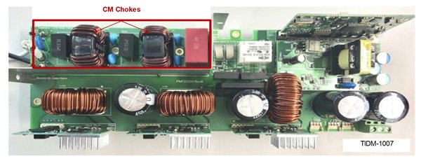
With advances in passive components lagging behind high-speed power semiconductor devices as well as circuit topologies, the volume of the passive filter is one of the limiting factors for increasing power density. Practical filter implementations can occupy as much as 30% of the total volume of a power solution, as shown in Figure 1.


Figure 1: A conventional single-phase passive EMI filter in a 3.3-kW totem-pole power factor correction reference design


Reduce system size, weight and cost 

 Learn more about our power-supply filter ICs.

Active EMI filter (AEF) circuits enable more compact filter solutions for next-generation power-management systems. Space-constrained applications can use active power-supply filter integrated circuits (ICs) to reduce the size of magnetic components and the overall filter. Additional benefits of an AEF include lower component power losses for better thermal management and higher reliability, reduced coupling between components within a confined space, easier mechanical and packaging design, and lower costs.

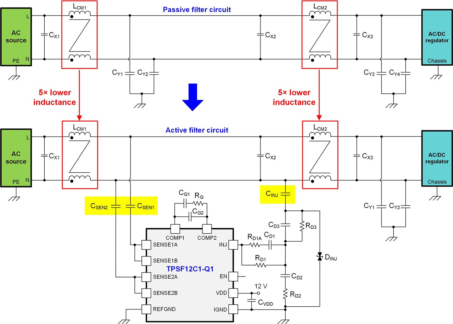
Figures 2 and 3 are schematics of single-phase and three-phase filter circuits, respectively, where an active solution replaces a traditional passive design. The single-phase TPSF12C1-Q1 and three-phase TPSF12C3-Q1 AEF ICs, positioned between the CM chokes, provide a lower-impedance shunt path for CM currents. As illustrated, the active solution has CM chokes LCM1 and LCM2 with much lower inductance relative to the same components in the passive filter.


Figure 2: Single-phase passive EMI filter (top) and corresponding AEF circuit with lower CM choke inductances (bottom)


Figure 3: Three-phase passive EMI filter (top) and corresponding AEF circuit with lower CM choke inductances (bottom)

AEFs

With Y-rated sense and injection capacitors connected to the AC lines, the circuits aim to reduce the total filter volume yet maintain low values of the line-frequency leakage current to chassis ground. This is possible by using an active circuit that shapes the frequency response of the injection capacitor – effectively increasing its value for high frequencies. In turn, the amplified injection capacitance over the frequency range of interest for EMI mitigation will lower CM choke inductances relative to the values of a passive filter with comparable attenuation.

The circuit advantages using an AEF are:

  • A simpler filter structure with a wide operating frequency range and high stability margins (calculated using the common-mode AEF quickstart calculator tool).
  • A reduced CM choke size with lower volume, weight and cost. This also enables much lower copper losses and better high-frequency attenuation performance from reduced choke self-parasitics.
  • No additional magnetic components – the AEF circuit only uses Y-rated sense and injection capacitors, with no impact to peak touch current during a fault condition.
  • Enhanced safety using a low-voltage AEF IC referenced to chassis ground.
  • A stand-alone IC implementation that offers flexibility in terms of placement near the filter components.
  • Immunity to line voltage surges to help meet International Electrotechnical Commission 61000-4-5.

The X-capacitor(s) placed between the two CM chokes in Figures 2 and 3 provide a low-impedance path between the power lines from a CM standpoint, typically up to low-megahertz frequencies. This allows current injection onto one power line, usually neutral, using only one injection capacitor. If the three-phase filter is a three-wire system without a neutral, the SENSE4 pin of the TPSF12C3-Q1 ties to ground and the injection capacitor couples through a starpoint connection of the X-capacitors.

Practical AEF implementation

Figure 4 shows a practical AEF implementation suitable for the converter in Figure 1. Using the TPSF12C1-Q1 single-phase AEF IC achieves CM noise attenuation.


Figure 4: Single-phase filter evaluation board with the AEF rated at 10 A

Figure 5 shows EMI results with the AEF disabled and enabled.


Figure 5: European Standard 55032 Class B EMI results with the AEF disabled and enabled

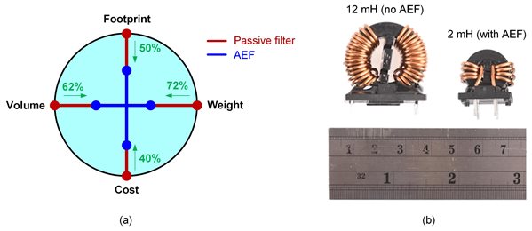
As evident in Figure 5, an AEF provides up to 30 dB of CM noise attenuation in the low-frequency range (100 kHz to 3 MHz), which enables a filter using two 2-mH nanocrystalline chokes to achieve CM attenuation performance equivalent to a passive filter design with two 12-mH chokes. To make a fair comparison, these chokes come from the same component family (made by Würth Elektronik) with a similar core material. Table 1 captures the applicable CM-choke parameters for the passive and active designs, and Figure 6 highlights the volume, footprint, weight and cost savings.


Filter design

CM choke part number

Qty

LCM1, LCM2 

(mH)

RDCR(mΩ)

Size 

(L × W × H, mm)

Total mass (g)

Total power loss 

(W) at 10 A, 25°C

Passive

7448051012

2

12

15

23 × 34 × 33

72

6.0

Active

7448031002

2

2

6

17 × 23 × 25

20

2.4

Table 1: CM choke parameters for the passive and active filter solutions

Figure 6: Footprint, volume, weight and cost reductions enabled by an AEF (a); choke size comparison (b)


The AEF in this example achieves a 60% total copper loss reduction at 10 A (neglecting the winding resistance increase from the temperature rise), which implies lower component operating temperatures and improved reliability.

Conclusion

It’s challenging to achieve a compact and efficient design for the EMI filter stage in high-density switching regulators, particularly for automotive and industrial applications where solution size and cost are such priorities. Practical results from an active filter solution to suppress the measured CM noise signature indicate a significant volumetric reduction of the CM choke components when benchmarked against an equivalent passive-only filter design.

Additional resources:

Addressing 3 power design challenges for corner radar systems

$
0
0
Other Parts Discussed in Post: LP87745-Q1, AWR2944

Co-authored by Abby Kainer

In the past decade, radar-sensing technology began replacing traditional automotive-sensing modalities given its many advantages – which include long-range detection, higher resolution and increased accuracy – for the implementation of driver safety features, autonomous driving and advanced driver assistance systems.

Radar technology directly measures the distance and radial velocity of oncoming objects in any weather condition, including heavy rain, snow and bright sunlight, thus making it a good technology for meeting New Car Assessment Program requirements. As an effect of the increasing automotive radar market, corner radar technology has quickly evolved.

Corner radars, placed at the two front corners and two rear corners on a vehicle, sense output object data sent over low-bandwidth networks such as Controller Area Network-Flexible Data Rate (CAN-FD) for the radar to process directly. Corner radars aid in applications such as lane-change and cross-traffic assistance, blind-spot detection, collision avoidance, pedestrian detection, and distance warnings.

Designing a reliable corner radar application can be challenging, however, especially when designing the power supply, since radar sensors typically require specific noise and ripple levels, power capabilities, and thermal dissipation to avoid affecting radio-frequency (RF) performance.

As we see it, there are three power-supply design challenges for corner radar applications:

  • The size of the power supply. A physically smaller power supply provides greater power density and efficiency, offering you additional flexibility to add more components to your design. Smart corner radar applications need a smaller solution size given the limited space available in the corners of a vehicle. A smaller power-supply size will also reduce overall system costs while providing the same amount of power.
  • The low ripple and noise specifications of radar sensors. Ripple directly impacts the output voltage accuracy and noise level of the power supply, which in turn affects the system’s overall RF. You could use second-stage inductor-capacitor (LC) filters or low-noise low-dropout regulators (LDOs) to help suppress noise spurs and ripple, but these components typically compromise the power supply’s size, temperature and overall cost.
  • The temperature of the power supply. As radar power supplies get smaller, the heat generated per unit area increases. High temperatures can compromise the integrity and life span of the power supply. If the radar chip overheats, the speed of its operation can slow down or, in extreme cases, shut down the entire system. For smart corner radars specifically, high temperatures compromise the radar’s ability to measure the distance and radial velocity of oncoming objects.

How a PMIC can help resolve power-supply challenges

Power-management integrated circuits (PMICs) can address the challenge of achieving power density with a reduced solution size and simplified power architecture when compared to a discrete implementation. PMICs that have built-in sequencing can help monitor temperature levels and meet all Automotive Safety Integrity Levels.

One approach is to use a combination of three low-noise buck converters and a 5-V boost converter PMIC for radar monolithic microwave ICs. The LP87745-Q1a small-size PMIC designed for radar sensors.

The DC/DC switching of the LP87745-Q1 helps reduce overall cost, reduces noise spurs, lowers ripple amplitude and enables a switching frequency (fsw) of 17.6 MHz, which provides two main benefits:

  • You can eliminate the second-stage LC filter on each supply rail. Because the high fsw is greater than radar technology’s intermediate frequency, there is no need for the filters.
  • A high fsw creates a lower ripple amplitude and reduces noise spurs, while making it easier to control noise levels.

With the elimination of the external LC filters and LDOs, the LP87745-Q1 will have lower levels of thermal dissipation that will not affect the RF performance of the radar chipset. The temperature levels of the LP87745-Q1 manage the thermal dissipation levels of the power supply, preserving the integrity of the radar chip.

As illustrated in Figure 1, the LP87745-Q1 supports a 5-V rail for CAN-FD-based radar chipsets such as the AWR2944.

Figure 1: The LP87745-Q1 powering the AWR2944 radar chip for corner radar applications

Conclusion

It is important to address power-supply challenges in order to have the most efficient radar application, and to protect drivers and passengers. The LP87745-Q1 helps support ASIL C functional safety systems; the elimination of additional voltage monitors helps make it easier to meet functional safety requirements at a system level. The LP87745-Q1’s novel feature set helps solve power-supply design challenges for corner radars, with the potential for use in front, in-cabin and cascaded radar designs.

Additional resources

Decrease factory downtime in 24-VDC power distribution with advanced load diagnostics

$
0
0
Other Parts Discussed in Post: TPS274C65

In Industry 4.0, the amount of diagnostic data is growing each year, enabling systems to become smarter, remain online longer and – in the end – increase productivity. In programmable logic controller (PLC) systems, robotics and machine tools, one area that is still traditionally lacking diagnostic data is 24-VDC power, which distributes power to different control systems in a factory.

If something goes wrong with 24-VDC power distribution, the lack of load diagnostic data often requires long debugging checklists full of rudimentary steps (such as “Is the power-good LED green or red?”) or intrusive investigations such as module disassembly, which increases downtime and decreases productivity.

Current sensing is a load diagnostic that when added to a 24-VDC power distribution network improves data collection, making it possible to diagnose overload currents, wire breaks and aging mechanical systems, or identify whether a load turned on correctly or not all.

The ability to sense current with an analog-to-digital converter (ADC) and a current-sense amplifier or high-side switch with integrated current monitoring has always been available. However, given factors such as isolation barriers, the limited number of ADC channels, or the routing of ADC channels, the implementation of current sensing can be expensive or difficult. 

One way to add current sensing while not overcomplicating a system would be to use a high-side switch with an integrated ADC. The TPS274C65 packs four 65-mΩ high-side switches into a 6-mm-by-6-mm quad flat no-lead package which leads to a reduction in power dissipation of 38% versus similar industrial high-side switches available in the market. The high-side switch channels and ADC are controllable and configurable through Serial Protocol Interface communication. Integrating the current-sense circuitry and ADC in the TPS274C65 enables it to transfer current-sense data over isolation barriers in digital output modules and reduce the routing of ADC channels, since all of the routing occurs inside the chip. Additionally, the device can also sense the temperature of the internal metal-oxide semiconductor field-effect transistors (MOSFETs) and sense voltage on the input and outputs.

Figure 1 is a block diagram illustrating how the TPS274C65 in a digital output module helps increase the amount of data sent back to the PLC controller over the isolation barrier.


Figure 1: The TPS274C65 in a digital output module application

Let’s focus now on the TPS274C65’s use in factory applications such digital outputs; remote input/output (I/O) modules; and larger systems such as robots, computer numerical control machines and multicarrier systems. 

Using current sensing to shorten debugging checklists

As I mentioned above, without diagnostic data, repairing systems can lead to long debugging checklists or intrusive investigations such as module disassembly. This can be problematic for complex systems such as robots and machine tools. The integrated ADC in the TPS274C65 enables both on-site and remote checks to determine the correct distribution of power to the different sensors, relays and subsystems, which helps eliminate potential root causes and enables users to identify problems more quickly. Such monitoring also lets users know if a subsystem is not working properly – for example, they could bring a spare part if on-site debugging is required.

Figure 2 shows what a command center for a power-distribution network could look like in a digital output, remote I/O, machine or robot application. This level of detail could help provide more information to help find the root cause of an offline system.


Figure 2: The TPS274C65USB evaluation module GUI


Using current sensing to provide predictive maintenance and predictive resolution

To take it one step further, having diagnostic data that shows how a system had been operating before it failed enables the establishment of a predictive resolution procedure to prevent future machines from failing in the same way. For instance, using current sensing to determine whether a small motor or actuator is drawing more current to perform the same function could mean that it is aging, close to failure, or that some mechanism might need servicing. 

The integrated ADC in the TPS274C65 enables the collection of this data to perform predictive maintenance and predictive resolution, thus making sure that downtime is planned rather than unplanned. For example, capturing the load-current profile of a solenoid valve could detect whether the valve performance is changing over time. Does the valve have any additional life, or does it need replacing?

Figure 3 shows how the integrated ADC senses the load-current profile of the solenoid valve.


(a)

(b)

Figure 3: Example of the current-sensing capability of the TPS274C65: a scope shot showing the load-current profile of a solenoid valve (a); a readout from the TPS274C65 ADC of the load-current profile of a solenoid valve (b) 

Conclusion

The TPS274C65’s current-sensing capabilities in factory automation systems decrease downtime and increase productivity. In the end, it will really come down to how you can use this tool in your toolbox to make power distribution smarter.

Additional resources

How can you optimize SWaP for next-generation satellites with electronic power systems?

$
0
0
Other Parts Discussed in Post: TPS7H5001-SP

In the satellite industry, dramatic increases in local data processing, support for higher throughput communication links and the rapid adoption of electrical propulsion systems are driving demand for much higher performance electrical power systems (EPSs). The EPS is part of the bus section of a satellite, providing structural support and housing subsystems such as power, thermal management, communication and propulsion. The EPS generates, stores, regulates and distributes power to all other subsystems and payloads onboard the satellite.

The unique challenges and constraints of space missions require optimizing size, weight and power (SWaP). Here are some of the reasons why SWaP is such a big deal in satellite designs:

  • Mission requirements: Requirements such as data transmission rate, resolution and sensitivity can impact a satellite’s SWaP requirements.
  • Launch limitations: Satellites have size constraints, weight constraints and cost-of-launch constraints that can be $10,00 to $1000,00 per kilogram based on the intended orbit.
  • Power generation: Satellites generally rely on solar panels, and the size and weight of the panels limit the amount of generated power. The power-generation capacity also affects the weight and size of components, like batteries, and functions such as power distribution and thermal management.
  • Operational efficiency: SWaP optimization enables satellites to operate more efficiently in space, resulting in better performance and longer mission lifetimes.

Because power is one of the most valuable resources on a satellite, maximizing EPS efficiency can help extend mission lifetimes, reduce mass and volume, and minimize thermal management overhead.

Beyond efficiency, an EPS must also handle a wide range of voltages and currents because of the number of power-supply topologies. Figure 1 shows some of the most common topologies.

Figure 1: Common power-supply topologies in satellite power architectures

The components and functions, shown in Figure 2, of a typical satellite EPS are:

  • Solar panels (or energy generation): Solar panels are the primary power source for most satellites.
  • A battery (or energy storage): The battery stores excess power generated by the solar panels during daylight hours, and provides power to the satellite during an eclipse or when the solar panels are not generating enough power.
  • Power-conditioning unit (PCU): The PCU regulates the electrical output of the solar panels and battery to provide a stable and consistent voltage and current to the rest of the satellite.
  • Power-distribution unit (PDU): The PDU distributes power generated by the solar panels and battery to the various subsystems and payloads onboard the satellite.
  • Backup power supply: If the primary EPS fails, a backup power supply will help maintain the most essential functions until the restoration of the primary system.

Figure 2: A typical satellite EPS

One way to optimize the SWaP design challenge in these types of systems is to use pulse-width modulation (PWM) controllers. For example, the radiation-hardened TPS7H5001-SP(100 krad TID, 75 MeV⋅cm2/mg) and radiation-tolerant TPS7H5005-SEP (rad-tolerant 30 to 50 krad TID, 43 MeV⋅cm2/mg) controller families enable the use of a common power architecture for many of the circuits in an EPS across a number of different missions and diverse orbits.

To help engineers optimize the SWaP in their satellite power system, the following reference designs use space-grade space-grade PWM controllers in various power-supply circuits across the satellite, not only in the EPS, but also on select payload boards:

  • Isolated flyback design:
    • A 100-W isolated synchronous flyback topology that supports an input of 22 V to 36 V with an output of 5 V and uses GaN FETs in the power stage.
    • This design is optimized for power-supply topologies that require only a single output.
  • Non-isolated high-current dual-phase buck design:
    • This design uses the TPS7H5001-SP controller in a single-phase synchronous buck topology supporting an input of 11 V to 14 V with an output of 1 V and uses GaN FETs in the power stage. The design is capable of supporting 20 A and maintains tight DC and AC tolerance.
    • You can extend this design to a multiphase solution optimized for payload designs that require high current (>50 A) and low input voltages (sub-1 V) to power the core rails of some advanced field-programmable gate arrays and multicore central processing units.

Conclusion

With power being one of the most valuable resources on a satellite, the EPS architecture can have a significant impact on the overall design. TI’s radiation-validated PWM controller families provide high efficiency and support a wide range of topologies, as well as an architecture that’s deployable in a diverse set of missions and orbits.

Additional resources


How to deliver current beyond 100 A to an ADAS processor

$
0
0
Other Parts Discussed in Post: TDA4VH-Q1, TPS62876-Q1

This article was co-authored by Tanvee Pandya and Goeswami Deva Singh.

The electrification of vehicle systems is growing in advanced driver assistance systems (ADAS), which include vision analytics for autonomous driving, parking assistance and adaptive control functions. Smart connectivity, safety-critical software applications, and neural network processing all require enhanced computing power in real time.

Meeting these advanced needs requires a multicore processor such as the TDA4VH-Q1, which can support electronic control units (ECUs) beyond 100 A. But the design challenges associated with high power include achieving efficiency for higher current rails, controlling thermal performance and load transients at full loads, and meeting functional safety requirements.

Delivering ADAS processing power

The TPS62876-Q1 buck converter helps designers address currents beyond 30 A with a novel stackability feature that achieves the high currents necessary to power a system-on-a-chip (SoC) such as the TDA4VH-Q1. The family includes devices ranging from 15 A to 30 A, available in the same package, and Stack feature that can support to reach load current beyond 100A.

Stacking these devices not only helps power the core of next-generation ADAS SoCs, but also helps improve thermal performance by reducing thermal limitations, and increase efficiency. See Figure 1.


Figure 1: Two TPS62876-Q1 devices in a stacked configuration

Stacking operates by using the daisy-chain method. The primary device controls one compensation network, one POWERGOOD pin, one ENABLE pin and one I2C interface. For optimal current sharing, you must program all devices in the stack to use same current rating, the same switching frequency and the same current level.

The primary device in the stack also sets the output voltage and controls its regulation. If there is a 47-kΩ resistor between the SYNCOUT pin and ground, the device operates as a secondary device. If the SYNCOUT pin is high impedance, the device operates as a primary device. Figure 2 shows the stack configuration implemented on a printed circuit board.

Figure 2: Example evaluation module of three stacked TPS62876-Q1 buck converter

Other features in this family of buck converters include:

  • Droop compensation, also known as load line (automatic voltage positioning). Scaling the nominal output voltage provides better load-transient tolerance based on the output current (15 A to 30 A) and helps reduce the output capacitance, enabling a cost-optimized, high-power-density solution. The REGISTER pin enables or disables droop compensation, which is disabled by default.
  • Remote sensing supports a wider range of SoC processors with a tighter output-voltage requirement that provides more headroom during load transients. The device’s remote sense lines connect directly to the point of load, which allows you to set the voltage with an accuracy of 0.8%.
  • The I2C interface monitors system performance and sends a warning if the temperature and output current exceed specified limits. It is also possible to use dynamic voltage scaling to adjust the output voltage from 0.4 V to 1.675 V. If you do not need the I2C feature, you can still use same device by connecting the SCL and SDA pins to ground.

Functional safety

Functional safety is an important aspect in ADAS, especially when it comes to autonomous driving. The TPS62876-Q1 buck converter offers TI Functional Safety-Capable levels of documentation, which include:

  • The functional safety failure-in-time rates of the semiconductor component estimated by the application of industry reliability standards.
  • Component failure modes and their distribution based on the device’s primary function.
  • Pin failure-mode analysis.

Adding an external supervisor to your design enables you to achieve Automotive Safety Integrity Level standards.

Conclusion

Moving toward higher autonomy levels such as Society of Automotive Engineers Level 2 will require more computational capabilities to provide higher resolutions and quick responses in a very short time. Embedding features such as artificial intelligence technologies also increases the need for more power-hungry ADAS SoC processors. The stackability of the TPS62876-Q1 family helps you achieve core power beyond 100 A to enable a higher level of autonomous driving.

Additional resources

How to enhance power and signal integrity with low-noise and low-ripple design techniques

$
0
0
Other Parts Discussed in Post: TPSM82912, TPS7A94, TPSM82913, TPS62913, TPS62912

Improving accuracy and precision, and minimizing system noise is a common challenge for engineers designing a power supply for noise-sensitive systems for medical applications, test and measurement, and wireless infrastructure that use clocks, data converters or amplifiers. Although the term “noise” can mean different things to different people, in this article I’ll define noise as low-frequency thermal noise generated by resistors and transistors in the circuit.  You can identify noise through a spectral noise-density curve in microvolts per square-root hertz, and as integrated output noise in root-mean-square microvolts, typically over a specific range from 10 Hz to 100 kHz. Noise in the power supply can degrade the analog-to-digital converter’s performance and introduce clock jitter.

The traditional setup for powering a clock, data converter or amplifier is to use a DC/DC converter (or module), followed by a low-dropout regulator (LDO) such as the TPS7A94, TPS7A82, TPS7A84TPS7A52TPS7A53 or TPS7A54, followed by a ferrite-bead filter, as shown in Figure 1. This design approach minimizes both noise and ripple from the power supply and works well for load currents below approximately 2 A. As loads increase, however, the power loss in the LDO introduces issues in efficiency and thermal management; for example, a post-regulation LDO can add 1.5 W of power loss in a typical analog front-end application. Are those of you looking for low noise and efficiency in your design out of options? Not quite.

Figure 1: A typical low-noise architecture using a DC/DC converter, LDO and ferrite-bead filter

Using a low-noise buck converter or module in place of an LDO

One way to keep the power loss in check is to minimize the dropout through the LDO. However, this approach will have a negative impact on noise performance. Additionally, higher-current LDOs are typically larger, which can increase design footprints and cost. A more effective way to ensure low noise while controlling the power loss is to eliminate the LDO from the design altogether and use a low-noise DC/DC buck converter or module, as shown in Figure 2.

Figure 2: Using a low-noise buck converter without an LDO

I know what you’re thinking: How does removing the primary device that reduces noise still provide a low-noise supply? Many LDOs have a low-pass filter on the bandgap reference to minimize the noise into the error amplifier. The TPS62912 and TPS62913 family of low-noise buck converters, as well as the TPSM82912 and TPSM82913 modules, implement a noise-reduction/soft-start pin for connecting a capacitor, forming a low-pass resistor-capacitor filter using the integrated Rand externally connected CNR/SS, as shown in Figure 3. This implementation essentially mimics the behavior of the bandgap low-pass filter in an LDO. If you still need lower noise than the TPS62913 or TPSM82913 can provide, you can use a low noise LDO like the TPS7A94 with a reduced dropout, lower power dissipation, and still achieve extremely low noise.  This is explained in more detail in App Brief SBVA099.

Figure 3: Low-noise buck block diagram with bandgap noise filtering

What about the output voltage ripple?

Every DC/DC converter generates an output voltage ripple at its switching frequency. Noise-sensitive analog rails in precision systems need the lowest supply voltage ripple to minimize frequency spurs in the spectrum, which typically depend on the switching frequency of the DC/DC converter, inductor value, output capacitance, equivalent series resistance and equivalent series inductance. To mitigate the ripple from these components, engineers often use an LDO and/or a small ferrite bead and capacitors to create a pi filter to minimize ripple at the load. A low-ripple buck converter such as the TPS62912 and TPS62913, as well as the TPSM82913 module, leverage this ferrite-bead filter by integrating ferrite-bead compensation and remote-sense feedback. Using the inductance of the ferrite bead in combination with an additional output capacitor removes the high-frequency components in the output voltage ripple and reduces the ripple by approximately 30 dB, as shown in Figure 4. 

Figure 4: Output voltage ripple before the ferrite-bead filter (a); and after the ferrite-bead filter (b)

Conclusion

By integrating features that mitigate system noise and ripple, low-noise buck converters can help engineers achieve a low-noise power-supply solution without the need for an LDO. Of course, the noise levels required by different applications will vary, as will the performance for different output voltages, so only you can determine the best low-noise architecture for your design. But if you’re looking to simplify the design of noise-sensitive analog power supplies, reduce power losses, and shrink the overall design footprint, consider using a low-noise buck converter.

Additional resources

How to design wearables that are smaller and go longer between charges

$
0
0

Earlier this year, I wrote about wearables and how they can do so much and be so small. Well, wearable devices are about to get smaller, do more and last longer thanks to innovations in battery charging, low quiescent current operation, smart power management and high integration.

Battery charging for wearables is challenging because you have to use batteries that are both small in size and capacity. For example, charge currents vary greatly depending if you are using a 40 mAh, 100 mAh or 200 mAh battery, and whether you want to charge at 0.5 C, 1 C or 2 C to achieve fast charge and charge cycle life goals. The key is to include a programmable fast charge current into your design. The bq25120 battery management solution offers programming from 5 mA up to 300 mA to support a wide variety of batteries and charging profiles.

While it is important to charge quickly, it is also important to get as much energy into the battery as possible. To do this, the termination current must be very accurate and have the ability to terminate reliably at 1 mA or below.

The battery must power the microprocessor (MCU), radio and sensors between charges. To maximize battery life, you need to focus on components that can consume low power when operating, as well as consume very low power when shut down. The buck converter is the most important feature for low Iq operation, since it is the power supply to the MCU and must be operating at all times. Consider implementing a product that integrates a very low current DC/DC converter such as the bq25120. This product enables 700 nA Iq while the 1.8 V rail is on and powering the MCU at no load. If your wearable needs an additional low Iq buck, the TPS62743 or TPS62843 is a great choice. TPS62843 is the new generation of ultra-low-IQ buck converter. With operating quiescent current 275-nA typical, the device extends a high efficiency at light-load down to 100-μA and below. It is optimized for 1uH inductor and down to 4.7 uF Cout. With the tiny 6-pin WCSP package (0.8 mm x 1.05 mm) and small passive components it supports a total solution size down to 5.7 mm². The wide output voltage range (0.4 V – 3.6 V) and 600 mA output current make the device fit for most of battery powered applications, such as wearable electronics, earbuds, TWS, medical sensors, hearing aids and IoT. 

Some sensors and radios are not used all the time and can be shut down completely, requiring so a low leakage shutdown mode is needed. The bq25120 integrates a load switch that can turn off components when not used, and can also be configured as a regulated LDO output if needed.

Some wearables have displays or heart rate monitors (HRMs) that require boost converters. Different displays have different voltage requirements, so the most flexible solution is to implement the boost with discrete devices. If the display is an organic light emitting diode (OLED), consider a device like the TPS61046 , which provides the 12-V and is small with low Iq. If the display is an LCD, E Ink display or a Heart Rate Monitor (HRM), the TPS61240 is ideal for providing the 5V. HRMs require a 5V supply for the LEDs, and the TPS61240 has a very low leakage disconnect switch for turning them off completely when not in use.

As you can see, TI has a variety of small, power-efficient components to create wearable devices that really stand out in today’s market. Here’s to living healthier with TI technology.

Additional resources

Extending battery life with a boost converter

$
0
0
Other Parts Discussed in Post: TPS61299

Eileen Zhang co-authored this technical article

A device’s quiescent current, or IQ, is an important parameter for low-power, energy-efficient end equipment such as continuous blood glucose monitors (CGMs). The current drawn by the integrated circuit at light or no loads significantly influences power losses in standby mode and the total run time of the system.

The load powered by the battery is not actually always on but is a pulse-width modulation (PWM) load, meaning that the load is made up of two periods: tPWM and tStandby, shown in Figure 1. While tStandby takes up 99.9% of the total load cycle, denoted as T in Figure 1, it is still important to improve efficiency, especially light-load efficiency.


Figure 1: Load condition of a battery system

The challenge is to decrease power losses in standby mode and to limit current spikes and decrease the duty cycle during the on-pulse period, thus enhancing efficiency and extending battery life. A boost converter with low IQ can help cut down the total power losses for a battery.


Choose a low-IQ boost converter to enhance overall efficiency

A CGM shows why it’s important to minimize IQ to extend battery life. Figure 2 shows a CGM power block: a sensor to read the glucose concentration, a transmitter to capture the glucose reading, and a wireless receiver for communication and display. The transmitter, consisting of a coin-cell battery, boost converter and analog front end (Figure 3) consumes the most power.


Figure 2: Power architecture of a CGM


Figure 3: Power architecture of a CGM transmitter

 Figure 4 shows the load current of the analog front end. As you can see, the transmitter is in standby mode 99% of the time.


Figure 4: Current consumption vs. time in a CGM transmitter

 Equation 1 calculates the total power supplied by the battery during one load cycle as:


Lowering the IQ could directly improve efficiency in standby mode.

TI’s TPS61299 boost converter only consumes 95 nA of IQ from VOUT, making it possible to increase efficiency 39% under the typical standby conditions of a CGM: VIN = 3.0 V, VOUT = 3.3 V and standby IOUT = 10 µA (Figure 5). An on-pulse load of 30 mA lasting 600 ms every 288-s load cycle translates to as much as 2.53 W of power saved per day. This efficiency increase in standby mode can ultimately lengthen battery life by 20%.


Figure 5: Efficiency curve of the TPS61299 and a 600-nA IQ device


Limit the discharge current from the battery

Although high-energy-density, low-discharge coin-cell batteries are extremely popular, their main drawback is a high equivalent series resistance (ESR) and limited current capability. For a PWM load application, the duty cycle is small, and high current pulses add to the high inrush current spikes, which are much higher than the discharge current and have detrimental effects on battery capacity and battery life – especially when using a supercapacitor. Also, as the battery ages, the ESR increases, and the power loss caused by current spikes increases accordingly.

Battery capacity is inverse with discharge current, and battery life is linear with capacity, as shown in Figure 6. Decreasing the discharge current from 500 mA to 100 mA doubles the battery life.

The TPS61299 boost converter family, available in input current limits from 5 mA to 1.5 A, accurately limits discharge current during the on-pulse period, helping prolong battery life.


Figure 6: Battery life vs. discharge current


Select a device with fast transient response times

Decreasing the on-pulse width of the load to decrease the total power loss also extends overall battery life.

Figure 7 illustrates the load condition cycle-by-cycle of a smartwatch LED. The PWM load covers two stages: transient time (ttran) and sampling time (tsample). ttran measures how fast the boost converter regulates back to the targeted output voltage after an abrupt change in load current or supply voltage. tsample is a constant value once the photodiode settles.

Shortening ttran can largely narrow the PWM time (tPWM), widening the blanking time (tBLANK) in turn and enabling a longer low-IQ working state. Assuming that it is possible to decrease ttran from 100 µs to 10 µs, with a 10-µs tsample the cycle time is 250 µs, enabling an extension of tBLANK from 140 µs to 230 µs, as shown in Figure 8.


Figure 7: Traditional PWM load


Figure 8: PWM load with fast transient performance

It is always a struggle to maintain low IQ to achieve high efficiency during tBLANK and a shortening ttran . Low-IQ devices always suffer from longer response times because it is challenging to recharge the internal parasitic capacitors with very low IQ.

Nevertheless, the TPS61299 can achieve faster transient response times with a wider bandwidth. For example, as shown in Figure 9, the typical settling time with an output-current step up from 0 mA to 200 mA under 3.6-V input and 5-V output conditions is 8 µs.

Figure 9: Transient waveform of the TPS61299 

Conclusion

The TPS61299 boost converter simultaneously integrates three of the most effective ways for designers to reduce total battery power losses:

  • Choose a low-IQ boost converter to enhance overall efficiency.
  • Limit the discharge current from the battery.
  • Select a device with fast transient response time.

Above all, higher efficiency and lower power losses for boost converters will continue to be trends in battery applications, while lower RDS(on) and an optimized control loop may also contribute to lengthening battery life.


Additional resources

  • Download the application note, “Advantages of the TPS61299 with Fast Transient Performance in Smartwatch Applications.”

Addressing design challenges with user-programmable power-management integrated circuits

$
0
0
Other Parts Discussed in Post: TPS6521905

Jad Panjaitan co-authored this technical article

Advancements in processor and field-programmable gate array (FPGA) technology are complicating power requirements. In addition to supplying the correct voltages and currents to power rails, many power solutions need features such as power sequencing (the activation of power rails in a certain order), low-power modes and monitoring elements.

While it is possible to build a solution using discrete parts, power-management integrated circuits (PMICs) can accelerate the design process. PMICs unify many common power-management functions into a single energy-efficient chip, which can simplify designs and shrink power solution sizes.

Advantages of user-programmable PMICs

There are many types of PMICs: factory-programmed, hardware-configurable and software-configurable. But in situations where wide flexibility and easy customization are high priorities, a user-programmable PMIC can be a better fit, giving impressive control over details such as power rail voltages and power sequencing. Linux® drivers developed specifically for these PMICs enable the system to trigger reboots, soft restarts and low-power modes; they also enable dynamic voltage scaling, adapting buck-converter voltages to match the system’s current power needs.

It is common for a system’s power requirements to change during the design process. You might add or remove peripheral parts, upgrade or swap processors, or want different power modes.

A good example would be the FPGA. The reconfigurability of the FPGA is one of its strongest selling points, but any change to its design and dynamic load requirements will also affect its power-management requirements.

When it comes to customization, the other kinds of PMICs have limitations. For example:

  • Factory-programmed PMICs are catalog or custom devices that are pre-programmed to power specific processors or FPGAs, and require a large-volume business case.
  • Hardware-configurable PMICs use resistors to change the output voltages, which may lead to power solutions with a larger printed circuit board footprint. Also, adding power sequencing will then require an external sequencer or microcontroller.
  • Software-configurable PMICs need an accompanying microcontroller to configure them at startup; these configuration changes are not permanent, and the PMIC must be reconfigured after each power cycle.

Any category of PMIC can offer some level of adjustment to these changing requirements, but the customizability of a user-programmable PMIC is a solid complement to the adaptability of the FPGA; user-programmable PMICs can reduce the amount of time revising FPGA power architectures without compromising the quality of power solutions, giving you more flexibility to experiment with different FPGA designs.

It is possible to reprogram a user-programmable PMIC such as the TPS6521905 multiple times through its electrically erasable programmable read-only memory (EEPROM). The TPS6521905 is initialized with a blank EEPROM, disabling all power rails until configuration and avoiding any potential damage during the production process if you will be powering and placing the PMIC into the prototype board before reprogramming.

Figure 1 is a block diagram of the TPS6521905.

Figure 1: Block diagram of the TPS6521905

Using I2C communication, you can program the three buck converters and four low-dropout regulators of the TPS6521905 to customize power rail voltages and power sequences and toggle different operating modes. You can set safety features such as undervoltage sensing and temperature thresholds, and configure the three multifunction pins and three digital input/output pins to interface with other devices. If the system needs more power rails, then you can synchronize multiple TPS6521905 devices, as illustrated in Figure 2.

Figure 2: Cascading multiple TPS6521905 devices

The TPS6521905 comes in a package size as small as 4 mm by 4 mm, and operates at a switching frequency of 2.3 MHz; the compact sizing and high switching frequency allow for smaller input/output inductance and capacitance requirements, which can save space and lower system costs.

Prototyping to production

A user-programmable PMIC is a blank slate with many customization options. It can reduce design cost and time, and is often reusable across different projects. It is possible to reprogram a single part number to substitute several for different part numbers, simplifying the supply chain.

Let’s go through the steps of the prototyping-to-production process with a user-programmable PMIC such as the TPS6521905:

  1. Define the specifications of the nonvolatile memory settings according to your power solution requirements.
  2. Reprogram the TPS6521905 with the TPS65219-GUI and TPS65219EVM-SKT, using the programming guide and tutorial video as references.
  3. Perform testing and validation on the configured PMIC, reevaluating the design until it satisfies your system requirements.
  4. Once you have finalized the design, export the custom TPS65219-GUI register settings.
  5. Your company can mass-program the TPS6521905 registers independently or use a third-party programming service.

Conclusion

A user-programmable PMIC can be a good choice given its many customization options; it can also accelerate design processes and reduce system costs while maintaining power efficiency and compact sizing.

Working with user-programmable PMICs can be a new experience for engineers. TI aims to ease the process and offer technical support at every step of the way through user-programmable PMIC user guides, tutorial videos and application notes, as well as the TI E2E  design support forums.

Additional resources

Designing an application to support a wide input voltage and battery voltage

$
0
0
Other Parts Discussed in Post: BQ25756

It can be challenging for engineers to design applications using rechargeable batteries that provide the best charging experience for consumers when different projects have different battery-charging needs. Using a different battery charger for every application increases design time because you have to redesign, debug and requalify every new circuit.

What if you could minimize development time by selecting a battery charger that worked for a variety of projects? A single battery-charger integrated circuit (IC) with wide voltage input (VIN) and voltage output (VOUT) capability can help reduce development time by enabling you to use the same charger across a variety of applications with different input adapters and battery configurations. 

In addition to helping reduce design time, using a wide VIN and VOUT charger helps you explore new technologies such as solar and bidirectional charging, which can improve the charging experience for consumers. In this article, I’ll discuss the benefits of a wide VIN and VOUT buck-boost battery charger.


Supporting multiple designs using a single battery charger IC

Designing a battery-charging system for e-bikes is one application example that would benefit from using the same battery-charger IC across models. There is a new USB Power Delivery (PD) standard called Extended Power Range (EPR), with output power as high as 240W and VIN up to 48V. Because of the higher EPR power and convenience of using a standard USB Type-C® adapter, designers are looking to implement USB PD EPR charging for e-bikes, which requires the integration of a battery-charger IC into the e-bike battery pack.

E-bike companies have different models with different battery chemistries and charge voltages. Instead of using one battery charger to charge an e-bike with a 36-V battery and another battery charger to charge an e-bike with a 48-V battery, it would be more convenient to use the same battery charger for both models. Supporting the full voltage range of USB PD EPR adapters would also help minimize the amount of design changes necessary between models. To use the same battery charger, it must have a wide VIN to support the USB PD EPR input and a wide VOUT to support 36- to 48-V batteries.

Related to USB PD EPR, bidirectional charging is a new feature enabled by a wide VIN and VOUT battery charger. As shown in Figure 1, it is possible to charge a battery such as an e-bike battery when the battery charger is in forward mode and discharge the battery in reverse mode from the same USB Type-C port. This benefits consumers because the application has new functionality – being a power bank in addition to its usual operation. Supporting functionality as a power bank requires a battery charger with a wide VIN and VOUT and bidirectional charging in order to support the various input and output voltage combinations in forward and reverse mode.

Figure 1:Charging e-bike from USB (top) and charging personal device from e-bike (bottom)


Solar charging with different sunlight intensity

Solar panels offer a way for consumers to charge their products without grid-dependent outlets nearby. It is important to find the maximum power point (MPP) of the solar panels because their output serves as the input for the battery charger, as shown in Figure 2. A lower input power to the battery charger will have a lower charge current, resulting in longer charge times. A battery charger with a maximum-power-point tracking (MPPT) algorithm will autonomously find the MPP of the solar panel under different sunlight conditions. Using a wide VIN and VOUT buck-boost battery charger helps support the range of possible output-voltage values of the solar panel.


Figure 2: Solar charging block diagram

A portable power station would also benefit from a charger with an MPPT algorithm. For solar charging applications, designing the charging system using a battery charger with an autonomous MPPT algorithm helps fully harness the solar panel for shorter charge times.

Battery charger for wide VIN and VOUT

The BQ25756 buck-boost battery charger supports a 70-V operating voltage on the input and output and as much as 20 A of charge current, which meets the 240-W maximum USB PD EPR power levels. In addition to a wide VIN and VOUT range, the BQ25756 is also a bidirectional battery charger for charging and discharging through the same USB Type-C port. The device comes equipped with an advanced MPPT algorithm for solar charging, and can even find the MPPT with multiple solar panels connected in series or parallel with various sunlight conditions including partial shade. Using the wide VIN and VOUT, bidirectionality, and MPPT functionality of the BQ25756 enables its use across many designs.

Conclusion

Designing with a wide VIN and VOUT charger helps save engineers development time by reusing the same circuity across many applications.  Image you need to design a new portfolio of power tools.  Choosing a different battery charger for the drill, heat gun and blower can increase the work as you need to learn about three chargers.  Using the same charger across these power tools helps save the learning and development time compared to using multiple different chargers. 

In addition, wide VIN and VOUT chargers enable engineers to incorporate new technologies, such as USB Type-C  Power Delivery and solar charging.  Using a wide VIN and VOUT charger like BQ25756 with an MPPT algorithm helps engineers design products that can be charged anywhere with solar panels while providing the consumers with a fast charging experience.  Pairing BQ25756 with a TI USB-C PD Controller eliminates the hassle of having adapters that work for only one device.  With this pairing, consumers can leverage bi-directional charging and use a common USB-C adapter to charge many applications including power tools, e-bikes and portable power stations.  Wide VIN and VOUT chargers can improve the customer charging experience and reduce your development time.            

3 ways low-Iq technologies extend battery life without compromising system performance

$
0
0

With the world more battery-powered than ever, the demand for better and cheaper batteries and battery packs is soaring. And while battery manufacturers are introducing new chemistries and smaller packs, which are putting new and complex constraints on power requirements, the fundamental functionality remains the same: today’s batteries must have a maximized run time and an extended shelf life without compromising system performance.


Low standby power. Fast response time. Small form factor.

Learn more about the benefits of our low IQ technologies.

Minimizing quiescent current (IQ) is a priority when reducing power consumption, which in turn extends battery life. A device’s IQ is simply the current drawn, or power consumed, from the battery while in standby mode or light-load operation. IQ can significantly impact device efficiency, and in battery-powered applications, achieving high efficiency at no- or light-load conditions requires power-management solutions that tightly regulate the output while maintaining ultra-low supply current.

Many of today’s designs require mere nanoamperes of IQ, a feature that’s important for applications ranging from electric vehicles (EVs) all the way down to power tools, headsets, headphones and earbuds that require long standby operation. And because these types of systems spend more than 99% of their time in standby mode, the IQ in standby, or sleep, mode can be a limiting factor for battery life.

Optimizing power-management building blocks such as DC/DC converters, low-dropout regulators (LDOs), power switches, voltage references and supervisors, and battery-management devices can help enable low power consumption and extend battery life.

Here are the top three ways our low-IQ technologies can extend battery and shelf life without compromising performance.

Enabling low, always-on power

Ultra-low-leakage process technologies and novel control topologies enable long battery run times. Achieving ultra-low IQ when the system has gone into standby mode extends battery run time.

In Figure 1, the TPS37-Q1 supervisor achieves an IQ for EV battery monitoring at a typical 1 µA while still supporting up to 65-V supply voltages all without compromising on area or response time.


Figure 1: Direct 12-V/48-V off-battery voltage monitoring with TPS37-Q1


Battery-charger integrated circuits (ICs) such as the BQ25155 with an IQ of 10 nA in ship mode can help ensure that the battery does not get depleted, even when sitting for months or years on a shelf. Low-power regulators such as the TPS7A02 offer an ultra-low IQ of 25 nA and a ship mode with an IQ of 3 nA, helping increase battery life dramatically in normal and dropout operation.

Achieving fast response times

Fast wake-up comparators and zero-IQ feedback control enable fast dynamic responses without compromising low power consumption. Intelligent biasing schemes that instantaneously accelerate the comparator when there is an error detected improve speed without additional IQ. For example, in Figure 2, the TPS62843, a buck switching regulator with a typical 275-nA IQ, demonstrates a more than three times improvement in response time × IQ/ILOAD over previous generations. Additionally, the TPS37-Q1 has one of the best response and detection times in the industry (8 µs typically), which is at least two to 10 times faster compared to industry alternatives.


Figure 2: The TPS62843 load transient at 1.2 VOUT, IOUT_MIN = 0 A to IOUT_MAX = 300 mA


Reducing form factor

Area reduction techniques for resistors and capacitors facilitate integration into space-constrained applications while not affecting quiescent power. The next-generation nanopower devices eliminate the need for a majority of the external pullup and pulldown resistors and external resistor-divider networks, and offer much smaller form factors such as the TPS7A02 at a 640-µm-by-64-µm chip-scale package size.

Another way to save board area is to integrate more functions onto a single die. This integration enables blocks such as the supervisor, reference system, low-dropout regulator, battery charger and DC/DC converter to share common building blocks while reducing the combined IQ. The BQ25125, a battery-charger management IC available in a 2.5-mm-by-2.5-mm wafer chip-scale package, integrates and flexibly controls multiple low-IQ functions with I2C, which enables designers to bring an entire power-management system to multiple low-power applications.

Conclusion

With battery-powered applications becoming more ubiquitous, the increased demand for low IQ without compromising system performance can be daunting.  But it doesn’t have to be. At TI, our portfolio of ultra-low IQ technologies can help you achieve ultra-low power without trade-offs in performance and costs to maximize battery run time and extend shelf life in your next battery-powered designs.

Additional resources


Mitigating CMTI on a PSR flyback for SiC-based traction inverter designs

$
0
0

Kim Nielson co-authored this technical article

There has been a significant increase recently in the use of silicon carbide (SiC) field-effect transistors (FETs) in traction inverter designs. The fact that SiC inverters can produce high transient voltage (dv/dt) signals greater than 100 V/ns raises concerns for common-mode transient immunity (CMTI), representing a new challenge when designing an inverter gate driver isolated bias supply design.

Among isolated bias supply topologies, the primary-side regulated (PSR) flyback converter has the best cost-to-performance ratio given its low count of external components, tight output voltage regulation, no need for an optocoupler, high efficiency and reliable galvanic isolation. There is an effective CMTI mitigation method that can help improve PSR flyback immunity in a SiC inverter, enabling the PSR flyback’s continued use in SiC FETs and isolated bias supplies.

Using a PSR flyback as an isolated bias supply

Figure 1 shows the PSR flyback converter topology in traction inverter applications using TI’s LM5180 converter. PSR flyback devices such as the LM5181, LM25180, LM25183, LM25184 converters and the LM5185 controller, all share a common architecture with the LM5180; the main differences are in their power capabilities.

Figure 1 shows only two output rails biasing one high-side driver of the inverter’s SiC FETs. It is possible to add additional isolated outputs by coupling more windings to the transformer. The components represented dashed lines are optional for additional features.


Figure 1: PSR flyback bias supply for traction inverters


Unlike a conventional flyback converter, which typically requires an optocoupler and a voltage reference such as the TI TLV431 on the secondary side to form the feedback circuit for tight output regulation, the PSR flyback converter senses the output voltage through the transformer’s primary winding and achieves tight output voltage regulation of the isolated voltage rail, all without the need for an optocoupler or secondary feedback circuit. This results in a simple bias-supply solution with a high cost-to-performance ratio.

Specifically, Equations 1 and 2 determine the output voltages, assuming that Vo1 is the main output (higher power):


where 1.21 V is the reference voltage of the converter IC; NP, NS2 and NS2 are the number of turns of the corresponding transformer windings; RFB and RSET are the output voltage sensing and regulation setting resistors, respectively; and VD1 and VD2 are the forward voltage drop of the two output diodes.

RSET is usually fixed at 12.1 kΩ for the LM5180, LM5181, LM5183 and LM5184, and at 10 kΩ for the LM5185. Therefore, you could rewrite Equation 1 as:        

Equation 3 reveals that the output voltages remain stable if the 100-µA working current through RFB is unaffected by noise.

The challenge of CMTI

As Figure 2 illustrates, when SiC FETs switch within a few nanoseconds, the switch node of the inverter leg, which is also the SiC FET driver floating ground, will swing at a slew rate of >100 V/ns.


Figure 2: CMTI in the standard PSR flyback bias supply

The floating ground’s high dv/dt swing is a CMT for the isolated bias supply. Figure 2 also shows how the CMT will induce CMT currents to flow through the transformer’s parasitic capacitors (represented by the dashed line) into the primary side. Part of this CMT current will flow through RFB and affect stable operation.

Figure 3 shows typical waveforms of a regular PSR flyback suffering from CMTI, captured on the standard LM5180EVM-S05 evaluation module (EVM). The yellow trace is the SiC leg’s CMT. The red trace is the PSR flyback’s SW pin voltage.

Let’s explain the intermittent switching behavior. When the CMT falls into the time window of the PSR flyback’s output sample-and-hold interval, that affects the feedback signal because the CMT current is affecting the 100-µA operating current from Equation 3. The affected feedback signal leads the converter to erroneously move away from stable operation, causing intermittent switching and interrupting steady power transfer to the output. The output voltage may dip, which in turn affects SiC inverter operation.


Figure 3: PSR flyback affected by CMT (vertical: channel 1 = 100 V/div, channel 2 = 10 V/div; horizontal: 50 µs/div)


CMTI mitigation in the PSR flyback

Figure 4 shows the proposed CMTI mitigation method. It introduces a resistor (R1) placed in series with RFB, and a ceramic capacitor (C1) placed across the joint of the two feedback resistors and VIN pin. The resistor-capacitor forms a low-pass filter, attenuating the CMT current’s effects on the RFB’s 100-µA operating current. The optional second filter capacitor (C2, placed at the RSET pin) can also enhance the mitigation.


Figure 4: CMTI mitigation in a PSR flyback


Figure 5 illustrates the operating principles of the CMTI mitigation method. The relative sizes of the arrows represent relative CMT current magnitudes in different paths. You can see in the feedback signal that the CMT current effects are greatly reduced.


Figure 5: CM current attenuation at the feedback signal under CMTI mitigation in a PSR flyback

Proof of concept

When verifying the proposed CMTI mitigation method on several TI PSR flyback converter boards, including the LM5180EVM-S05 and LM5185EVM-SIO, they all demonstrated the expected improvements. Figure 6 is a schematic markup of the LM5180EVM-S05 with the method.


Figure 6: LM5180EVM-S05 modification with CMTI mitigation


Figure 7 shows EVM performance with the CMTI mitigation method. Under the same operating conditions as Figure 3, converter operation is greatly improved, with no obvious interruptions. We observed similar improvements on the LM5185EVM-SIO.


Figure 7: LM5180EVM-S05 performance with CMTI mitigation (vertical: channel 1 = 100 V/div, channel 2 = 10 V/div; horizontal: 50 µs/div)

Conclusion

With the proposed CMTI mitigation method, the PSR flyback will continue to be a compelling and suitable solution as the isolated bias supply, not just for SiC inverters but for applications such as onboard chargers, battery management systems and high-power DC/DC converters that employ SiC FETs.

The benefits of low-power GaN in common AC/DC power topologies

$
0
0
Other Parts Discussed in Post: LMG3624

Consumers want portable, fast and efficient chargers for the various electronic devices they carry with them daily. With a majority of electronics moving to USB Type-C® chargers, demand for compact power adapters that can charge all of their devices is increasing rapidly.

The challenge in designing modern consumer USB Type-C mobile chargers, PC power supplies and TV power supplies is shrinking solution size while maintaining or increasing the power level. TI’s low-power gallium nitride (GaN) devices help address this problem in a wide variety of the most popular topologies while simultaneously offering thermal, size and integration benefits. Along with the development of wide-bandgap technologies such as GaN over the past couple of decades, there have also been new improvements in AC/DC topologies to improve efficiency and functionality. In this article, I’ll dive into the benefits and compatibility of these devices within popular topologies for these applications, as well as some enticing new topologies.

Maximizing efficiency and power density with ACF and AHB topologies

A couple of newly developed half-bridge topologies optimize for efficiency while offering variable output voltage capabilities. The active clamp flyback (ACF) and asymmetric half-bridge (AHB) topologies as shown in Figure 1 can help maximize efficiency and power density in DC/DC stages. Instead of using a lossy snubber clamp, like in a quasi-resonant (QR) flyback or a zero voltage switching (ZVS) flyback, the ACF and AHB topologies are able to recycle the leakage energy to the output instead, further improving efficiency. These two topologies are also capable of completely eliminating voltage spikes on the low-side field-effect transistor (FET), which enables lower-voltage synchronous rectifier FETs on the secondary side. Additionally, the AHB topology does not require a second output filter, making for a lower-cost and smaller solution overall.

The LMG3624 integrated GaN FET has an integrated “lossless” current-sensing feature that can help improve efficiency even further by reducing power losses, as shown in Figure 2. For example, in a 65-W ACF, the integrated current sensing would contribute less than 10 mW of losses, whereas a traditional current-sensing scheme would contribute around 170 mW of losses. Any topology that requires current-mode control, including ACF, AHB and others, would greatly benefit from this large reduction in losses and would enable a more efficient overall solution. 


Figure 1: The AHB and ACF topologies

Figure 2: Integrated current sensing vs traditional current sensing power loss

Totem-pole PFC topology for higher power designs

In most of the world, there is a requirement for a power factor correction (PFC) stage once you reach power levels above 70 W. In this stage, if you really wanted to take advantage of the capabilities of GaN, you would likely consider the totem-pole PFC topology, as shown in Figure 3. The removal of the bridge rectifier strengthens the value of GaN FETs in this topology, given its zero reverse-recovery losses.

Metal-oxide-semiconductor field-effect transistors (MOSFETs) have a body diode that makes them virtually unusable in this topology because of their high reverse-recovery charge, with silicon carbide (SiC) offering only a minor improvement in reverse-recovery charge. On the other hand, the LMG3624 offers an adjustable slew rate, helping you to find the appropriate balance of electromagnetic interference and efficiency in your system.


Figure 3: The totem-pole PFC topology


Low-power GaN in QR, ZVS, LLC and boost PFC topologies

Although newer topologies have started gaining traction, there are still clear benefits of using integrated GaN with traditional topologies. Introducing GaN into QR flybacks, ZVS flybacks and traditional boost PFC has become common, because you only need to replace a single switching FET with a GaN FET to see the improvements in efficiency and switching frequency capabilities (largely through GaN’s lower input capacitance, which results in lower turnoff losses). In addition, the LMG3624 GaN FET has low quiescent current, which standby mode can reduce even further. The QR, ZVS and boost PFC topologies also benefit from the integrated lossless current sensing in the LMG3624.

The LLC resonant converter topology has existed for decades, and is popular in fixed output-voltage applications such as laptop adapters and TV power supplies where a USB Type-C controller does not dominate the output voltage. The LLC topology will also enable the highest transformer efficiency compared to most half-bridge DC/DC topologies.

Conclusion

As demand for smaller and more efficient AC/DC solutions continues to grow, consumers prefer smaller adapters for better portability. In industrial settings, highly efficient power-supply units (PSUs) are becoming necessary for PCs as graphics processing units become more power-demanding. Thinner PSUs are also paving the way for slimmer high-end TVs. The versatility of LMG3624 helps fulfill the requirements of these applications by offering features and benefits that you can integrate into all of the topologies referenced in this article.

Additional resources

Viewing all 437 articles
Browse latest View live


<script src="https://jsc.adskeeper.com/r/s/rssing.com.1596347.js" async> </script>