Voltage multipliers provide a simple method to create high-voltage outputs at low currents. They are useful in applications such as printers, sensors and charged-particle systems that require anywhere from tens to even thousands of volts at low power. The lack of a power transformer, such as those required in a flyback converter or autotransformer boost, makes a multiplier desirable from both a cost and simplicity standpoint.
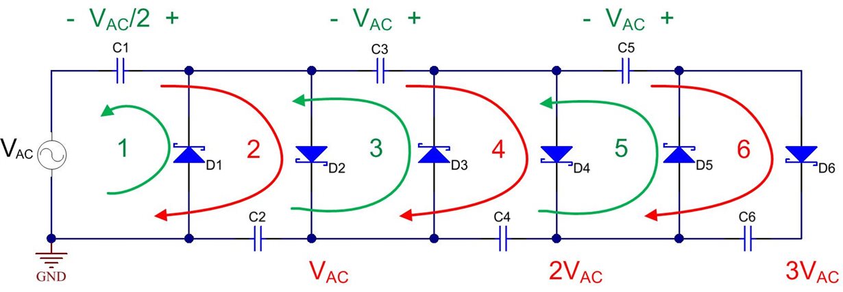
Figure 1 is a schematic illustrating the operation of a three-stage voltage multiplier. The first “doubler” stage comprises C1/D1/C2/D2. The input voltage, VAC, is an alternating square or sinusoidal waveform with a peak-to-peak amplitude equal to VAC. When VAC swings negative to -VAC/2, capacitor C1 charges as diode D1 conducts (the green arrow around the number 1). Let’s ignore the diode forward drops for now. During VAC’s positive half cycle, equal to +VAC /2, the charge stored in C1 transfers to C2 through D2 (the red arrow around the number 2). C2 charges to VAC (VAC/2 from the input voltage plus VAC/2 from the voltage across C1). This doubles the voltage from VAC/2 to VAC.
The second doubler stage comprises C3/D3/C4/D4. During the negative input cycle, C3 charges to VAC (the green arrow around the number 3). This is easy to see because when D1 and D3 conduct, the voltage across C3 is equal to C2. Similarly, on the positive input cycle, C4 charges through D4 (the red arrow around the number 4) to 2*VAC (with respect to ground), since C2 has already charged to a potential of VAC.
The third stage comprises C5/D5/C6/D6 and works identically to the second stage. Capacitor C5 charges to VAC and transfers that voltage to C6, which adds to the previous stages. Each successive stage ideally adds VAC, making it simple to increase the output voltage further.
Figure 1: A voltage multiplier uses an Alternating Current (AC) voltage with diodes and capacitors in a cascade
It becomes clear from the circuit’s operation the voltages at the nodes between the upper set of capacitors switch with the input voltage. The voltages at these nodes all shift between two voltage levels, with the delta equal to VAC (ignoring diode drops). The upper capacitors act as charge pumps, transferring energy into the lower capacitors. The output voltage appears across the lower-series stack of capacitors, with each charged to VAC and holding a constant output voltage. While this is accurate for light loading, the output voltage may begin to sag as the load current is increased since only a fixed amount of energy is transferred in each switching cycle. To improve voltage regulation when the load current is increased, try using larger capacitance values. This is why light loading on the output works best.
The diode forward voltage drops subtract voltage from each stage. The output voltage at the first doubler stage is equal to its peak-to-peak input voltage minus two diode voltage drops, or VC2 = VAC– 2VD. The second stage starts with this voltage, doubles it, and loses two more diode voltage drops for VC4 = 2VAC– 4VD. The output voltage of the third stage is equal to VC6 = 3VAC– 6VD. So, it’s best to start with a VAC that is much larger than two diode voltage drops.
The application report, “TLC555-Q1 Used as a Positive and Negative Charge Pump,” includes an example design which uses a multiplier for both positive and negative output voltages.
Voltage multipliers provide a simple method to create a high-voltage output from nearly any switching voltage. You can easily add additional stages to obtain higher output voltages. Diode forward voltage drops and small capacitance values reduce the output voltage as the load current increases. However, knowing this limitation, a voltage multiplier can boost the output voltage without the need for a transformer or even an inductor. For more information on this topic, see the EETimes Power Tips post, “Increase Output Voltage with a Voltage Multiplier”.
Additional resources
- Check out TI’s Power Tips blog series on Power House.
- Explore more power-supply topics.
- Find a Power Tips video to help with your next design challenge.


