As an applications engineer, I often get inquiries about voltage and current flows in switching regulators. And I often realize that the basic theory I learned in college doesn’t always tell the whole story. A recent case with the asynchronous boost converter in the TPS65150 LCD bias device is a good example of what I mean.
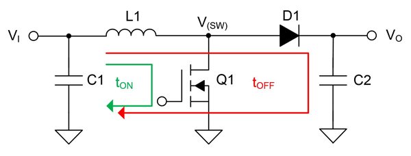
Let’s start with the basic theory of how the switching node of a boost converter should look. Figure 1 shows the basic structure of an asynchronous boost converter.
Figure 1: Simplified boost converter block diagram
When transistor Q1 turns on, the switch node pulls to ground and inductor L1 charges. The voltage on the switch node is approximately equal to 0V during the on time. During the off time, Q1 turns off, L1 discharges to the output, and the voltage on the switch node equals the output voltage (VO) plus the forward voltage (VF) across diode D1.
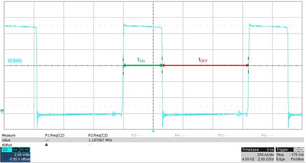
Figure 2 shows the switch-node waveform under typical operating conditions. As expected, the voltage on the switch node is rectangular and alternates between ground and VO + VF.
Figure 2: Switch-node waveform
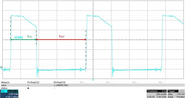
But under low-output current conditions, the switch-node waveform shape changes and looks like Figure 3. At the start of the off time the switch-node voltage is VO + VF (as before), but then it ramps down linearly. What’s causing this behavior and what’s the difference to the basic theory?
Figure 3: Switch-node waveform at low-output currents
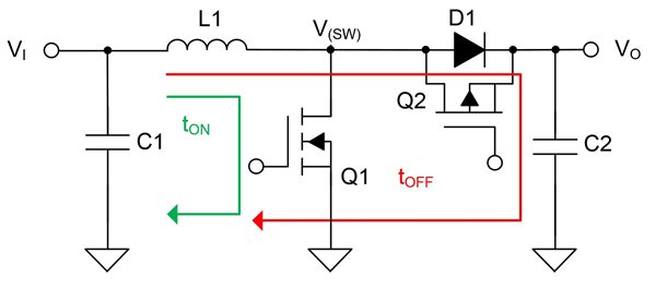
The internal block diagram shown in Figure 4 reveals the reason for the sloping waveform: an additional PMOS transistor (Q2) connected across the diode rectifier. This transistor is a synchronous rectifier that lets the converter operate in continuous conduction mode (CCM) under all operating conditions. It is on when the inductor current is negative and off at all other times. Because it is not the main rectifier, the Rds(on) of Q2 can be relatively high (a few ohms) without decreasing efficiency much, but the high Rds(on) causes a voltage drop on the switch node when the negative inductor current flows through it. And because the inductor current is linearly increasing, the voltage drop also increases, causing the slope shown in Figure 3.
Figure 4: Internal block diagram showing synchronous rectifier
Figure 5 shows the inductor current as well as the switch-node voltage and confirms that the ramp on the switch-node voltage starts when the inductor current goes negative, and increases as the inductor current increases.
Figure 5: Switch-node voltage and inductor-current waveforms
Be aware that the ramp starts for all output currents below the critical conduction point. You can calculate the critical conduction current with Equation 1:

where D is the duty cycle (boost:  ), L is the inductance and is the switching frequency.
If you want get a deeper understanding of voltage and current flows in switching regulators, download the tool, “Power Stage Designer of Most Commonly Used Switch-Mode Power Supplies.
If you have experienced similar waveforms in your power-supply design of power supplies that you cannot explain – but would like to know the reason for, – just add a comment below.
Additional resources:


