Field programmable gate arrays (FPGAs) are increasingly complex system on chips (SoCs) that include not just programmable logic gates and random access memory (RAM) but also analog-to-digital converters (ADCs); digital-to-analog converters (DACs); and programmable analog features and signal-conditioning circuits that enable high-performance digital computations in servers, network-attached storage (NAS), enterprise switches, oscilloscopes, network analyzers, test equipment and software-defined radios.
Altera’s Arria 10 SoC is such an FPGA. One of the Arria 10’s power-reduction techniques is smart voltage ID (SmartVID), which offers a large number of very small-voltage reduction steps that are programmable into the FPGA’s nonvolatile registers in order to reduce the power dissipation of the chip.
The FPGA is smart enough to monitor its own temperature and tell the external Vcore voltage regulator what Vcore value to output to the FPGA in order to minimize its power consumption and increase efficiency. Because the registers use nonvolatile memory (NVM), the new programmed Vcore value becomes the default value after recycling the FPGA power.
Arria 10 SmartVID FPGAs power up at a nominal Vcore voltage of 0.9V; after that, the Vcore value is adjustable down to 0.83V in discrete, small steps.
One of the SmartVID communication interface options between the Arria 10 FPGA and the external Vcore voltage regulator is the PMBus digital serial interface at a 400kHz clock speed. In a PMBus system, the Arria 10 FPGA acts as a PMBus master or a slave – whatever you prefer.
If the Arria 10 is the PMBus master, it will communicate via PMBus to the Vcore voltage regulator (acting as the PMBus slave) the new Vcore value in a range between 0.83V and 0.9V using the standard PMBus command “VOUT_COMMAND” – 21h code. The PMBus master uses the VOUT_COMMAND instruction in the data format retrieved from VOUT_MODE to write voltage ID values to the regulator. The PMBus Vcore regulator will then set its output voltage to the new commanded value as dictated by the FPGA. The voltage ID voltage can change by no more than 10mV per step.
The regulator(s) must meet the static, ripple and dynamic power tolerances listed in the “Arria 10 GX, GT, and SX Device Family Pin Connection Guidelines” during all phases of power delivery after the boot voltage is reached.
To implement SmartVID with PMBus, you must enable PMBus in the FPGA with Quartus Prime software version 15.1. Only the Arria 10 VCC and VCCP rails can use SmartVID; there is an option to combine VCC/VCCP with VCCERAM rail, but then SmartVID implementation is not possible.
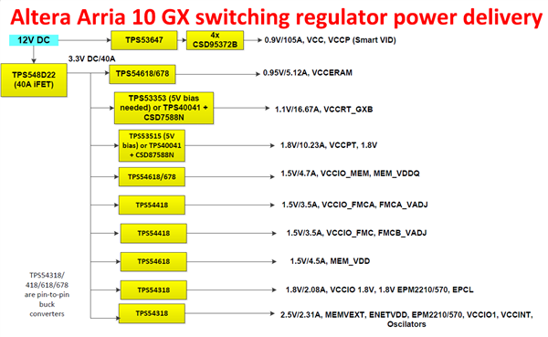
The power tree in Figure 1 corresponds to the Arria 10 GX FPGA, which is the highest-performance Arria 10 member in the SoC family, and shows TI SmartVID solutions for the Arria 10 FPGA core rail through PMBus.

Figure 1 – Altera Arria 10 GX power solution with SmartVID PMBus implementation for VCC/VCCP
The TPS53647 is a PMBus four-phase driverless pulse-width modulation (PWM) controller, with extensive pinstrapping and PMBus programming, configuration, control and monitoring of input/output voltage, current, temperature and power. The TPS53647 is paired with TI’s CSD95372B power stages, which include high-performance NexFET™ gate drivers and high- and low-side NexFET power MOSFETs stacked on top of each other in a PowerStack™ packaging configuration for high efficiency, optimal thermal performance, easy heat sinking and high power density.
So if you are designing with Altera’s Arria 10 FPGAs and looking to implement SmartVID via PMBus, consider TI’s PMBus DC/DC solutions for the VCC and VCCP rails.
Additional resources
- Download a TI Design featuring the TPS53647 and CSD95372B in a PMBus multiphase direct current (DC/DC) converter:
- PMBus Power System for Enterprise Ethernet Switches Reference Design.
- High Efficiency, Power Density 1V/120A/30A/30A (4+1+1) with PMBus Reference Design for ASIC Processors.
- See all of TI’s PMBus power-device portfolio on the Digital Power Control Solutions portal.