It was a cold and snowy day in Toronto.
We were brainstorming in the basement of the local university’s advanced power electronics research lab. Ironically, the conversation was focused on heat – not actually generating it for warmth, but how to reduce it in our power converters. We had pushed MOSFETs and IGBTs to their respective limits, yet none of us were satisfied. Throughout the process, we had accumulated a stack of devices that had failed in our high-stress environment.
On that snowy day, we chose to focus on finding new ways and topologies to get to higher levels of efficiency and density, and of course ways to improve robustness. One of the senior researchers helped summarize our challenge: “We can do all of these ideas. But first, give me the perfect power switch.” The statement was mixed with frustration and hope.
Years later the perfect power switch arrived. In 2018, we released to production our family of 600-V gallium nitride (GaN) FETs with an integrated driver and protection, including the LMG3410R070, LMG3411R070 and LMG3410R050. Each device is capable of megahertz switching and delivering multikilowatt power levels – enabling smaller yet more efficient designs not previously possible.
Before release, TI invested heavily in device robustness for use in every power application to give designers the confidence they need to use GaN, accumulating 20 million hours of device reliability testing in the process.

The “perfect power switch” has arrived
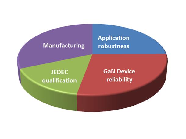
TI has always been on the forefront in advocating for the development and implementation of a comprehensive methodology to ensure the reliable operation and lifetime of GaN devices under the harshest operating conditions. To achieve this, we extended the traditional silicon methodology for GaN and its intrinsic characteristics. Additionally, stress testing needed to include the hard-switching conditions common in switch-mode power supplies, which traditional silicon qualification does not address. TI focused its testing in four categories:
- Device reliability: Pertains to how the device is engineered; establishes the intrinsic lifetime of the device.
- Application robustness: incorporates mission-profile conditions under acceleration to emulate realistic use conditions.
- Manufacturing: focuses on production flow optimization and yield improvement.
- Joint Electron Device Engineering Council (JEDEC) qualification: the quality of the device and its ability to survive accelerated test conditions to predict low defective and failure rates.
 20 million device reliability hours and counting
Additionally, the power electronics industry reached an exciting milestone in 2017. JEDEC announced the formation of JC-70.1 to standardize reliability and qualification procedures, data-sheet elements and parameters, and test and characterization methods for GaN. As a founding and active member of JC-70.1, we at TI are committed to helping the industry further apply the benefits of our methodology, expertise and know-how, building on our 20 million hours of device reliability testing.
The perfect power switch is no longer a fantasy in a cold basement. It’s a reality, and enabling designers to do what they do best: push the envelope to power densities and efficiencies never seen before.
Additional resources
- Read the blog post, “Half the space, double the power: How gallium nitride is revolutionizing robotics, renewable energy, telecom and more.”
- Download these application notes: