In the previous installments of this series, I focused on specification, transfer ratios and basic power ratings, and buck, boost and buck-boost topologies. In this installment, I’ll introduce the single-ended primary inductance converter (SEPIC) and Zeta converter. Both topologies can be a cost-effective alternative to a buck-boost converter in the power range up to 25W.
SEPICs
The SEPIC topology can step up and step down its input voltage. The energy transfers from the input to the output when switch Q1 is not conducting. Figure 1 shows the schematic of a nonsynchronous SEPIC.

Figure 1: Schematic of a nonsynchronous SEPIC
Equation 1 calculates the duty cycle in continuous conduction mode (CCM) as:

Equation 2 calculates the maximum metal-oxide semiconductor field-effect transistor (MOSFET) stress as:

Equation 3 gives the maximum diode stress as:

where Vin is the input voltage, Vout is the output voltage, Vf is the diode forward voltage and VC1,ripple is the voltage ripple across the coupling capacitor.
The inductor-capacitor (LC) filter L1/Ci is pointing to the input of the SEPIC. This leads to a smaller ripple at the input due to the continuous current flow. At the output, the ripple is bigger because there’s a pulsed output current.
A nonsynchronous SEPIC costs less than a buck-boost topology because you need only one gate driver (compared to two for a two-switch buck-boost converter) and only two semiconductor components (instead of four). Another advantage of a SEPIC over a buck-boost topology is the better electromagnetic interference (EMI) behavior when both converters are operating in buck mode as a result of the SEPIC’s continuous input current.
You can easily build a SEPIC by using a boost controller because MOSFET Q1 needs to be driven on the low side.
The right half-plane zero (RHPZ) is the limiting factor for a SEPIC’s achievable regulation bandwidth. The maximum bandwidth is roughly one-fifth the RHPZ frequency. Equation 4 calculates an estimation of the single RHPZ frequency of the SEPIC’s transfer function:

Solving Equation 5 for s will have either one or two more RHPZ(s) as a result:

where Vout is the output voltage, D is the duty cycle, Iout is the output current, L1 is the inductance of inductor L1, L2 is the inductance of inductor L2, C1 is the capacitance of coupling capacitor C1 and s is the complex frequency variable.
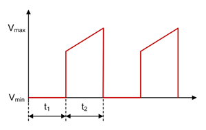
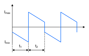
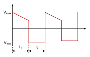
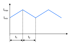
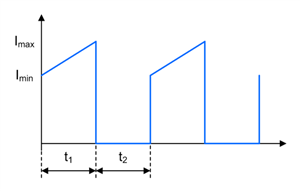
Figures 2 through 11 show voltage and current waveforms in CCM for FET Q1, inductor L1, coupling capacitor C1, diode D1 and inductor L2 in a nonsynchronous SEPIC.
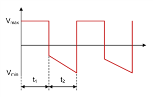
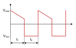
Figure 2: SEPIC FET Q1 voltage waveform in CCM |
Figure 3: SEPIC FET Q1 current waveform in CCM |
Figure 4: SEPIC inductor L1 voltage waveform in CCM |
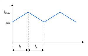
Figure 5: SEPIC inductor L1 current waveform in CCM |
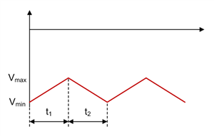
Figure 6: SEPIC coupling capacitor C1 voltage waveform in CCM |
Figure 7: SEPIC coupling capacitor C1 current waveform in CCM |
Figure 8: SEPIC diode D1 voltage waveform in CCM |
Figure 9: SEPIC diode D1 current waveform in CCM |
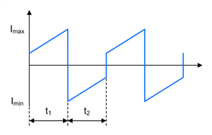
Figure 10: SEPIC inductor L2 voltage waveform in CCM |
Figure 11: SEPIC inductor L2 current waveform in CCM |


Zeta converters
The Zeta topology can step up and step down its input voltage. The energy transfers from the input to the output when switch Q1 is conducting. Figure 12 shows the schematic of a nonsynchronous Zeta converter.
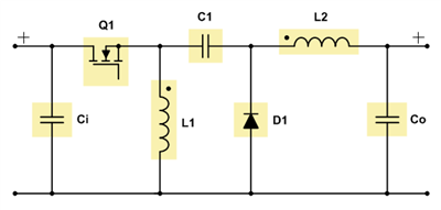
Figure 12: Schematic of a nonsynchronous Zeta converter
Equation 6 calculates the duty cycle in CCM as:

Equation 7 calculates the maximum MOSFET stress as:

Equation 8 gives the maximum diode stress as:

where Vin is the input voltage, Vout is the output voltage, Vf is the diode forward voltage and VC1,ripple is the voltage ripple across the coupling capacitor.
The LC filter L2/Co in a Zeta converter is pointing to the output. As a result, the output ripple is smaller compared to the input ripple, because the output current is continuous and the input current is pulsed. I recommend using the Zeta topology for very sensitive loads, where a SEPIC or buck-boost converter would not fit due to their higher output ripple. The Zeta topology has the same advantage regarding cost and component count over the buck-boost converter as the SEPIC.
You can build a Zeta converter by using a buck controller or converter; you will need a P-channel MOSFET or high-side MOSFET driver.
The Zeta converter does not have a RHPZ, as the controller can immediately react to changes at the output. Therefore, you can achieve higher bandwidths with a Zeta converter than with a SEPIC or buck-boost converter while using less output capacitance.
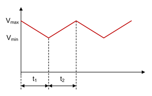
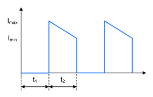
Figures 13 through 22 show voltage and current waveforms in CCM for FET Q1, inductor L1, coupling capacitor C1, diode D1 and inductor L2 in a nonsynchronous Zeta converter.
Figure 13: Zeta FET Q1 voltage waveform in CCM |
Figure 14: Zeta FET Q1 current waveform in CCM |
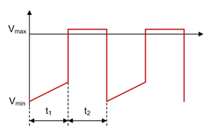
Figure 15: Zeta inductor L1 voltage waveform in CCM |
Figure 16: Zeta inductor L1 current waveform in CCM |
Figure 17: Zeta coupling capacitor C1 voltage waveform in CCM |
Figure 18: Zeta coupling capacitor C1 current waveform in CCM |
Figure 19: Zeta diode D1 voltage waveform in CCM |
Figure 20: Zeta diode D1 current waveform in CCM |
Figure 21: Zeta inductor L2 voltage waveform in CCM |
Figure 22: Zeta inductor L2 current waveform in CCM |


For both topologies, using coupled inductors instead of two separate inductors has two advantages. The first advantage is that only half the inductance is required for a similar current ripple (compared to a two-inductor solution) because of ripple cancellation by coupling the windings. The second advantage is that you can get rid of the resonance in the transfer function caused by the two inductors and the coupling capacitor. You usually need to dampen this resonance with a resistor-capacitor (RC) network in parallel with coupling capacitor C1.
One drawback to using coupled inductors is that you must use the same inductance value for both inductors. Another limitation is typically their current rating. For applications with high output currents, you might need to use single inductors instead.
You can configure both topologies as a converter with synchronous rectification. But if you do, you need to AC-couple the high-side gate-drive signal, because many controllers require that you connect them to the switch node. Both topologies have two switch nodes each, so take care to avoid negative voltage-rating violations on the switch pin. Two examples with a synchronous SEPIC and a synchronous Zeta converter are the 12V@5A Synchronous SEPIC Converter Reference Design and the 40W Synchronous Zeta Converter with Two Inductors Reference Design, respectively.
Additional resources
- Watch these TI training videos:
- Read these Analog Applications Journal articles:
- Design your power stage with Power Stage Designer.
- Download the “Power Topologies Handbook” and “Power Topologies Quick Reference Guide.”


