Many applications today require an input-voltage rating beyond the VIN max ratings of many DC-to-DC controllers. Traditional options include using expensive front-end protection or implementing a low-side gate-drive device, which means employing an isolated topology such as a flyback converter. Isolated topologies often require custom magnetics and increase design complexity and cost compared to a nonisolated approach.
But another alternative exists that enables you to resolve the issue by using a simple buck controller with a VIN max less than the system input voltage. How is this possible?
Buck controllers typically derive a bias supply referenced from ground potential (0V) (Figure 1a). The bias supply is derived from the input; therefore, the device needs to withstand the full VIN potential. However, P-channel buck controllers have the gate-drive supply referenced to VIN (Figure 1b), because the gate-drive voltage required to turn on the P-channel metal-oxide semiconductor field-effect transistor (MOSFET) is at VGS below VIN. To turn off the P-channel MOSFET, the gate voltage simply goes to VIN (0V VGS) (Figure 2).

Figure 1: VCC bias generation for N-channel (a); and P-channel controllers (b)

Figure 2: Gate drive for a P-Channel controller
The fact that the nonsynchronous P-channel controller derives its bias supply to drive the P-channel gate in this way is a huge benefit and makes it possible to supply a virtual ground that floats above a 0V potential. For an N-channel high side MOSFET the voltage is derived from a supply that is referenced to ground. This is charge pumped using a boot capacitor and diode to supply a gate voltage higher than its source potential of VIN. With a P-channel high side MOSFET, things are a lot simpler. To turn on the P-channel MOSFET, the gate potential needs to be lower than its source potential of VIN. Therefore the supply is referenced to VIN only and not VIN and ground as described above.
Floating ground
How can you create a floating ground for the controller? It’s quite simple: by using an emitter follower. Figure 3 shows a basic implementation of such a scheme. The emitter of the P-channel N-channel P-channel (PNP) will sit at a potential that is Vbe (~0.7V) below the Zener diode voltage potential (Vz). In essence, you’re floating the controller to VIN and regulating the reference of the controller to limit the voltage between VIN and the device ground.

Figure 3: Creating a virtual ground using a simple emitter follower scheme
Output-voltage translation
There is one challenge to overcome. Because the controller is sitting on a virtual ground (Vz-Vbe) and generating a step-down output voltage that is referenced to ground (0V) potential, how are you going to translate the output-voltage signal to a feedback voltage (typically between 0.8V and 1.25V) sitting above a virtual ground? Figure 4 illustrates the challenge.

Figure 4: Schematic showing the difference in voltage potential between VOUT (referenced to 0V ground) and the feedback voltage of a controller (referenced to virtual ground)
To close the loop, you can implement Figure 5 by using a couple of matched-pair transistors. One pair sends the feedback signal to VIN; the other matched pair generates a current from VIN to a potential above the virtual ground.

Figure 5: High-level schematic of a nonsynchronous controller and feedback implementation using matched-pair transistors
Putting it all together
The LM5085 is ideal for the application I’ve described because it is a P-channel nonsynchronous controller whose VCC bias supply is referenced to VIN. The LM5085 can withstand input voltages up to 75VIN in traditional applications. For applications with input transient voltages much higher than 75V, consider the solution presented here, specified for an output of 12V.
Starting from the controller feedback voltage of 1.25V and using a current to generate the feedback (Ifb) set to 1mA, calculate the Rfb value using Equation 1:

where Rfb = 1.25k.
Rfb1 sets the reference current for the current mirrors. Once again, with 1mA as the reference current and using Equation 2, calculate Rfb1 to set the output voltage:

where VOUT = 12V, Rfb1 = 11.3k and Vbe is ~0.7V.
With 1mA flowing into Rfb2 and the emitter current being approximately equal to the collect current (Ie~Ic), this sets the reference current Iref2. The loop is closed and the voltage will regulate to the set voltage described.
Output voltage regulation
One possible application this idea is suitable for is when voltage transients are significantly higher than the absolute maximum of the LM5085. The LM5085 is a constant on-time (COT) controller; as such, its on-time (Ton) is inversely proportional to VIN. However, when clamping the VIN to the LM5085, Ton will no longer adjust with increasing VIN (to the power stage) because the device will have a fixed voltage set by the Zener diode while the Vin to the power stage is increasing. This will cause the frequency to drop as the input voltage to the power stage increases beyond the clamping voltage to the LM5085; the regulation voltage may begin to increase slightly as a result. Therefore, take care to size the ripple-injection voltage using a Type 1 ripple-injection scheme, thus ensuring that the ripple is set within acceptable limits to maintain stability and minimize error on the output from increasing ripple.
Example schematic
Figure 6 shows an example schematic of a 48V supply with an absolute maximum VIN rating of 150V. The example board can deliver 12VOUT at 3A.
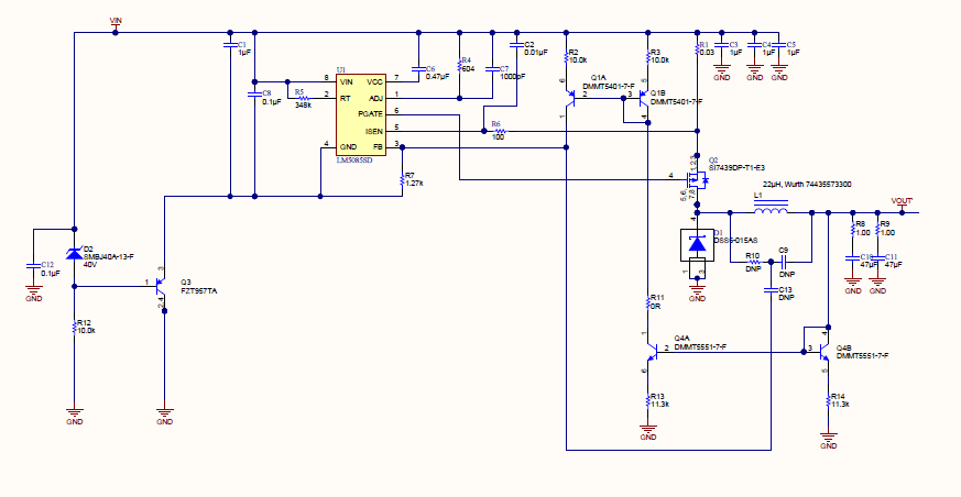
Figure 6: A 24V to 150VIN (max)/12VOUT at 3A design using the LM5085
Figure 7 shows an efficiency plot taken from a prototype board, with efficiency (%) vs. load current (A).
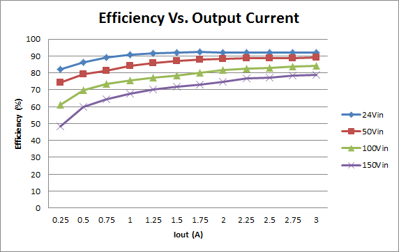
Figure 7: Efficiency (%) vs. load current (A) at various input voltages
Figure 8shows the switch-node voltage and inductor ripple current at 150VIN.

Figure 8: Channel 1 switch-node voltage, channel 4 inductor ripple current
Conclusion
You can use a P-channel nonsynchronous buck controller in applications where the input voltage of the system exceeds the maximum input-voltage rating of the device. This application has the benefit of using a lower-cost controller with minimal component count. For design guidance on the power stage of the buck converter, please see the application information in the LM5085 data sheet.