In the second installment of this blog series, I discussed how to choose the best-fitting topology from the parameters of your power-supply specification. In this third installment, I’ll describe different in-depth aspects for buck, boost and buck-boost topologies.
Buck converters
Figure 1 shows the schematic of a nonsynchronous buck converter. A buck converter steps down its input voltage to a lower output voltage. The energy transfers to the output when switch Q1 is conducting.

Figure 1: Schematic of a nonsynchronous buck converter
Equation 1 calculates the duty cycle as:

Equation 2 calculates the maximum metal-oxide semiconductor field-effect transistor (MOSFET) stress as:

Equation 3 gives the maximum diode stress as:

where is the input voltage, is the output voltage and is the diode forward voltage.
The bigger the difference between the input voltage and output voltage, the greater the buck converter’s efficiency compared to a linear regulator or low-dropout regulator (LDO).
While a buck converter has a pulsed current at the input, the output current is continuous due to the inductor-capacitor (LC) filter located at the converter’s output. As a result, the voltage ripple reflected to the input will be larger compared to the ripple at the output.
For buck converters with a small duty cycle and output currents greater than 3A, I recommend using a synchronous rectifier. If your power supply requires output currents greater than 30A, I recommend a multiphase or interleaved power stage, as this minimizes the stress for components, spreads the generated heat among multiple power stages and reduces the reflected ripple at the converter’s input.
Duty-cycle limitations can occur when using an N-FET, because the bootstrap capacitor needs to be recharged every switching cycle. In this case, the maximum duty cycle is in the range of 95-99%.
Buck converters have in general good dynamic behavior because they represent a forward topology. The achievable bandwidth depends on the quality of the error amplifier and the chosen switching frequency.
Figures 2 through 7 show voltage and current waveforms in continuous conduction mode (CCM) for the FET, diode and inductor in a nonsynchronous buck converter.

Boost converters
A boost converter steps up its input voltage to a larger output voltage. The energy transfers to the output when switch Q1 is not conducting. Figure 8 is a schematic of a nonsynchronous boost converter.

Figure 8: Schematic of a nonsynchronous boost converter
Equation 4 calculates the duty cycle as:

Equation 5 calculates the maximum MOSFET stress as:

Equation 6 gives the maximum diode stress as:

where is the input voltage, is the output voltage and is the diode forward voltage.
With a boost converter, you can see a pulsed output current, as the LC filter is located at the input. Thus, the input current is continuous and the output voltage ripple is larger than the input voltage ripple.
When designing a boost converter, it is important to know that there is a permanent connection from the input to the output, even when the converter is not switching. You have to take precautions in case of a possible short event at the output.
For output currents greater than 4A, you should replace the diode with a synchronous rectifier. In case your power-supply needs to provide output currents greater than 10A, I highly recommend a multiphase or interleaved power-stage approach.
When operating in CCM, the dynamic behavior of a boost converter is limited due to the right half-plane zero (RHPZ) of its transfer function. Because the RHPZ cannot be compensated, the achievable bandwidth will usually be less than one-fifth to one-tenth the RHPZ frequency. See Equation 7:

where is the output voltage, is the duty cycle, is the output current and is the inductance of the boost converter.
Figures 9 through 14 show the voltage and current waveforms in CCM for the FET, diode and inductor in a nonsynchronous boost converter.

Buck-boost converters
A buck-boost converter is a combination of a buck and a boost power stage, which share the same inductor. See Figure 15.
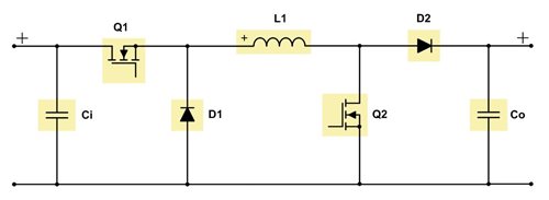
Figure 15: Schematic of a two-switch buck-boost converter
The buck-boost topology is useful because the input voltage can be smaller, greater or equal to the output voltage, while the output power needed is bigger than 50W.
For an output power smaller than 50W, a single-ended primary inductance converter (SEPIC) is a more cost-effective choice because it uses less components.
A buck-boost converter operates in buck mode when the input voltage is greater than the output voltage, and in boost mode for input voltages smaller than the output voltage. When the converter is operating in the transfer region, which is when the input voltage is in the range of the output voltage, there are two concepts for handling these conditions: either both the buck and boost stage are active at the same time, or the switching cycles alternate between the buck and boost stages, each usually running at half the regular switching frequency. The second concept can cause subharmonic noise at the output and the output-voltage precision can be a little bit less accurate compared to regular buck or boost operation, but the converter will be much more efficient compared to the first concept.
The buck-boost topology has pulsed currents at the input and the output, as there is no LC filter pointing in either direction.
You can use the buck and boost power-stage calculations, respectively, for a buck-boost converter.
Buck-boost converters with two switches are suitable for a power range between 50W and 100W (such as the LM5118), with synchronous rectification up to 400W possible (as with the LM5175). I advise using synchronous rectifiers with the same current limits as for the uncombined buck and boost power stages.
You need to design the compensation network of a buck-boost converter for the boost stage, because the RHPZ will be the limiting factor of the regulator’s bandwidth.
In my next post, I will discuss the features and drawbacks of the SEPIC and Zeta converter.
Additional resources
- Watch these TI training videos: